isolated current voltage transducers

Create successful ePaper yourself
Turn your PDF publications into a flip-book with our unique Google optimized e-Paper software.
Miscellaneous<br />
8 Miscellaneous<br />
Here are additional concerns when using the types of<br />
measurement devices described in this document.<br />
8.1 Power supply polarity inversion<br />
A LEM transducer may be damaged by an inversion of the<br />
power supply <strong>voltage</strong> or connection of supply <strong>voltage</strong>s to the<br />
output or common pins. If this is a concern, LEM advises the<br />
user to insert a diode on each power supply line, both<br />
positive and negative, or to look for a specific LEM transducer<br />
that incorporates these protection diodes.<br />
8.2 Capacitive dv/dt noise<br />
Any electrical component with galvanic isolation has<br />
capacitive coupling between the <strong>isolated</strong> potentials.<br />
Applications with fast switching speeds, and consequently<br />
fast <strong>voltage</strong> changes (dv/dt), across this capacitance<br />
experience some coupling of the primary transient to the<br />
secondary side creating undesirable interferences.<br />
For example, a <strong>voltage</strong> change of 10 kV/µs in combination<br />
with a 10 pF coupling capacitance generates a parasitic<br />
<strong>current</strong> of i = C • dv/dt = 100mA. This represents an error of<br />
two times the nominal output <strong>current</strong> for a transducer with a<br />
50 mA nominal output.<br />
This issue typically occurs with power converters where a<br />
power component, such as a MOSFET (Metal Oxide<br />
Semiconductor Field Effect Transistor) or IGBT (Insulated<br />
Gate Bipolar Transistor), switch the <strong>voltage</strong> at frequencies in<br />
the 10 kHz to 1 MHz range, generating dv/dt values in the<br />
5 to 50 kV/µs range.<br />
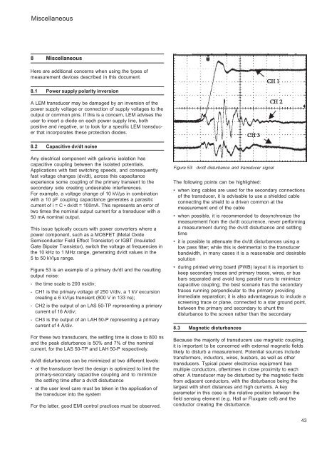
Figure 53 is an example of a primary dv/dt and the resulting<br />
output noise:<br />
- the time scale is 200 ns/div;<br />
- CH1 is the primary <strong>voltage</strong> of 250 V/div, a 1 kV excursion<br />
creating a 6 kV/µs transient (800 V in 133 ns);<br />
- CH2 is the output of an LAS 50-TP representing a primary<br />
<strong>current</strong> of 16 A/div;<br />
- CH3 is the output of an LAH 50-P representing a primary<br />
<strong>current</strong> of 4 A/div.<br />
For these two <strong>transducers</strong>, the settling time is close to 800 ns<br />
and the peak disturbance is 50% and 7% of the nominal<br />
<strong>current</strong>, for the LAS 50-TP and LAH 50-P respectively.<br />
dv/dt disturbances can be minimized at two different levels:<br />
• at the transducer level the design is optimized to limit the<br />
primary-secondary capacitive coupling and to minimize<br />
the settling time after a dv/dt disturbance<br />
• at the user level care must be taken in the application of<br />
the transducer into the system<br />
For the latter, good EMI control practices must be observed.<br />
Figure 53: dv/dt disturbance and transducer signal<br />
The following points can be highlighted:<br />
• when long cables are used for the secondary connections<br />
of the transducer, it is advisable to use a shielded cable<br />
connecting the shield to a driven common at the<br />
measurement end of the cable<br />
• when possible, it is recommended to desynchronize the<br />
measurement from the dv/dt occurrence, never performing<br />
a measurement during the dv/dt disturbance and settling<br />
time<br />
• it is possible to attenuate the dv/dt disturbances using a<br />
low pass filter; while this is detrimental to the transducer<br />
bandwidth, in many cases it is a reasonable and desirable<br />
solution<br />
• during printed wiring board (PWB) layout it is important to<br />
keep secondary traces and primary traces, wires, or bus<br />
bars separated and avoid long parallel runs to minimize<br />
capacitive coupling; the best scenario has the secondary<br />
traces running perpendicular to the primary providing<br />
immediate separation; it is also advantageous to include a<br />
screening trace or plane, connected to a star ground point,<br />
between the primary and secondary to shunt the<br />
disturbance to the screen rather than the secondary<br />
8.3 Magnetic disturbances<br />
Because the majority of <strong>transducers</strong> use magnetic coupling,<br />
it is important to be concerned with external magnetic fields<br />
likely to disturb a measurement. Potential sources include<br />
transformers, inductors, wires, busbars, as well as other<br />
<strong>transducers</strong>. Typical power electronics equipment has<br />
multiple conductors, oftentimes in close proximity to each<br />
other. A transducer may be disturbed by the magnetic fields<br />
from adjacent conductors, with the disturbance being the<br />
largest with short distances and high <strong>current</strong>s. A key<br />
parameter in this case is the relative position between the<br />
field sensing element (e.g. Hall or Fluxgate cell) and the<br />
conductor creating the disturbance.<br />
43