

SIM0216

Create successful ePaper yourself
Turn your PDF publications into a flip-book with our unique Google optimized e-Paper software.
VOLUME 18<br />
MAY 2016<br />
69721<br />
2<br />
Official Partner of the EMS<br />
High-Throughput Confocal Imaging<br />
Integrated Raman-FIB-SEM<br />
Multi-Tip SPM<br />
Single Molecular Spectroscopy
Editorial<br />
Image: Alexander Tselev and Andrei Kolmakov, ORNL<br />
Nano-Imaging with Microwaves<br />
Martin Friedrich,<br />
Editor-in-Chief<br />
Thomas Matzelle,<br />
Scientific Editor<br />
Nanoscale imaging in liquids is quite<br />
challenging: High-resolution imaging<br />
techniques that use energetic electron<br />
beams and X-rays often have a destructive<br />
effect on the sample.<br />
Surface researchers at the Oak Ridge<br />
National Laboratory, Tennessee, and the<br />
National Institute of Standards and Technology,<br />
Gaithersburg, Maryland, have recently<br />
demonstrated a non-destructive<br />
method for imaging objects and processes<br />
on the nanoscale in a liquid environment.<br />
Alexander Tselev, Andrei Kolmakov<br />
and their colleagues recommend<br />
an “environmental chamber” to encapsulate<br />
the sample in a liquid. In detail, the<br />
chamber has a window made of an ultra-thin<br />
membrane, not thicker than 50<br />
nm. The amazing part of the methodological<br />
set-up is the tiny tip of a scanning<br />
probe microscope that moves across the<br />
membrane injecting microwaves into the<br />
chamber. A high-resolution map of the<br />
sample is revealed when recording the<br />
transmitted versus the impeded microwave<br />
signal. This new methodological approach<br />
of combining scanning probe microscopy<br />
with microwaves and ultrathin<br />
membranes is called scanning microwave<br />
impedance microscopy (sMIM).<br />
Neutron scattering and X-ray diffraction<br />
are typical methods of choice<br />
when imaging crystals and other highly<br />
oriented materials. A promising new<br />
method is now to hand for microscopists<br />
when studying less ordered materials,<br />
like living cells and processes such as ongoing<br />
chemical reactions.<br />
A microwave oven heats aqueous liquids,<br />
as we all know. However, the microwaves<br />
injected in this way in sMIM are<br />
millions of times weaker and they oscillate<br />
in opposite directions. Thus, sMIM<br />
only produces negligible heat and potentially<br />
destructive chemical reactions cannot<br />
proceed. “Our imaging is nondestructive<br />
and free from the damage frequently<br />
caused to samples, such as living cells or<br />
electro-chemical processes by imaging<br />
with X-ray or electron beams,” said first<br />
author of the original publication in ACS<br />
Nano, Alexander Tselev. “Its spatial resolution<br />
is better than that achievable with<br />
optical microscopes for similar in-liquid<br />
samples. The paradigm could become instrumental<br />
in gaining important insights<br />
into electro-chemical phenomena, living<br />
objects and other nanoscale systems existing<br />
in fluids.”<br />
The applicability of sMIM has already<br />
been proven on different samples, especially<br />
living cells. The ORNL-NIST team<br />
has demonstrated, that to detect properties<br />
which distinguish healthy cells from<br />
sick ones: “If you have microwaves, you<br />
can go variably in depth and get a lot of<br />
information about the living, biological<br />
cell membrane itself - shape and properties<br />
that depend very much on the<br />
chemical composition and water content,<br />
which in turn depend on whether the cell<br />
is healthy or not,” Tselev said.<br />
Although current experiments have<br />
provided promising results regarding the<br />
applicability of the method for observations<br />
close to the surface, due to the nature<br />
of microwaves, sMIM is feasible for<br />
seeing deeper inside the sample.<br />
In future the researchers will try to<br />
further reduce the thickness of the membrane<br />
and to use probes and image-processing<br />
algorithms to improve the sensitivity<br />
of the system and the spatial<br />
resolution in depth.<br />
The stage is set for exciting and challenging<br />
advances in this field.<br />
References<br />
Dawn Levy: ORNL-NIST team explores nanoscale<br />
objects and processes with microwave microscopy,<br />
www.ornl.gov (2016)<br />
Alexander Tselev et al.: Seeing Through Walls at<br />
the Nanoscale: Microwave Microscopy of Enclosed<br />
Objects and Processes in Liquids, ACS Nano, 10 (3),<br />
pp 3562–3570 (2016)<br />
G.I.T. Imaging & Microscopy 2/2016 • 3
Official Partner of the EMS<br />
Contents<br />
69721<br />
VOLUME 18<br />
MAY 2016<br />
2<br />
Official Partner of the EMS<br />
EDITORIAL 3<br />
NEWSTICKER 6<br />
EVENT CALENDER 8<br />
ANNOUNCEMENT<br />
Bioimaging: from Cells to Molecules / EMBL Events 9<br />
High-Throughput Confocal Imaging<br />
Integrated Raman-FIB-SEM<br />
Multi-Tip SPM<br />
Single Molecular Spectroscopy<br />
European Microscopy Congress 2016 10<br />
SPAOM 2016 11<br />
Webinar: Fluorescence Lifetime Imaging 12<br />
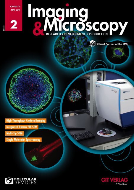
COVER<br />
High-Throughput Confocal<br />
Imaging of 3D Spheroids<br />
Cover images show examples of some of<br />
the many automated imaging applications<br />
that are enabled using the new ImageXpress<br />
Micro Confocal High-Content Imaging<br />
System from Molecular Devices, including<br />
3D-spheroid imaging, tissue imaging, slide<br />
scanning, protein co-localization, fast kinetic<br />
processes such as beating cardiomyocytes,<br />
and whole organism (e.g. zebrafish) imaging.<br />
With the ImageXpress Micro Confocal<br />
you can run 3D cellular assays with confocal<br />
results — at a speed you’d only expect from<br />
widefield screening.<br />
16<br />
READ & WIN<br />
Handbook of Fluorescence Spectroscopy and Imaging 13<br />
From Single Molecules to Ensembles<br />
RMS IN FOCUS<br />
mmc2017 – It’s Your Congress 14<br />
NEWS FROM EMS<br />
EMS Newsletter 53, May 2016 15<br />
COVER STORY<br />
High-Throughput Confocal Imaging of 3D Spheroids 16<br />
Screening Cancer Therapeutics<br />
O. Sirenko<br />
LIGHT MICROSCOPY<br />
PREVIEW: ISSUE 3<br />
coming out August 17, 2016<br />
Diffusion Measurements in C. Elegans Embryos 18<br />
Using Single Plane Illumination Microscopy Combined with Fluorescence<br />
Correlation Spectroscopy<br />
P. Struntz et al.<br />
Single Molecular Spectroscopy 21<br />
Parallel Lifetime and Imaging of Single Molecules<br />
A. Mantsch and A. Cadby<br />
Water Wetting on Sub-Micron Scale<br />
Leaf Surfaces Studied with In Situ Electron<br />
Microscopy<br />
M. Koch<br />
TEM Imaging and TKD Mapping<br />
Interaction of Nanoparticles Incorporated in a<br />
Nickel Matrix<br />
D. Dietrich, T. T. Lampke, A. A. Sadeghi<br />
4 • G.I.T. Imaging & Microscopy 2/2016
Quality Control of Fluorescence Imaging Systems 24<br />
A New Tool for Performance Assessment and Monitoring<br />
A. Royon and N. Converset<br />
Observing the 3rd Dimension 28<br />
A Simple Way to Upgrade Common Microscopes for Sample Rotation<br />
T. Bruns et al.<br />
<br />
<br />
<br />
SCANNING PROBE MICROSCOPY<br />
The Multimeter at the Nanoscale 31<br />
Charge Transport at the Nanoscale Measured by a Multi-Tip<br />
Scanning Probe Microscope<br />
B. Voigtländer<br />
ELECTRON MICROSCOPY<br />
Integrated Raman – FIB – SEM 34<br />
A Correlative Light and Electron Microscopy Study<br />
F. Timmermans et al.<br />
<br />
Spectra of Electrons Emerging from PMMA 38<br />
Monte Carlo Simulation of Electron Energy Distributions<br />
M. Dapor<br />
Stemming Unwanted Interference 40<br />
Resolution Improvement by Incoherent Imaging with ISTEM<br />
F. Krause<br />
<br />
<br />
Electro-Optical Characterization of 3D-LEDs 44<br />
Nondestructive Inspection of 4” Wafers in Bird’s Eye View by an FE-SEM<br />
J. Ledig et al.<br />
PRODUCTS 47<br />
INDEX / IMPRINT<br />
INSIDE BACK COVER<br />
<br />
<br />
Congratulation<br />
The winner of Read & Win issue<br />
1/2016 is Pawel Drozdzal from<br />
Adam Mickiewicz University<br />
Polen.<br />
The next prize draw is on page 50<br />
<br />
G.I.T. Imaging & Microscopy 2/2016 • 5
NEWSTICKER<br />
High-Resolution Microscopy<br />
New Open Source Software<br />
With their special microscopes,<br />
experimental physicists<br />
can already observe single<br />
molecules. However,<br />
unlike conventional light microscopes,<br />
the raw image<br />
data from some ultra-high<br />
© University of Bielefeld<br />
resolution instruments first<br />
have to be processed for an image to appear. For the ultra-high resolution fluorescence<br />
microscopy that is also employed in biophysical research at Bielefeld<br />
University, members of the Biomolecular Photonics Group have developed a<br />
new open source software solution that can process such raw data quickly and<br />
efficiently.<br />
Original publication:<br />
Marcel Müller et al.: Open source image reconstruction of super-resolution<br />
structured illumination microscopy data in ImageJ, Nature Communications<br />
(2016) doi:10.1038/ncomms10980<br />
Laser Technology<br />
Changing the Orbital Angular Momentum of Laser Beams<br />
Researchers from South Africa and Italy<br />
demonstrating a new type of laser that is<br />
able to produce laser beams ‘with a<br />
twist’ as its output. These so-called vector<br />
vortex beams are represented on a<br />
higher-order Poincare sphere. Using geometric<br />
phase inside lasers for the first<br />
time, the work opens the way to novel<br />
lasers for optical communication, laser<br />
© University of the Witwatersrand<br />
machining and medicine.<br />
Original publication:<br />
Darryl Naidoo et al.: Controlled generation of higher-order Poincaré sphere<br />
beams from a laser, Nature Photonics (2016) doi: 10.1038/nphoton.2016.37<br />
More information:<br />
http://bit.ly/IM-22016-b<br />
More information:<br />
: http://bit.ly/IM-22016-a<br />
CLAIRE<br />
Super-Resolution Imaging<br />
Multiplexed Morse Signals from Cells<br />
How many sorts, in how many copies?<br />
The biochemical processes that take<br />
place in cells require specific molecules<br />
to congregate and interact in specific locations.<br />
A novel type of high-resolution<br />
microscopy developed at the Max<br />
Planck Institute of Biochemistry in Martinsried,<br />
Germany and Harvard Univer-<br />
© MPI Biochemistry<br />
sity, USA, already allows researchers to visualize these molecular complexes and<br />
identify their constituents. Now they can also determine the numbers of each molecular<br />
species in these structures. Such quantitative information is valuable for<br />
the understanding of cellular mechanisms and how they are altered in disease<br />
states.<br />
Original publication:<br />
Ralf Jungmann et al.: Quantitative super-resolution imaging with qPAINT,<br />
Nature Methods (2016) doi: 10.1038/nmeth.3804<br />
Non-Invasive Electron Microscopy for Soft Materials<br />
Using the Molecular<br />
Foundry’s imaging capabilities,<br />
scientists developed<br />
a technique, called<br />
“CLAIRE,” that allows<br />
the incredible resolution<br />
of electron microscopy<br />
© Molecular Foundry to be used for non-invasive<br />
imaging of biomolecules and other soft matter. The new technique offers<br />
both clarity and speed. CLAIRE could lead to the understanding of key biological<br />
processes and help accelerate the development of new technologies such as<br />
high-efficiency photovoltaic cells.<br />
Original publications:<br />
Connor G. Bischak et al.: Cathodoluminescence-activated nanoimaging: Noninvasive<br />
near-field optical microscopy in an electron microscope, Nano Letters<br />
(2015) doi: 10.1021/acs.nanolett.5b00716<br />
More information:<br />
http://bit.ly/IM-22016-d<br />
More information:<br />
http://bit.ly/IM-22016-f<br />
MOZART<br />
Imaging Cells and Tissues<br />
under the Skin<br />
Scientists have many tools at their disposal<br />
for looking at preserved tissue<br />
under a microscope in incredible detail,<br />
or peering into the living body at<br />
lower resolution. What they haven’t<br />
had is a way to do both: create a threedimensional<br />
real-time image of individual<br />
cells or even molecules in a living<br />
animal. Now, Stanford scientists<br />
have provided the first glimpse under<br />
the skin of a living animal, showing intricate<br />
real-time details in three dimensions<br />
of the lymph and blood vessels.<br />
The technique, called MOZART<br />
(for MOlecular imaging and characteri-<br />
Zation of tissue noninvasively At cellular<br />
ResoluTion), could one day allow<br />
scientists to detect tumors in the skin,<br />
colon or esophagus, or even to see the<br />
abnormal blood vessels that appear in<br />
the earliest stages of macular degeneration<br />
– a leading cause of blindness.<br />
More information:<br />
http://bit.ly/IM-22016-g<br />
6 • G.I.T. Imaging & Microscopy 2/2016
Newsticker<br />
Electron Microscopy<br />
Real-Time Direct Observation of Atom Movements<br />
Atomic motion in a crystalline<br />
oxide that was used as a cathode<br />
in Lithium-ion batteries was directly<br />
demonstrated by state-ofan-art<br />
transmission electron microscopy,<br />
revealing the transient<br />
pathway of a chemical ordering<br />
reaction. Researchers from Korea<br />
have successfully demonstrated<br />
© KAIST<br />
how the cation ordering occurs in<br />
Li(Mn 1.5 Ni 0.5 )O 4 spinel, which is a promising cathode material for high-voltage<br />
Li-ion batteries.<br />
Original publication:<br />
Hyewon Ryoo et al. : Frenkel-Defect-Mediated Chemical Ordering Transition in a<br />
Li-Mn-Ni Spinel Oxide, Angewandte Chemie, (2015) doi: 10.1002/<br />
ange.201502320<br />
More information:<br />
http://bit.ly/IM-22016-e<br />
Medical Imaging<br />
Breaking Bonds for Probes and Drugs<br />
A chemical procedure developed<br />
by an all-RIKEN research team has<br />
the potential to enhance the usefulness<br />
of positron emission tomography<br />
(PET) for discovering<br />
new drugs and diagnosing diseases.<br />
Compounds known as<br />
© RIKEN<br />
fluoroarenes are suitable starting materials for making fluorine-containing<br />
probes. But to transform them into useful probes requires breaking one of the<br />
strongest bonds in nature the carbon–fluorine bond. This is the key process that<br />
researchers have now achieved. They used a nickel–copper catalyst to break the<br />
carbon–fluorine bond in a way that permits non-radioactive fluorine-19 atoms to<br />
be swapped with radioactive counterparts, fluorine-18 atoms.<br />
Original publication:<br />
Niwa T. et al.: Ni/Cu-catalyzed defluoroborylation of fluoroarenes for diverse<br />
C–F bond functionalizations, Journal of the American Chemical Society (2015)<br />
doi: 10.1021/jacs.5b10119<br />
More information:<br />
http://bit.ly/IM-22016-h<br />
Look Sharp!<br />
PRECISION POSITIONING SOLUTIONS FOR MICROSCOPY<br />
Low-profi le XY stage<br />
with piezomotor drives<br />
Piezo tip/tilt mirrors<br />
for laser scanning<br />
Piezo XY and Z positioner<br />
for scanning, tracking and<br />
focusing<br />
PIFOC ® objective scanners<br />
with nanometer precision<br />
and travel up to 2 mm<br />
PI – The Broadest and Deepest Portfolio in Precision Motion Technologies.<br />
Physik Instrumente (PI) GmbH & Co. KG · www.pi.ws · info@pi.ws · +49 721 4846-0<br />
MOTION | POSITIONING<br />
G.I.T. Imaging & Microscopy 2/2016 • 7
EVENT CALENDAR<br />
APRIL HIGHLIGHT<br />
Ultrapath XVII<br />
11-15 July 2016<br />
Lisbon, Portugal<br />
http://congress.ultrapathxviii.org<br />
© Tupungato - Fotolia.com<br />
Microscopy & Microanalysis<br />
24-28 July 2016<br />
Columbus, Ohio, USA<br />
www.microscopy.org/MandM/2016<br />
MAY HIGHLIGHT<br />
AUGUST HIGHLIGHT<br />
19th International Conference<br />
on Non-Contact Atomic Force Microscopy<br />
25-29 July 2016<br />
Nottingham, UK<br />
http://ncafm2016.iopconfs.org/<br />
© styxclick - Fotolia.com<br />
More Events on<br />
www.imaging-git.com/events<br />
© Lucian H Milasan - Fotolia.com<br />
2016<br />
Inter/Micro 6-10 June Chicago, USA www.mcri.org/v/101/InterMicro<br />
GerBI Core Facility Management Course 6-10 June Konstanz, Germany www.germanbioimaging.org/wiki/index.php/FMC_2016<br />
ICON Europe: International Conference<br />
on Nanoscopy<br />
7-10 June Basel, Switzerland www.icon-europe.org<br />
SCANDEM: Annual Conference of the Nordic<br />
Microscopy Society<br />
7-10 June Trondheim, Norway www.ntnu.edu/physics/scandem2016<br />
1st International Conference on Helium Ion<br />
Microscopy and Emerging Focused Ion Beam 8-10 June Luxembourg City http://hefib2016.list.lu/<br />
Technologies<br />
Introducing Bioimaging: From Cells to Molecules 14-15 June Cambridge, UK http://selectbiosciences.com/conferences/index.aspx?conf=BC2016<br />
15th International Congress of Histochemistry<br />
and Cytochemistry<br />
19-22 June Istanbul, Turkey www.ichc2016.com<br />
Ultrapath XVII 11-15 July Lisbon, Portugal http://congress.ultrapathxviii.org<br />
GerBI Annual Community Meeting 11-13 July Fulda, Germany<br />
www.germanbioimaging.org/wiki/index.php/Annual_community_<br />
meeting_2016<br />
International School on Fundamental Crystallography<br />
with applications to Electron Crystallography<br />
27 June-2 July Antwerp, Belgium<br />
www.uantwerpen.be/en/summer-schools/fundamental-electroncrystallography<br />
Microscopy & Microanalysis 24-28 July Columbus, USA www.microscopy.org/MandM/2016<br />
19st International Conference on<br />
Non-Contact Atomic Force Microscopy<br />
25-29 July Nottingham, UK http://ncafm2016.iopconfs.org<br />
16th European Microscopy Congress 28 Aug-2 Sep Lyon, France http://emc2016.fr/en/<br />
Light Sheet Fluorescence Microscopy Conference 31 Aug-3 Sep Sheffield, UK www.rms.org.uk/discover-engage/event-calendar/lsfm2016.html<br />
Tomography for Scientific Advancement<br />
Symposium (ToScA)<br />
Spanish-Portuguese Meeting for Advanced<br />
Optical Microscopy<br />
6-7 September London, UK<br />
4-7 October Bilbao, Spain www.spaom2016.eu<br />
www.nhm.ac.uk/our-science/departments-and-staff/<br />
core-research-labs/imaging-and-analysis-centre/tosca.html<br />
8 • G.I.T. Imaging & Microscopy 2/2016
Introducing Bioimaging: From Cells to Molecules<br />
Cambridge, UK, June 14-15, 2016<br />
ANNOUNCEMENT<br />
This conference aims to address the challenges<br />
posed by modern imaging applications for life<br />
sciences and explore the benefits that can be<br />
achieved from doing so.<br />
If you utilize bioimaging techniques in<br />
your research or workflows, you will benefit<br />
from the expert knowledge of research<br />
leaders who are helping to define new<br />
parameters for experimentation and improve<br />
outcomes for those wishing to image<br />
cells, molecules and biological processes.<br />
Agenda Topics:<br />
▪▪<br />
3D + Time Imaging<br />
▪▪<br />
Correlative Imaging<br />
▪▪<br />
Image Analysis<br />
▪▪<br />
Probes & Biosensors<br />
▪▪<br />
Single Molecule Imaging<br />
▪▪<br />
Super-resolution Microscopy<br />
Speakers include, as Keynotes:<br />
▪▪<br />
▪▪<br />
Francesco Pavone, Principal Investigator,<br />
LENS, University of Florence<br />
Ralf Jungmann, Group Leader, Max<br />
Planck Institute of Biochemistry<br />
The agenda is available to view on the<br />
website. You can present your research<br />
on a poster while attending the meeting.<br />
Poster Submission Deadline: 07 June<br />
2016. Visit the website for submission information<br />
now! SelectBio is offering 3 for<br />
2 on all delegate passes at Bioimaging:<br />
From Cells to Molecules!<br />
Contact<br />
delegatesales@selectbio.com<br />
Phone: +44 (0) 1787 315110<br />
http://selectbiosciences.com/<br />
Register now at:<br />
http://bit.ly/Bioimaging-UK<br />
Events @ EMBL in Heidelberg, Germany 2016<br />
Date Courses More information<br />
3 - 8 July EMBL Course: Advanced Fluorescence Imaging Technique www.embl.de/training/events/2016/MIC16-02/index.html<br />
25 - 30 July EMBL Course: Super-Resolution Microscopy www.embl.de/training/events/2016/MIC16-03/index.html<br />
28 Aug - 05 Sep EMBO Practical Course:<br />
Cryo-Electron Microscopy and 3D Image Processing 2016<br />
25 - 27 Sep EMBL–Wellcome Genome Campus Conference:<br />
Big Data in Biology and Health<br />
www.embl.de/training/events/2016/CRY16-01/index.html<br />
www.embl.de/training/events/2016/BIG16-01/index.html<br />
Come and see us at OPTATEC,<br />
June 7-9, Hall 3, Booth G48<br />
Vecteezy.com<br />
www.piezosystem.com<br />
Precision in Motion<br />
precise – fast – reliable<br />
individual piezoelectric solutions
Annoucement<br />
EMC 2016: The City of Lights!<br />
Lyon, France, August 28 – September 2, 2016<br />
The City of Lyon is not only a World Heritage<br />
Site, it is also known as the City of Lights. Like<br />
the yearly festival of lights, EMC2016 aims to<br />
be innovative, startling and rich in experience.<br />
Scientific Program Highlights<br />
With a very successful abstract submission,<br />
EMC2016 in Lyon promises to offer a<br />
high quality selection of communications.<br />
EMC 2016 will thus be one of the European<br />
milestones in Microscopy! Starting<br />
with 9 Pre–Congress Training Courses,<br />
on 25 and 26 August, the EMC 2016 scientific<br />
program will be dense and contain<br />
no less than 47 scientific sessions:<br />
▪▪<br />
4 posters sessions<br />
▪▪<br />
2 EMS Meetings: General Assembly<br />
and Council<br />
▪▪<br />
2 Award Ceremonies: European Microscopy<br />
Award and a Micrograph<br />
Contest Award<br />
Spotlight on the Exhibition<br />
3700 sqm exhibition and more than 85<br />
exhibitors from Europe and beyond. EMC<br />
2016 will support innovation and start–<br />
ups by dedicating specific space to start–<br />
ups companies. The objective is to provide<br />
them an attractive showcase at a<br />
cheaper price. The exhibition will also<br />
keep space to welcome around 20 industry<br />
workshops.<br />
their first images in Lyon: “Workers leaving<br />
the Lumière Factory”.<br />
In order to echo the invention of cinema<br />
in Lyon, EMC 2016 aims at highlighting<br />
the world of imaging and its<br />
close links with microscopy. Moreover<br />
imaging will be honored not only through<br />
a micrograph competition but also with<br />
the development of videos on in situ microscopy<br />
and many more initiatives to be<br />
discovered onsite.<br />
Don’t forget to register and book your<br />
hotel from now on!<br />
▪▪<br />
▪▪<br />
▪▪<br />
▪▪<br />
▪▪<br />
6 Special Scientific Workshops<br />
6 Plenary Lectures<br />
9 Life Sciences Sessions<br />
9 Materials Science Sessions<br />
9 Instrumentation & Method Sessions<br />
Luminous Ideas<br />
Lyon is the city of the Lumière brothers,<br />
the first filmmakers in history who made<br />
More information:<br />
www.emc2016.fr/en<br />
10 • G.I.T. Imaging & Microscopy 2/2016
Spanish-Portuguese Meeting for Advanced Optical Microscopy<br />
Bilbao, Spain, October 5-7, 2016<br />
ANNOUNCEMENT<br />
The Spanish-Portuguese Meeting for Advanced<br />
Optical Microscopy (SPAOM2016) cordially invites<br />
all researchers, facility managers and industry<br />
representatives interested in advanced<br />
bioimaging to its first meeting in Bilbao.<br />
SPAOM 2016 has its roots in the bi-annual<br />
meeting of the Spanish Network<br />
for Advanced Optical Microscopy (RE-<br />
MOA) and it is co-organized for the first<br />
time with the Portuguese Platform of<br />
BioImage.<br />
The conference aims at promoting the<br />
Spanish and Portuguese bioimaging scientific<br />
community. SPAOM 2016 also has<br />
an international scope: it will host talks<br />
by European researchers providing a<br />
meeting point with the broader international<br />
community. Participants will also<br />
have the opportunity to attend handson<br />
workshops on the latest microscope<br />
instrumentation. Deadline for abstract<br />
submission is 30 June 2016.<br />
Categories are:<br />
▪▪<br />
Single-molecule imaging, optical super-resolution<br />
and CLEM<br />
▪▪<br />
Light-sheet microscopy and in vivo<br />
imaging<br />
▪▪<br />
Functional Imaging and Multi-spectral<br />
Microscopy (FRET, FLIM and FCS)<br />
▪▪<br />
Optogenetics<br />
▪▪<br />
Microscopy in Biophysics<br />
▪▪<br />
Microscopy in Neurobiology<br />
▪▪<br />
Core Facility Managing<br />
▪▪<br />
Applications in the biosciences: cancer<br />
and biomedical imaging<br />
We warmly invite you to Bilbao to learn,<br />
exchange knowledge, and build a fruitful<br />
network within the bioimaging community<br />
in Spain and Portugal.<br />
More information on SPAOM 2016:<br />
www.spaom2016.eu<br />
fluorescence<br />
lifetime<br />
imaging<br />
frame<br />
rate up to<br />
90 fps<br />
unique<br />
resolution<br />
1008 x 1008<br />
pixels<br />
pco.flim camera system<br />
Fluorescence Lifetime Imaging<br />
application simplified<br />
operation<br />
frequency<br />
5 kHz -<br />
40 MHz<br />
www.pco.de<br />
www.pco-tech.com
Announcement<br />
Fluorescence Lifetime Imaging<br />
Using Fluorescent Decay Rates to Identify Individual Fluorophores<br />
Lifetime or decay rate relates to the phenomenon<br />
of fluorescence, the spontaneous<br />
emission of light that appears after<br />
the excitation of a sample. This process,<br />
photoluminescence, is widely utilized<br />
across many areas, for tagging cells and<br />
cell fragments in order to observe metabolic<br />
processes, for differentiating between<br />
reaction products or for the characterization<br />
of any parameters that<br />
induce a change in the fluorescence, for<br />
example oxygen partial pressure.<br />
Although the benefit of using fluorescence<br />
lifetime as an additional analytical<br />
parameter has been known for years,<br />
it has not been used on a broader scale<br />
with the exception of single point measuring<br />
devices, which are connected to<br />
scanning applications, and some image<br />
intensifier based systems. If the reason<br />
for this has been the complexity of the<br />
systems, we would like to recommend<br />
this webinar, which presents a new, less<br />
complex approach.<br />
In this webinar, Dr. Gerhard Holst,<br />
Leader of the R&D Department at PCO,<br />
will explain Fluorescence Lifetime Imaging<br />
in the frequency domain revealing<br />
all information on the background theory<br />
for its practical use. His presentation of a<br />
dedicated camera system will follow. First<br />
the differences between time domain and<br />
frequency domain fluorescence lifetime<br />
measurements will be explained and the<br />
special CMOS image sensor introduced.<br />
The camera system and its main features<br />
and limitations will then be described<br />
and the first experimental data (FRET<br />
and endogenous fluorescence), that have<br />
been obtained will be showcased. Finally<br />
some considerations about the application<br />
will be presented and the performance<br />
compared to alternative methods<br />
and then discussed. If your work involves<br />
measuring the luminescence lifetimes<br />
for FRET, calibration of optical chemical<br />
sensors or endogenous fluorescence differentiation,<br />
or if you are looking for dynamic<br />
changes in this parameter, this introduction<br />
to the new measuring system<br />
could be relevant to your application.<br />
Webinar on Fluorescence Lifetime Imaging on<br />
Thursday June 28th, 14:00 (CET)<br />
Using Fluorescent Decay Rates to<br />
Identify Individual Fluorophores<br />
What is fluorescent decay rate? What<br />
impact does it have on image data analysis?<br />
What are the requirements for using this<br />
method? How can the experiment be carried<br />
out most effectively? This webinar will be<br />
given by GIT Verlag‘s, A Wiley Brand<br />
journal “Imaging & Microscopy”<br />
and PCO.<br />
Contact<br />
Dr. Gerhard Holst<br />
Forschungsleiter PCO<br />
Kelheim, Germany<br />
gerhard.holst@pco.de<br />
Register free of charge:<br />
http://bit.ly/Webinar-PCO<br />
12 • G.I.T. Imaging & Microscopy 2/2016
EAD & WIN<br />
Handbook of Fluorescence<br />
Spectroscopy and Imaging<br />
From Single Molecules to Ensembles<br />
Providing much-needed information<br />
on fluorescence<br />
spectroscopy and microscopy,<br />
this ready reference covers<br />
detection techniques, data<br />
registration, and the use of<br />
spectroscopic tools, as well as<br />
new techniques for improving<br />
the resolution of optical<br />
microscopy below the resolution<br />
gap. Starting with the basic<br />
principles, the book goes<br />
on to treat fluorophores and<br />
labeling, single-molecule fluorescence<br />
spectroscopy and<br />
enzymatics, as well as excited<br />
state energy transfer, and super-resolution<br />
fluorescence<br />
imaging. Examples show how<br />
each technique can help in<br />
obtaining detailed and refined<br />
information from individual<br />
molecular systems.<br />
Jörg Enderleins studied<br />
physics at the Mechnikov University<br />
in Odessa, Ukraine<br />
from 1981 until 1986, and<br />
defended his PhD thesis at<br />
Humboldt University in Berlin,<br />
Germany in 1991. He is<br />
now professor at the Georg-<br />
August University Göttingen,<br />
Germany and head of the research<br />
group “Single Spectroscopy<br />
and Imaging for<br />
Win the book!<br />
See the box on<br />
page 50<br />
Biophyisics and Compley Systems”.<br />
His main research<br />
topic is the development of<br />
new single-molecule spectroscopic<br />
techniques for biophysics<br />
applications.<br />
Johan Hofkens, born in<br />
Hoogstraten, Belgium, in 1966<br />
received his master in Chemistry<br />
from KU Leuven in 1988,<br />
which was followed by a PhD<br />
in Sciences from KULeuven<br />
in 1993. In 2005 he was appointed<br />
research professor at<br />
the KULeuven. His research<br />
interests are fast spectroscopy,<br />
single molecule spectroscopy<br />
and optics.<br />
Markus Sauer was born<br />
1965 in Pforzheim. He studied<br />
chemistry in Karlsruhe, Saarbrücken,<br />
and Heidelberg, and<br />
finished his PhD in Physical<br />
Chemistry at the University<br />
of Heidelberg in 1995 under<br />
the guidance of Prof. Jürgen<br />
Wolfrum. He is now professor<br />
at the University of Würzburg.<br />
His research interests<br />
cover the development<br />
of new electron transfer sensors<br />
and probes as well as<br />
new single-molecule sensitive<br />
fluorescence spectroscopic<br />
techniques.<br />
NEW<br />
X-Cite ® 120LEDBoost<br />
More Powerful Than Ever!<br />
LED illumination for<br />
fluorescence microscopy<br />
High power, broad-spectrum<br />
fluorescence excitation<br />
Instant ON/OFF and exceptional<br />
field uniformity<br />
More powerful than the original<br />
X-Cite 120LED<br />
Quiet, vibration-free thermal management<br />
Visit us at<br />
Contact X-Cite today to learn more!<br />
May 24–27th<br />
Debrecen, Hungary<br />
BOOTH SB7<br />
More information:<br />
Sauer, M.; Hofkens, J. ; Enderlein, J.<br />
Handbook of Fluorescence Spectroscopy<br />
and Imaging. From Single Molecules to<br />
Ensembles<br />
Wiley-VCH, 2011<br />
Hardcover<br />
ISBN:3527316698,<br />
www.excelitas.com<br />
x-cite@excelitas.com<br />
2260 Argentia Road, Mississauga<br />
Ontario L5N 6H7 CANADA<br />
G.I.T. Imaging & Microscopy 2/2016 • 13
RMS IN FOCUS<br />
In 2017 the mmc scientific programme<br />
will be set by the participants.<br />
mmc2017 – It’s Your Congress<br />
The Microscience Microscopy Congress returns<br />
to Manchester at the beginning of July 2017,<br />
and as always, it has something new to offer.<br />
Dr Peter O’Toole and Professor Rik Brydson explain<br />
how, for the first time, the microscopy research<br />
community will define the final scientific<br />
programme.<br />
The Microscience Microscopy Congress<br />
2017 will open in Manchester on 3 rd July<br />
2017. It will be home to Europe’s largest<br />
event of the year dedicated to microscopy<br />
and imaging. The Microscience series<br />
is well-known for introducing new<br />
features and there is a noticeable one for<br />
2017; one that will have a significant effect<br />
on the content of the final scientific<br />
programme.<br />
“One of the big changes for this year<br />
is the call for papers,” explained Dr. Peter<br />
O’Toole, mmc2017 Life Sciences<br />
Chair. “For previous events the session<br />
titles have been set in advance and the<br />
call has been made. This has advantages<br />
in that it makes a very clear statement<br />
as to what will be covered within<br />
the conference. However, it also has its<br />
drawbacks in that it can force submitters<br />
to shoehorn their work into a par-<br />
ticular session. As an organizer it is not<br />
uncommon to receive papers that don’t<br />
quite fit your session but which together<br />
would make a really great session of<br />
their own. The new keyword system will<br />
be much more accommodating and it<br />
means that the final program will be the<br />
result of exactly what has been submitted.<br />
It’s very exciting.”<br />
The new system removes any barriers<br />
to submission and should attract abstracts<br />
from across the full breadth of<br />
microscopy. It also allows for a program<br />
to truly represent the current state of<br />
microscopy.<br />
“In the past, sessions may have been<br />
set up to a year in advance. This creates<br />
a snap-shot of ‘then’ rather than ‘now’,”<br />
said Professor Rik Brydson, mmc2017<br />
Physical Sciences Chair. “What we are<br />
saying is, if you are using a microscope<br />
in a new way, or developing a new technique,<br />
or have achieved results that are<br />
crying out to be shared, then you have a<br />
place at mmc. We are, in effect, giving the<br />
conference to those of you who are doing<br />
the exciting work – giving you the opportunity<br />
to present your work and to define<br />
the content of the event. It means that<br />
the final programme will be as ‘now’ as it<br />
is possible to get.”<br />
Representatives of the organizers, the<br />
RMS, attend events all over the world and<br />
are always on the look-out for new ideas<br />
that will improve the experience for delegates,<br />
exhibitors and day-visitors. Many<br />
of these ideas find their way quickly into<br />
RMS events. The Society is also open to<br />
suggestions from its members and from<br />
further afield. “We are proud of the mmc<br />
series, but we are always looking to improve<br />
it,” added Dr. O’Toole, who is also<br />
an Honorary Secretary of the RMS. “In<br />
particular we want to help people get to<br />
the event. We are a charity that exists to<br />
further microscopy and to support those<br />
working with microscopes. There is still<br />
more than a year to go until the doors of<br />
the congress open, so there is time for us<br />
to respond to new ideas and suggestions<br />
as to how we can make it easier for you<br />
to attend. We want everyone with a voice<br />
in microscopy to be with us in 2017 so<br />
my advice is go to the congress website,<br />
see what is already planned, and start<br />
thinking about how you can be a part of<br />
what promises to be a great event. And, if<br />
you have an idea to make it even better,<br />
get in contact with us and let’s talk.”<br />
Full details of mmc2017 can be found at:<br />
www.mmc-series.org.uk<br />
14 • G.I.T. Imaging & Microscopy 2/2016
nEws from EMS<br />
Roger Wepf, EMS President<br />
EMS Newsletter 53<br />
May 2016<br />
Nick Schryvers, EMS Secretary<br />
Dear EMS member,<br />
For the present year, EMS has received<br />
around 36 applications for scholarships<br />
for attending EMC2016, the 16 th European<br />
Microscopy Congress, organized from August<br />
28 till September 2 in Lyon, France.<br />
26 of those have been selected to receive<br />
financial support from EMS to present<br />
their results and learn from the specialists<br />
in an international environment.<br />
A few weeks ago the jury of the EMS<br />
Outstanding Paper Award has come to a<br />
decision for the round of 2015. 17 high<br />
quality papers were nominated (nearly the<br />
same number as last year), and the following<br />
three were selected as award winners:<br />
▪▪<br />
1. Instrumentation and Technique<br />
Development: “Quantum coherent<br />
optical phase modulation in an ultrafast<br />
transmission electron microscope”,<br />
Armin Feist, Katharina E. Echternkamp,<br />
Jakob Schauss, Sergey V.<br />
Yalunin, Sascha Schafer & Claus Ropers;<br />
Nature 521, 200-203 (2015)<br />
▪▪<br />
2. Materials Sciences: “Imaging screw<br />
dislocations at atomic resolution by<br />
aberration-corrected electron optical<br />
sectioning”, Yang, H., Lozano, J. G.,<br />
Pennycook, T. J., Jones, L., Hirsch, P.B.,<br />
Nellist, P.D.; Nature Communications 6,<br />
7266 (2015)<br />
▪▪<br />
3. Life Sciences: “Imaging G proteincoupled<br />
receptors while quantifying<br />
their ligand-binding free-energy<br />
landscape”, David Alsteens, Moritz<br />
Pfreundschuh, Cheng Zhang, Patrizia<br />
M Spoerri, Shaun R Coughlin, Brian<br />
K Kobilka & Daniel J Müller; Nature<br />
Methods 12, 845-851 (2015)<br />
We sincerely congratulate the authors of<br />
these winning papers who will receive<br />
their awards during the award ceremony<br />
on Thursday, September 1, at EMC2016.<br />
We also thank the nominators of all papers<br />
and look forward to a new round by<br />
next January 2017 for papers published<br />
in 2016.<br />
Next to the annual Outstanding Paper<br />
Award, this year we also select the<br />
winners of the fourth round of the prestigious<br />
quadrennial European Microscopy<br />
Award, this time sponsored by<br />
JEOL. The two winners will present a<br />
special lecture at the award ceremony<br />
of EMC2016.<br />
In a few weeks we will open a call for<br />
applications for the EMS Extension in<br />
2017, a term which indicates the strong<br />
involvement of and support from EMS.<br />
Deadline for these applications is June<br />
30, 2016.<br />
At its meeting in March, the Executive<br />
Board reviewed the 14 nominations for<br />
members of the Executive Board from<br />
September 2016 till September 2020.<br />
This new Board will be elected at the<br />
EMS General Assembly in Lyon and we<br />
invite all members to join this assembly<br />
on Thursday, September 1. More information<br />
will be provided in due course.<br />
Also at this March meeting, the Board<br />
reviewed the five final pre-bids for organizing<br />
EMC2020. At present, proposals<br />
for the following venues have been received:<br />
Basel (Switzerland), Catania (Italy),<br />
Copenhagen (Denmark), Ljubljana<br />
(Slovenia), Maastricht (The Netherlands).<br />
All chairs have received the notes and<br />
comments from the Board members<br />
and will prepare a final bid by coming<br />
May 31. They will present their bid during<br />
the EMS General Council meeting<br />
at EMC2016 in Lyon on Tuesday, August<br />
30, where the final choice will be made.<br />
Contact<br />
Prof. Dr. D. Schryvers, Ph.D.<br />
Electron Microscopy for Materials Science (EMAT)<br />
Department of Physics<br />
University of Antwerp, Belgium<br />
nick.schryvers@uantwerpen.be<br />
G.I.T. Imaging & Microscopy 2/2016 • 15
COVER STORY<br />
High-Throughput<br />
Confocal Imaging of 3D Spheroids<br />
Screening Cancer Therapeutics<br />
Oksana Sirenko 1<br />
Fig. 1: A workflow for testing spheroids in a high-throughput screening environment. A single spheroid<br />
can be grown in a 96 or 384-well plate, treated with compound, and stained with a cocktail of dyes that<br />
can be imaged without washing. Spheroids may also be fixed if desired. (Right) Transmitted light images<br />
of HCT116 cells were taken over the course of 63 hours using Timelapse acquisition on the ImageXpress<br />
Micro High-Content Screening System to show the formation of a spheroid (10X objective).<br />
There is a growing interest in using 3D spheroids<br />
to screen for potential cancer therapeutics<br />
as they are believed to mimic tumor behavior<br />
more effectively than 2D cell cultures.<br />
We discuss some of the challenges of developing<br />
robust spheroid assays and how they can<br />
be addressed, thus enabling rapid imaging and<br />
analysis of 3D spheroids in microplates.<br />
Introduction<br />
In recent years there has been significant<br />
progress in development of in vitro aggregates<br />
of tumor cells for use as models for<br />
in vivo tissue environments. When seeded<br />
into a well of a low-attachment round<br />
bottom microplate, these aggregates will<br />
form a discrete spheroid. Spheroids are<br />
believed to mimic tumor behavior more<br />
effectively than regular two dimensional<br />
(2D) cell cultures because, much like tumors,<br />
they contain both surface-exposed<br />
and deeply buried cells, proliferating and<br />
non-proliferating cells, and a hypoxic<br />
center with a well-oxygenated outer layer<br />
of cells. Such 3D spheroid models are being<br />
successfully used in screening environments<br />
for identifying potential cancer<br />
therapeutics. Here we discuss some of the<br />
challenges of developing robust spheroid<br />
assays, and how they can be overcome. In<br />
particular we will focus on:<br />
▪▪<br />
▪▪<br />
Locating and focusing on the spheroid<br />
in every well so it can be imaged in a<br />
single field-of-view<br />
Optimizing the compound and staining<br />
treatment to ensure dye penetration<br />
and avoid disturbing the spheroid<br />
placement<br />
▪▪<br />
Acquiring representative images<br />
throughout the 3D structure, minimizing<br />
out-of-focus or background signal<br />
from above and below the imaging<br />
plane<br />
▪▪<br />
Rapidly analyzing the images to yield<br />
meaningful results from which conclusions<br />
can be drawn<br />
Spheroid Formation and Treatment<br />
We used the following method to<br />
form spheroids from cancer cell lines<br />
HCT116, DU145, and HepG2. Cells were<br />
cultured in flasks at 37 °C and 5% CO 2<br />
before detaching and seeding into 96<br />
or 384-well black plates with clear bottom<br />
U-shaped wells (Corning 4520 and<br />
3830, respectively) at densities of 1000-<br />
1500 cells/well in the appropriate media<br />
supplemented with fetal bovine serum<br />
(FBS). Within 24 h, a single spheroid<br />
formed in the bottom of each well and<br />
continued growing in size until it was<br />
used for experimentation after 2-4 days<br />
Fig. 2: (Top) Best focus projection of 15 images of<br />
an HCT116 spheroid taken with widefield optics.<br />
Software segmentation counted 817 nuclei.<br />
Nuclei were missed due to distortion by unfocused<br />
fluorescence on the edges of the spheroid<br />
and poorly detected dim cells in the center. (Bottom)<br />
Best focus projection of 15 images of an<br />
HCT116 spheroid taken with confocal optics. A<br />
more accurate number, 1078 nuclei, was counted.<br />
at 37 °C and 5% CO 2 (fig. 1). Spheroids<br />
may be cultured longer but the increasing<br />
size may impede stain penetration<br />
and imaging of the center-most cells.<br />
Here we describe assays used to determine<br />
the effects of the anti-cancer compounds:<br />
etoposide, paclitaxel, and Mitomycin<br />
C. Spheroid treatment began<br />
by adding compounds into the wells at<br />
10x concentration then incubating for<br />
1-4 days, depending on the mechanism<br />
being studied. Shorter durations were<br />
used to study apoptosis and longer durations<br />
for multi-parameter cytotoxicity<br />
studies. For drug treatments longer<br />
than 2 days, compound was refreshed<br />
every 2 days at a 1x concentration.<br />
Staining and Imaging Spheroids<br />
The examples shown here are from the<br />
development of an HCT116 spheroid assay<br />
for evaluating spheroid morphological<br />
changes in addition to the incidence of<br />
apoptotic cells in the well. After the compound<br />
treatment was completed, stains<br />
were combined into a single cocktail at<br />
16 • G.I.T. Imaging & Microscopy 2/2016
COVER STORY<br />
Fig. 3: (Top) Montage of image thumbnails of HCT116 spheroids in a 96 well<br />
plate treated with compounds and imaged with a 10X Plan Fluor objective.<br />
Hoechst stained nuclei (blue) are overlaid with CellEvent Caspase 3/7 apoptosis<br />
marker (green). Untreated controls are in column 4 and a Caspase 3/7<br />
response is evident in columns 5–7 where Paclitaxel was serially diluted 1:3<br />
from 1 µM in Row A (replicates of 3 across). (Left) Eleven Z planes were<br />
combined into a 2D Maximum Projection image and analyzed with a simple<br />
custom module. Raw images showing low and high degree of apoptosis<br />
with their corresponding segmentation masks are shown (royal blue =<br />
nuclei, pink = apoptotic cells). (Right) By normalizing the amount of apoptosis<br />
as compared to untreated spheroids and plotting on a graph, it can be<br />
seen that Paclitaxel (green line) induces apoptosis at a much lower concentration<br />
than either Mitomycin C or Etoposide.<br />
Fig. 4: Toxic effect of Antimycin A on mitochondria. (Top) Overlay of Hoechst<br />
(blue) and MitoTracker (orange) images of spheroids treated with Antimycin<br />
A in increasing concentrations of 1, 22, 67, and 200 nM. (Bottom) Plotted<br />
average intensity values of mitochondria identified within the spheroid<br />
illustrate the effect of the drug.<br />
4-6x concentration and added<br />
directly to the media in the<br />
wells. Stains that require no<br />
washing were chosen to avoid<br />
disturbing the spheroids.<br />
Spheroids were visualized<br />
using the ImageXpress Micro<br />
High-Content Screening<br />
System (Molecular Devices)<br />
at either 10x or 20x magnification.<br />
In order to analyze<br />
responses of cells throughout<br />
the 3D structure, images<br />
were collected from different<br />
sity in the stack to generate<br />
the projection. Confocal optics<br />
provide the ability to image a<br />
thinner optical section of the<br />
spheroid than widefield optics.<br />
This significantly reduces<br />
the amount of background<br />
haze produced by fluorescence-emitting<br />
objects above<br />
and below the plane being acquired.<br />
It also generally allows<br />
better resolution of fine<br />
detail either at the subcellular<br />
level or between cells that<br />
are clustered or stacked upon<br />
each other as they are within<br />
a 3D structure. More accurate<br />
segmentation is often possible<br />
using a confocal image.<br />
In repeated experiments with<br />
spheroids, segmentation of<br />
nuclei from widefield images<br />
yielded counts ~20% lower<br />
than nuclei counted in confocal<br />
images (fig. 2).<br />
Screening Anti-Cancer Drugs<br />
with an Apoptosis Assay<br />
One class of anti-cancer drugs<br />
targets the extrinsic pathway<br />
of apoptosis to trigger cell<br />
death. To demonstrate an assay<br />
for apoptosis, HCT116<br />
spheroids cultured in 96 well<br />
plates for 3 days were treated<br />
with a dilution series of 4 different<br />
anti-cancer compounds<br />
for 24-48 h. After the compound<br />
treatment was completed,<br />
apoptosis was detected<br />
using both CellEvent Caspase<br />
and MitoTracker Orange reagents<br />
from Life Technologies.<br />
A 4X cocktail of the combined<br />
stains, including Hoechst nuclear<br />
stain, was added to the<br />
media in the wells. Stains that<br />
require no washing out were<br />
chosen to avoid disturbing the<br />
spheroids (fig. 3).<br />
Multiplexing a Mitochondria<br />
Membrane Potential Assay<br />
in the Screen<br />
In the apoptosis screen above,<br />
mitochondrial membrane potential<br />
can also be evaluated<br />
by adding MitoTracker Orange<br />
to the dye cocktail. Alternatively,<br />
drugs that inhibit<br />
tumor growth by affecting mitochondria<br />
metabolism can<br />
depths within the body of the<br />
spheroid to create a “stack” of<br />
images. That stack of images<br />
was then combined or “collapsed”<br />
into a single 2D projection<br />
image using a mathematical<br />
algorithm. In this case<br />
a collapsed image was generated<br />
using the Maximum<br />
Projection algorithm in the<br />
MetaXpress High-Content Image<br />
Acquisition and Analysis<br />
Software. This keeps the pixels<br />
with the brightest intenbe<br />
studied separately. The following<br />
demonstrates an assay<br />
using Antimycin A, a potent<br />
disruptor of mitochondrial<br />
membrane potential. After 4<br />
h treatment, mitochondria<br />
health was detectable based<br />
on the intensity of MitoTracker<br />
Orange within the spheroid<br />
cells. The MitoTracker either<br />
did not penetrate completely<br />
to the center of the large spheroids<br />
or the cells in the center<br />
do not have healthy mitochondria<br />
as noted by the interior<br />
appearing generally dimmer<br />
in the Mitochondria wavelength<br />
in the images (fig. 4).<br />
Rapidly Screen 3D<br />
Spheroids in Microplates<br />
The ability of in vivo 3D culture<br />
systems to produce human<br />
cancer cell spheroids of<br />
uniform size and the ability<br />
to screen spheroid response<br />
to treatment using automated<br />
high-throughput, high-content<br />
imaging is a significant step in<br />
facilitating more relevant testing<br />
of chemotherapeutic drug<br />
candidates. The ImageXpress<br />
Micro High-Content Confocal<br />
Imaging System and MetaXpress<br />
Image Analysis software<br />
allow rapid imaging and analysis<br />
of 3D spheroids in microplates<br />
for monitoring induced<br />
apoptosis and mitochondrial<br />
toxicity of anti-cancer drugs.<br />
For further information on<br />
optimizing acquisition parameters<br />
in spheroid screening assays,<br />
please refer to: Sirenko,<br />
O. et al., High-Content Assays<br />
for Characterizing the Viability<br />
and Morphology of 3D Cancer<br />
Spheroid Cultures. Assay<br />
and Drug Development Technologies,<br />
2015. 13 (7): 402-14.<br />
Affiliation<br />
1<br />
Molecular Devices,<br />
Sunnyvale, CA, USA<br />
Contact<br />
Grischa Chandy<br />
Sr. Product Marketing Manager<br />
grischa.chandy@moldev.com<br />
Sarah Piper<br />
Marketing Manager Europe<br />
sarah.piper@moldev.com<br />
Molecular Devices<br />
www.moleculardevices.com<br />
G.I.T. Imaging & Microscopy 2/2016 • 17
LIGHT MICROSCOPY<br />
Diffusion Measurements in C. Elegans Embryos<br />
Using Single Plane Illumination Microscopy Combined with Fluorescence Correlation Spectroscopy<br />
Philipp Struntz 1 , Matthias Weiss 1 , Benjamin Eggart 2<br />
We have used a combination of single plane illumination<br />
microscopy (SPIM) and fluorescence<br />
correlation spectroscopy (SPIM-FCS) to quantify<br />
protein diffusion in zygotes of the nematode<br />
Caenorhabditis elegans.<br />
Introduction<br />
In order to understand biological processes<br />
it is essential to quantify the diffusion<br />
behavior of proteins in the spatially<br />
inhomogeneous environment of a living<br />
specimen.<br />
A well-established technique for local<br />
diffusion measurement is fluorescence<br />
correlation spectroscopy (FCS).<br />
By correlating the intensity fluctuations<br />
of the fluorescence (GFP) in a<br />
small focal spot it is possible to derive<br />
the diffusion behavior of labeled particles.<br />
However, in many cases one would<br />
like to carry out multiplexed data acquisition<br />
in order to obtain diffusion<br />
maps that assess diffusional transport<br />
throughout an inhomogeneous en-<br />
vironment. Therefore, image based<br />
FCS-techniques have been developed.<br />
For imaging dynamic processes in cells<br />
and multicellular systems SPIM combines<br />
rapid widefield detection with optical<br />
sectioning by detecting the fluorescence<br />
emission (GFP) of perpendicularly<br />
illuminated slices of a sample. Imaging<br />
only the illuminated slice results in reduced<br />
bleaching and allows for longterm,<br />
three-dimensional in vivo imaging<br />
at a high spatiotemporal resolution<br />
[1,3,4,9] with reduced background<br />
signals.<br />
In SPIM-FCS [5, 6] each pixel of an acquired<br />
image represents a measurement<br />
point for the diffusion behavior while the<br />
confined illumination by a thin sheet of<br />
light restricts the axial extension of the<br />
focal volume. In order to resolve the decay<br />
of the autocorrelation in each pixel’s<br />
intensity trace thousands of images<br />
have to be acquired at a very high frame<br />
rate (1000 to 25000 fps). New scientific<br />
complementary metal oxide semiconductor<br />
(sCMOS) cameras make it possible<br />
to resolve even the rapid diffusion of<br />
proteins in the cytoplasm of living cells<br />
without destroying the sample during<br />
measurement.<br />
Experiment<br />
For SPIM-FCS, we have used a modified<br />
version of our previously published SPIM<br />
setup [1] as depicted in figure 1a. The<br />
widened beam of a DPSS-laser (491.5<br />
nm) was focused in one dimension by a<br />
cylindrical lens on the back aperture of<br />
an objective to obtain the illumination<br />
light sheet. To achieve the small observation<br />
volumes needed for FCS measurements,<br />
we reduced the thickness of the<br />
light sheet to a waist FWHM of 1.2 ± 0.1<br />
µm in a small rectangular region. Suitable<br />
eggs from transgenic worm lines expressing<br />
GFP-tagged PLC1δ1 were extracted<br />
and positioned in the waist of the<br />
light sheet. By imaging the light sheet<br />
waist at the middle of the sCMOS camera<br />
(ORCA-Flash 4.0, Hamamatsu Photonics,<br />
Japan) we reduced the number of horizontal<br />
lines to be read out (fig.1d). In<br />
this way, frame rates of 1000 to 25000<br />
fps were possible. In the rolling shutter<br />
18 • G.I.T. Imaging & Microscopy 2/2016
LIGHT MICROSCOPY<br />
Fig. 1: a) Sketch of our SPIM-FCS-Setup: The cylindrical lens focuses the beam in the x-dimension onto<br />
the excitation objective to form a light sheet. Fluorescence (GFP) is collected perpendicular with a<br />
second objective and focused onto the sCMOS camera. b) Side-view of the objectives showing the light<br />
sheet in the focus. c) The light sheet was positioned in the upper half of the ellipsoidal embryo. d)<br />
Illustration of the small rectangular region of interest on the sCMOS sensor to achieve high framerates.<br />
mode of the sCMOS chip are two readout<br />
registers (one for each sensor half).<br />
After 9.7 µs two horizontal sensor lines<br />
with a width of 2048 pxls are read out.<br />
Reducing the number of horizontal pixels<br />
therefore increased the total acquisition<br />
speed. The emitted fluorescence signal<br />
was filtered by a single-band filter<br />
and collected by a tube lens (fig.1b). The<br />
setup was controlled via a custom-made<br />
Labview program using trigger signals to<br />
control the camera via the Hokawo imaging<br />
software (Hamamatsu Photonics<br />
Deutschland). For measurements in the<br />
cytoplasm of the embryo up to 20,000<br />
frames with exposure times in the range<br />
152 − 1004 µs were taken. We imaged a<br />
layer in the upper half of the egg in order<br />
to reduce scattering and aberrations in<br />
the acquisition (fig.1c). Although the sC-<br />
MOS sensor is very sensitive it was necessary<br />
to use fairly high excitation powers<br />
in the range of 0.8 – 20 mW (measured<br />
at the backaperture of the illuminationobjective)<br />
which exceeded typical powervalues<br />
used for gentle long-term imaging<br />
(∼ 100 μW, 50 ms exposure-time) to<br />
maintain reasonable signal-to-noise ratios<br />
(SNR ~2.8 at light levels of ~210 photons/4<br />
pixels [10]). The possibility of both<br />
on-chip (2x2 binning) and subsequent<br />
software-binning (3x3 binning) was used<br />
to further improve the SNR at the cost<br />
of spatial resolution. Because of the increased<br />
excitation power as compared to<br />
SPIM imaging, timetraces in each pixel<br />
had to be corrected for bleaching effects.<br />
The auto-correlation function (ACF)<br />
of the corrected time traces were calculated<br />
with an open-source data evaluation<br />
software (Quickfit 3.0 Beta, SVN:<br />
Märzhäuser TrayExpress.<br />
Automated sample handling for microscopy.<br />
www.marzhauser.com<br />
Improve Your Microscope.<br />
G.I.T. Imaging & Microscopy 2/2016 • 19
LIGHT MICROSCOPY<br />
3891 [7]). ACF-curves were then fitted<br />
using a model for three-dimensional diffusion<br />
to extract diffusion coefficients.<br />
Further details are available in Refs [1,2]<br />
Results<br />
To test the performance of SPIM-FCS in<br />
a well-established model organism, we<br />
measured protein diffusion maps in the<br />
early embryo of C. elegans. The GFPtagged<br />
protein PLC1δ1 is a peripheral<br />
membrane protein with a large cytoplasmic<br />
pool. Previous studies [8] determined<br />
the cytoplasmic diffusion to be in<br />
the range of 8.1±2.0 μm 2 /s. The fast diffusion<br />
pushed the SPIM-FCS application<br />
to its limit. Figure 2a illustrates the intensity<br />
image of an acquired layer in the<br />
early embryo in the one-cell stage. The<br />
lower intensity in the cytoplasm compared<br />
to the high signal on the membrane<br />
indicates a low amount of free<br />
proteins in contrast to elevated protein<br />
levels bound to PIP2 lipids on the plasma<br />
membrane. The autocorrelation function<br />
of a single pixel is shown in figure<br />
2c. The acquisition speed of the camera<br />
is sufficient to catch even the rapid ACF<br />
decay due to cytoplasmic diffusion at a<br />
reasonable accuracy. The resulting diffusion<br />
map is shown in figure 2b. Pixels<br />
not including cytoplasmic sites, having<br />
poor SNR, or showing measurement<br />
artifacts were masked. The diffusion<br />
maps in the embryo reflect a considerable<br />
cytoplasmic heterogeneity. The distribution<br />
of diffusion coefficients is depicted<br />
in figure 2d. Pixel values of the<br />
shown measurement have a broad distribution<br />
around a median value of 9.7<br />
μm2/s. This value is in a good agreement<br />
to previous reports [8]. The width of the<br />
distribution is the combination of the<br />
actual distribution of diffusive behavior<br />
throughout the embryo's cytoplasm<br />
and the fluctuating quality of the fitting-procedure<br />
for single pixels. A single<br />
SPIM-FCS measurement corresponds to<br />
hundreds of single point-FCS measurements.<br />
Therefore the multiplexed approach<br />
has the advantage of excellent<br />
statistics and reveals spatial differences<br />
in the diffusion behavior. To improve the<br />
data quality further a better SNR and<br />
shorter delay are crucial.<br />
Fig. 2: a) Fluorescence image of C. elegans embryo in one-cell stage expressing GFP-tagged PLC1δ1. b)<br />
The diffusion map of the embryo from (a) indicates the heterogeneous environment of the cytoplasm<br />
(additional 3x3 binning has been performed). c) Autocorrelation-function from the intensity time-trace<br />
of a single pixel. Fitting curve shown in red with residuals below. d) Distribution of all diffusion coefficient<br />
values from the measurement shown in (b).<br />
Conclusion<br />
The performance of our custom-built<br />
SPIM-FCS setup and an sCMOS camera<br />
is demonstrated by measuring on the established<br />
model organism C. elegans.<br />
By reading out only a small region parallel<br />
to the center-line of the camera<br />
sensor extremely high framerates were<br />
achieved. This enabled the autocorrelation<br />
of fast fluctuations in the fluorescence<br />
intensity signal caused by molecular<br />
diffusion. Due to the good SNR<br />
even at this short exposure times the<br />
resulting autocorrelation functions revealed<br />
diffusion maps of a model protein<br />
inside the cytoplasm of early C. elegans<br />
embryos. The presented data is in<br />
agreement with previous reports [8] on<br />
the same protein construct using scanning<br />
FCS measurements. The demonstrated<br />
SPIM-FCS method is therefore<br />
well suited to uncover vital processes<br />
in developmental biology. More detailed<br />
information can be found in reference<br />
[2] and online.<br />
References<br />
All references and a longer version of<br />
this article are available online:<br />
http://bit.ly/IM-Eggart2<br />
Acknowledgements<br />
Financial support from the DFG (grant<br />
WE4335/3-1) is gratefully acknowledged.<br />
Worm strains were provided by<br />
the CGC, which is funded by NIH Office<br />
of Research Infrastructure Programs<br />
(P40 OD010440). We would like to thank<br />
Malte Wachsmuth (EMBL Heidelberg)<br />
for valuable discussions on SPIM-FCS,<br />
and Jan Krieger and Joerg Langowski<br />
(DKFZ Heidelberg) for input on data<br />
evaluation.<br />
Affiliations<br />
1<br />
University of Bayreuth, Chair for Experimental<br />
Physics I, Bayreuth, Germany<br />
2<br />
Hamamatsu Photonics Deutschland<br />
GmbH, Herrsching am Ammersee,<br />
Germany<br />
Contact<br />
Dr. Benjamin Eggart, Application Engineer<br />
Hamamatsu Photonics Deutschland GmbH<br />
beggart@hamamatsu.de<br />
www.hamamatsu.de<br />
Prof. Dr. Matthias Weiss<br />
University of Bayreuth<br />
Chair for Experimental Physics I<br />
matthias.weiss@uni-bayreuth.de<br />
Read more about SPIM:<br />
http://bit.ly/IM-SPIM<br />
More information on C. elegans:<br />
http://bit.ly/IM-C-elegans<br />
[1]<br />
All references:<br />
http://bit.ly/IM-Eggart2<br />
20 • G.I.T. Imaging & Microscopy 2/2016
liGHT MICROSCOPY<br />
Single Molecular Spectroscopy<br />
Parallel Lifetime and Imaging of Single Molecules<br />
Adrian Mantsch 1 and Ashley Cadby 1<br />
Typical image of single molecule fluorescence<br />
emission of a PCDTBT sample dissolved in<br />
Zeonex at a concentration of 5ng/l.<br />
Conventional microscopy and spectroscopy techniques can accurately analyze the properties of polymeric<br />
materials but incapable of distinguishing between properties in bulk and nanoscale. For this<br />
purpose, single molecular spectroscopy has been developed, a method that is able to circumvent<br />
these limitations. In this paper we present an automated experimental method capable of characterizing<br />
in real time a large number of individual molecules.<br />
Introduction<br />
Conventional microscopy and spectroscopy,<br />
as well as scanning probe techniques<br />
are capable of accurately characterizing<br />
polymeric films. But the<br />
intrinsic properties of the ensemble differ<br />
greatly from those of individual molecules,<br />
which are heavily influenced by<br />
the various degrees of disorder available<br />
to a single polymer chain. Therefore, the<br />
optical properties of thin film and that<br />
Fig. 1: Fluorescence spectra of PCDTBT in thin film (A) and at single molecule scale (B) both spectra<br />
were taken at room temperature.<br />
of a polymer’s will be radically different<br />
[1]. For example, figure 1 shows the optical<br />
properties in bulk and at nanoscale<br />
of a commercially applicable conjugated<br />
polymer. The thin film displays a relatively<br />
featureless spectrum, containing a<br />
broad dominant peak at 680 nm as well<br />
as several minor shoulders. At single<br />
molecule level, the same material shows<br />
four distinct fluorescence peaks, at lower<br />
wavelengths.<br />
To overcome some of the limitations<br />
associated with conventional microscopy<br />
and scanning probe microscopy, a<br />
new experimental method emerged in<br />
the early 1990’s: Single Molecular Spectroscopy<br />
(SMS), initially as a cryogenic<br />
method [1-3]. Figure 2 illustrates the basic<br />
operating principle of SMS.<br />
Conventional microscopes are capable<br />
of detecting single molecules but due to<br />
the small distance between single chains,<br />
below the diffraction limit, the system<br />
will be unable to resolve individual molecules<br />
and an ensemble measurement will<br />
be taken averaging the optical properties<br />
off all the molecules within the diffraction<br />
limited collection region. This limitation<br />
can be overcome by diluting the material<br />
of study to a level where the space<br />
between emitting molecules is higher<br />
than the device’s optical resolution.<br />
Single molecule fluorescence spectroscopy<br />
measurements require a large<br />
G.I.T. Imaging & Microscopy 2/2016 • 21
LIGHT MICROSCOPY<br />
number of chromophores to be analyzed<br />
in order to get a statistically relevant<br />
data set. Due to the manual operation<br />
of the typical experimental set-ups, single<br />
molecule spectroscopy is a lengthy<br />
procedure and data acquisition is a very<br />
time consuming process. In order to automate<br />
and optimize the method, we<br />
are using a custom built optical microscope<br />
based on Zeiss optics. Automation<br />
was achieved by implementing a<br />
specific hardware configuration, working<br />
in conjunction with a series of software<br />
packages. In its current form, our<br />
experimental method allows the automatic<br />
acquisition of data in several<br />
modes of operation: fluorescence intensity<br />
acquisition; image capture, spectroscopy<br />
and photoluminesence (PL) lifetime<br />
measurements.<br />
Fig. 2: The operating principle of<br />
Single Molecular Spectroscopy. An<br />
extremely dilute sample (5 ng/ ml)<br />
sample is deposited on to a surface;<br />
the average separation between<br />
each molecule is greater than the<br />
diffraction limit. Improvements in<br />
camera technology in the 1990 and<br />
the large separation between<br />
molecules allows for the photo-luminesce<br />
from a single molecule to<br />
be resolved. The inset shows a<br />
typical photo-luminesce spectra.<br />
Sample Position<br />
An important function of the system is<br />
accurate control the samples position.<br />
This is achieved by means of a Zaber A-<br />
series microscope stage for coarse positioning,<br />
and a nPoint piezo stage for fine<br />
positioning. In this configuration, there<br />
are two distinct modes of operation:<br />
manual and automatic. In manual mode,<br />
the user can freely move the sample either<br />
in coarse steps or in finer sub-micron<br />
steps; this allows the user to select<br />
areas of interest within a sample.<br />
The second operating mode involves<br />
the automatic movement, important in<br />
data acquisition. For this purpose, the<br />
software accompanying the piezo stage<br />
(nP Control) is equipped with a raster<br />
scanning mode. The sample is moved on<br />
one of the horizontal axes (noted for convenience<br />
as X) in equal steps of pre-determined<br />
size. Between the steps, a controller<br />
(nP LC403 controller) will trigger a<br />
Princeton Instrument ProEM 512 EMCCD<br />
camera or a secondary capture device, for<br />
acquiring data. When motion on the X axis<br />
is complete the sample will be moved one<br />
step on the perpendicular axis and the cycle<br />
is repeated. The result will be a raster<br />
pattern on the film surface. The system is<br />
highly flexible with all parameters of the<br />
raster pattern being determined by the<br />
user. That includes the number of steps on<br />
the X axis, the number of lines in the pattern<br />
(steps on Y axis) as well as the dwell<br />
time between each step (used in data acquisition).<br />
If necessary the raster pattern<br />
can be extended on the vertical axis, automatically<br />
repeating the horizontal raster<br />
scan. This operating mode is useful for<br />
acquiring data in “slices”, to create a 3D<br />
scan of the analyzed sample.<br />
Fluorescence Intensity<br />
and Extended Lifetime<br />
For all measurements a laser is focused to<br />
a tight spot on to the sample. When measuring<br />
fluorescence intensity, the diffraction<br />
limited laser spot is imaged using the<br />
EMCCD camera at each point of the scanners<br />
raster pattern. Optical filters are<br />
used to remove the laser light allowing<br />
only PL to be detected on the camera. The<br />
intensity of the spot is integrated over the<br />
point-spread function of the microscope<br />
to build up a map of PL intensity. A typical<br />
intensity image is given in figure 3a.<br />
Extended lifetime measurements are<br />
performed by means of Avalanche Photo<br />
Diode (APD) detector, provided by Photonic<br />
Solutions. We use time-correlated<br />
single photon counting methods to measure<br />
PL lifetimes (TCSPC), method based<br />
on detecting individual photons of a periodic<br />
signal, measuring detection times<br />
and reconstructing the waveform from<br />
the time measurements. TCSPC is possible<br />
because the intensity of low level<br />
high repetition rate signals is usually so<br />
low that the probability of detecting more<br />
photons in a single signal period is insignificant.<br />
Upon detecting a photon, a detector<br />
pulse in the signal period is measured.<br />
When a large enough number of photons<br />
has been measured, their distribution<br />
over the signal period time builds up<br />
and the result is a distribution probability,<br />
in the shape of a waveform, of the optical<br />
pulse [4]. Again for each point on the<br />
scanners raster pattern a full PL lifetime<br />
curve is collected, this requires a longer<br />
delay time, on the order of 300 ms. A typical<br />
lifetime curve is given in figure 3b.<br />
Figure 3 shows an example of data acquired<br />
by the described module. The controlling<br />
(Becker & Hickl) SPCM software,<br />
together with the nPoint controller and<br />
piezo stage, will automatically scan the<br />
sample surface providing a fluorescence<br />
intensity map (fig. 3A), as a preliminary<br />
analysis, as well as lifetime data (fig. 3B)<br />
for various types of samples.<br />
Spectroscopy<br />
For spectroscopy measurements, our<br />
custom set-up is equipped with a ProEM<br />
512 electron-multiplying charged couple<br />
device camera and an Acton SP2500<br />
spectrometer, both provided by Princeton<br />
Instruments [5]. The spectrometer is<br />
composed of a slit, for minimizing collection<br />
on both horizontal axes as well as<br />
a multi-grating turret containing a mirror<br />
for conventional imaging and a series<br />
of two gratings (150 and 300 grooves/<br />
Further information on<br />
microscopy of single molecules:<br />
http://bit.ly/IM-SMI<br />
Read more about automation<br />
in modern microscopy:<br />
http://bit.ly/IM-auto<br />
[1]<br />
All references:<br />
http://bit.ly/IM-Mantsch<br />
22 • G.I.T. Imaging & Microscopy 2/2016
LIGHT MICROSCOPY<br />
Fig. 3: Example of lifetime data,<br />
acquired for PCDTBT single molecules.<br />
(A) fluorescence intensity map,<br />
(B) typical lifetime decay curve.<br />
mm respectively) for fluorescence<br />
spectroscopy measurements.<br />
Again for each point of<br />
the raster scan the camera is<br />
triggered to collect a PL spectrum<br />
from the spot excited by<br />
the laser.<br />
Conclusions<br />
We have optimized and successfully<br />
implemented a custom<br />
experimental set-up and<br />
method for single molecular<br />
spectroscopy. By using a specific<br />
hardware configuration<br />
and software packages, the<br />
system is capable of automatically<br />
collect data from a large<br />
number of emitters, in various<br />
modes of acquisition: fluorescence<br />
intensity, fluorescence<br />
spectroscopy, image capture<br />
or lifetime measurements. The<br />
set-up offers a high degree of<br />
flexibility, allowing the characterization<br />
of many types of<br />
samples from thin polymeric<br />
films biological samples or fluorescent<br />
beads.<br />
We have<br />
developed<br />
a new<br />
breed...<br />
References<br />
All references are available<br />
online:<br />
http://bit.ly/IM-Mantsch<br />
Affiliation<br />
1<br />
The University of Sheffield,<br />
Department of Physics and<br />
Astronomy, Sheffield, United<br />
Kingdom<br />
Contact<br />
Adrian Mantsch<br />
The University of Sheffield<br />
Department of Physics and Astronomy<br />
Sheffield, United Kingdom<br />
a.mantsch@sheffield.ac.uk<br />
The latest ground-breaking<br />
innovation in Microscopy.<br />
It’s more than just confocal.<br />
Find out more at<br />
andor.com/newbreed
LIGHT MICROSCOPY<br />
Quality Control of<br />
Fluorescence Imaging Systems<br />
A New Tool for Performance Assessment and Monitoring<br />
Arnaud Royon 1 and Noël Converset 2<br />
We have developed a new tool for the assessment<br />
and monitoring of most of the performances of<br />
fluorescence microscopes. We believe it can advantageously<br />
be integrated in the quality control<br />
process of core facilities where a certain level of<br />
performance for the end users must be assured.<br />
Context<br />
Although performance evaluation and<br />
quality control of fluorescence microscopes<br />
is a topic that appeared more<br />
than fifteen years ago in academic laboratories<br />
[1] and national regulatory<br />
agencies [2], it is still topical as it was in<br />
the program of the Core Facility Satellite<br />
Meeting of the 15th international ELMI<br />
meeting in 2015. Due to the increasing<br />
complexity of the instrumentation used<br />
for confocal and high-end wide-field flu-<br />
orescence imaging microscopy, national<br />
metrology institutes [3], microscope<br />
manufacturers [4], and more recently<br />
core facilities [5] have gotten involved in<br />
identifying, manufacturing and/or testing<br />
different tools, both hardware and software,<br />
to assess the numerous aspects of<br />
fluorescence microscopes.<br />
On the one hand, for the core facilities,<br />
it has become obvious that quality<br />
control of fluorescence microscopes<br />
is important, as they provide a charged<br />
service to microscope end users. In this<br />
sense, they have to assure, up to a certain<br />
level, the performances of their<br />
microscopes. Quickly identifying and<br />
solving microscope issues is therefore<br />
essential in order to prevent the acquisition<br />
of corrupted data and to minimize<br />
the machine downtime. That is why core<br />
facilities usually spend tens of thousands<br />
euros per year for the maintenance of<br />
their systems.<br />
On the other hand, for the microscope<br />
manufacturers, maintenance is not as effective<br />
as it could be for two main reasons.<br />
First, in average, one intervention of<br />
the maintenance service over two is not<br />
justified, as it is based on a wrong (human<br />
misinterpretation) in situ diagnosis<br />
of the system while it performs correctly.<br />
Second, when the system is faulty, the<br />
identification and fixation of the problem<br />
can require several interventions. Knowing<br />
in advance what the microscope issue<br />
is allows optimizing the maintenance, if it<br />
is necessary. This would reduce the maintenance<br />
time and increase the technician<br />
availability for others systems/facilities.<br />
For both these actors, a win-win opportunity<br />
could arise if an evaluation and<br />
monitoring tool, accepted from both sides,<br />
24 • G.I.T. Imaging & Microscopy 2/2016
liGHT MICROSCOPY<br />
and dark fields, DIC (Differential Interference<br />
Contrast) and phase contrast.<br />
Each fluorescent pattern is designed for<br />
one or several performance assessments.<br />
Non-exhaustively, the slide allows to<br />
assess and monitor the following characteristics<br />
of a fluorescence microscope<br />
(confocal, spinning-disk and wide-field):<br />
Evenness of illumination, distortion of<br />
the field of view, parcentrality, parfocality,<br />
optical axis determination, chromatic<br />
lateral shifts, co-localization issues,<br />
stitching performance, stage repositioning<br />
accuracy, intensity response of the<br />
system, spectral response of the system,<br />
lateral resolving power, objective issues,<br />
three-dimensional (3D) reconstruction<br />
precision, distances in XY and Z, and<br />
scanning performance.<br />
INTRODUCING THE<br />
UC Series<br />
TECHSPEC ® ULTRA<br />
COMPACT LENSES<br />
Superior Performance<br />
for Small Sensors<br />
Fig. 1: (A) The slide, containing numerous fluorescent<br />
patterns (B).<br />
would allow to assess quickly and simply<br />
most of the performances of a fluorescence<br />
microscope. Thus, the core facilities<br />
would get the assurance they provide the<br />
best possible service, so that the end users<br />
get reliable data, while the microscope<br />
manufacturers would reduce their maintenance<br />
intervention time and would improve<br />
their knowledge of the malfunction<br />
sources, so that they can correct them. Besides,<br />
after an installation or an intervention,<br />
both parties could validate the performances<br />
of a system no longer on the<br />
basis of a subjective image of a biological<br />
sample, but on objective and quantified<br />
parameters. This would be a huge step<br />
towards quality control of fluorescence<br />
microscopes.<br />
Having perceived the significance of<br />
this issue, we have worked together to develop<br />
a new tool, for the performance assessment<br />
and monitoring of fluorescence<br />
microscopes. This tool aims to: first, validate<br />
a system at a t 0 origin time (after an<br />
installation and/or a maintenance); second,<br />
monitor the performances of a system<br />
over time; and third, detect any malfunction<br />
of a system.<br />
Evaluation Slide<br />
The device, basically a slide, consists of a<br />
custom glass substrate, set on a stainless<br />
steel carrier (fig. 1A). The carrier features<br />
the same dimensions as a standard<br />
microscope slide. Different fluorescent<br />
patterns (fig. 1B) are embedded inside<br />
the glass, at a depth emulating the presence<br />
of a microscope cover-slip. These<br />
patterns also exhibit a contrast in bright<br />
Spectral Features<br />
The patterns exhibit the following fluorescence<br />
spectral features. Excitation:<br />
The excitation ranges from 300 up to 650<br />
nm. The excitation efficiency is maximal<br />
at around 340 nm and drops towards the<br />
red wavelengths. Emission: The emission<br />
is a continuum starting from slightly<br />
above the excitation wavelength up to<br />
800 nm. Lifetime: Using FLIM (Fluorescence<br />
Lifetime Imaging Microscopy), two<br />
main decay components of (0.25 ± 0.05)<br />
ns and (2.50 ± 0.50) ns have been measured.<br />
Photo-stability: The intensity of<br />
the patterns may decrease, but this decrease<br />
is transient. The fluorescence intensity<br />
recovers to its initial value after<br />
some time. The recovery time depends on<br />
the irradiation conditions (power density,<br />
wavelength, pixel size, exposure time).<br />
Performance Assessment Examples<br />
The tests that can be performed with the<br />
slide are too numerous to be described<br />
individually in the framework of the present<br />
paper. We will therefore limit ourselves<br />
to three examples, illustrating<br />
nevertheless the potential of this tool.<br />
Lateral Chromatic Shifts<br />
Because the patterns can be excited from<br />
the UV up to the red, lateral shifts between<br />
different channels can be measured.<br />
The 1 mm² matrix of rings (blue inset<br />
in fig. 1B) allows doing that, not only<br />
in the center of the field of view as one<br />
would do with a bead, but in its whole.<br />
Figures 2A-D depict the matrix of rings<br />
imaged with three different channels<br />
(DAPI, GFP, and Texas Red), and the superposition<br />
of these channels, respec-<br />
BORIS<br />
ECKER<br />
Imaging<br />
Solutions<br />
Engineer<br />
Designed by Imaging Experts<br />
Manufacured by Perfectionists<br />
and Attractively Priced for You.<br />
CONTACT OUR IMAGING<br />
EXPERTS TODAY!<br />
2016<br />
EDUCATIONAL<br />
AWARD<br />
OPTICAL<br />
INSPIRING INNOVATION<br />
NICHOLAS<br />
SISCHKA<br />
Vision<br />
Solutions<br />
Specialist<br />
Take your chance<br />
and apply by<br />
30 June 2016.<br />
Welcome To<br />
GREG<br />
HOLLOWS<br />
Director,<br />
Imaging<br />
Business Unit<br />
UK: +44 (0) 1904 788600<br />
GERMANY: +49 (0) 721 6273730<br />
FRANCE: +33 (0) 8 20 20 75 55<br />
sales@edmundoptics.eu<br />
www.edmundoptics.eu/uc-series
LIGHT MICROSCOPY<br />
tively. Figures 2F and 2G present the intensity<br />
profiles for the three channels for<br />
two rings of the image, one at the bottom<br />
left and the other one at the top right,<br />
respectively. One can see that the lateral<br />
shift between the three channels is<br />
no more than 130 nm, less than the lateral<br />
resolution of the system (here about<br />
200 nm) for the present Plan-Apochromat<br />
63×/1.4 objective. Plan-Apochromat<br />
means that the lateral shift between four<br />
different colors (dark blue, blue, green<br />
and red) must be less than the system<br />
lateral resolution. The results shown in<br />
figure 2 are in accordance with the manufacturer<br />
specifications, for the three<br />
present channels.<br />
Fig. 2: Confocal images (Plan-Apochromat 63×/1.4 objective) of the matrix of rings for three different<br />
channels (DAPI, A; GFP, B; and Texas Red, C), and the superposition of these channels (D). (E) Inset:<br />
Zoom of one ring for the three channels, and their superposition. Lateral shift between the three<br />
channels for two rings of the image, one at the bottom left (F) and the other at the top right (G).<br />
Fig. 3: Confocal images (40×/1.3 objective, λexc=405nm, Δλem=410-605 nm) of the 2 µm step “crossing<br />
stairs” in good conditions (A), and with the DIC slider partially inserted (B). 3D reconstruction of<br />
the stairs (D).<br />
Objective Issues and 3D<br />
Reconstruction Precision<br />
An interesting aspect of this technology<br />
is its ability to induce patterns at different<br />
depths of different lengths. We have<br />
designed four 3D patterns (red inset in<br />
fig. 1B), consisting of rings at different<br />
depths with different steps (5, 2, 0.5 and<br />
0.2 µm) surrounded by four pillars, featuring<br />
two “crossing stairs”. On a single<br />
2D image, it is therefore possible to have<br />
access to the spreading of the light in 3D<br />
from the rings at different planes, and to<br />
get a clue on the out-of-focus issues.<br />
The “crossing stairs” with a 2 µm step<br />
has been imaged with the same objective,<br />
in good conditions (fig. 3A) and with<br />
a DIC slider partially inserted in the optical<br />
path in order to simulate a problem<br />
(fig. 3B). On the image acquired with the<br />
partially inserted DIC slider (fig. 3B), one<br />
can see that the light spread by the infocus<br />
rings looks correct, while the light<br />
spread by the out-of-focus rings does not<br />
have a circular symmetry, unlike in figure<br />
3A, evidencing the presence of an<br />
issue. This is a simple and fast way to<br />
check the optical quality of a system. Besides<br />
this particular case, one can also<br />
observe with this method if a microscope<br />
objective is damaged or if there is dust<br />
or oil on it.<br />
Such a pattern can also be used to<br />
evaluate the accuracy of its reconstruction<br />
in 3D, as it is illustrated in figure 3C.<br />
In this figure, we can clearly see that the<br />
reconstruction is accurate, and that the<br />
Z-distances are those expected.<br />
System Intensity Response<br />
This technology also enables to control<br />
the fluorescence intensity of the patterns,<br />
up to 16 well-discriminated intensity levels<br />
following a warranted linear evolution.<br />
The pattern consists in 16 squares<br />
having different intensities (green inset<br />
in fig. 1B). It can be used to characterize<br />
the intensity response of the system, in<br />
26 • G.I.T. Imaging & Microscopy 2/2016
liGHT MICROSCOPY<br />
Schneider -<br />
Kreuznach<br />
Industrial<br />
Optical<br />
Filters<br />
Fig. 4: (A) Wide-field fluorescence image (40×/0.95 objective, GFP channel, 1 second exposure time) of<br />
the 16 squares having different intensities. (B) Evolution of the mean intensity of each square versus<br />
the square number. The linear regression curve has a Pearson coefficient better than 0.99, evidencing<br />
a good linear response of the actual camera. (C) Screen shot of the Daybook-Z interface.<br />
terms of linearity range, sensitivity, and<br />
limit of saturation.<br />
Figure 4A shows an image of these 16<br />
squares. The mean intensity of each<br />
square has been extracted and plotted<br />
on a graph versus the square number.<br />
The evolution of the intensity levels follows<br />
a linear trend, with a Pearson correlation<br />
coefficient better than 0.99, evidencing<br />
a good linear response of the<br />
actual camera (fig. 4B). This analysis has<br />
been achieved with Daybook-Z, the companion<br />
analysis software of the Argo-Z<br />
slide, in less than a minute. Besides the<br />
intensity response of the system, Daybook-Z<br />
also allows to extract from images<br />
of the suitable patterns the illumination<br />
homogeneity, the field distortion,<br />
the spatial co-localization, the lateral resolving<br />
power, the stage repositioning<br />
accuracy and the spectral response of<br />
the system (fig. 4C).<br />
For the first time to our knowledge,<br />
there exists a technology that allows to<br />
assess and to monitor most of the performances<br />
of fluorescence microscopes<br />
over the same time scale as their lifetime.<br />
The presented slide satisfies the requirements<br />
listed by the broad community<br />
of fluorescence microscopists and<br />
the National Metrology Institutes [3]. This<br />
is a huge step towards quality control of<br />
these instruments. Besides, because all<br />
the patterns are accurately positioned,<br />
it is possible to fully automatize the assessment<br />
process, first in the acquisition<br />
of the images, secondly in the analysis<br />
through dedicated algorithms, and<br />
thirdly in the edition of quality management<br />
documents, including data, graphs,<br />
reports, etc.<br />
References<br />
All references are available online:<br />
http://bit.ly/IM-Royon2<br />
Affiliations<br />
1<br />
Argolight SA,Talence, France<br />
2<br />
Carl Zeiss SAS, Marly-le-Roi, France<br />
• For automated<br />
production<br />
• For laser applications<br />
• As cover glass<br />
• To increase contrast<br />
• For metrology<br />
• Custom designed and<br />
manufactured<br />
Conclusion<br />
Contact<br />
Dr. Arnaud Royon<br />
Argolight SA<br />
Institut Optique d’Aquitaine<br />
Talence, France<br />
a.royon@argolight.com<br />
www.argolight.com<br />
Read more about Fluorescence<br />
Lifetime Imaging:<br />
http://bit.ly/IM-FLIM<br />
Recent advances in<br />
instrumentation: http://<br />
bit.ly/IM-calibration<br />
All references:<br />
http://bit.ly/<br />
[1] IM-Royon2<br />
www.schneiderkreuznach.com
LIGHT MICROSCOPY<br />
Observing the 3rd Dimension<br />
A Simple Way to Upgrade Common Microscopes for Sample Rotation<br />
Thomas Bruns 1 , Sarah Bruns 1 , Herbert Schneckenburger 1<br />
In microscopy, samples are usually located on<br />
glass slides or in specific dishes and may, therefore,<br />
only be observed from one direction. This<br />
is especially unfavorable for three-dimensional<br />
samples where larger or more complex specimens<br />
or structures are to be studied. For that reason<br />
we developed a modular device allowing longitudinal<br />
axial rotation of the specimen up to 360°,<br />
independent of the sample size. It can be easily<br />
adapted to a variety of common microscopes for<br />
gaining deeper insights into the sample.<br />
Fig. 1: Device for rotation of three-dimensional samples to be fixed on a positioning stage of a<br />
microscope.<br />
Sample rotation in microscopy is getting<br />
into the focus. Within the last years some<br />
efforts were made to vary the perspective<br />
of sample illumination and/or observation<br />
(see for example Bradl et al. [1], Staier et<br />
al. [2] and Heintzmann and Cremer [3] for<br />
single cells and nuclei and Huisken and<br />
Stainier [4] for embryonal organisms).<br />
28 • G.I.T. Imaging & Microscopy 2/2016
LIGHT MICROSCOPY<br />
Our approach was to design<br />
a rotation device which<br />
(a) can be used together with<br />
a wide range of commercially<br />
available microscopes<br />
[5], (b) extends the possibilities<br />
of various 3D microscopy<br />
techniques, e.g. light sheet<br />
fluorescence microscopy,<br />
confocal microscopy and<br />
structured illumination microscopy<br />
and (c) is suitable<br />
for specimens with a size of<br />
a few micrometers up to several<br />
millimeters. The whole<br />
rotation device is mounted<br />
on a holder that is inserted<br />
into the positioning stage of<br />
a microscope. It is helpful for<br />
recording images or stacks<br />
of images from any desired<br />
direction – whether for subsequent<br />
multi-view reconstruction<br />
or for just having<br />
a better chance to pick out<br />
the most interesting part of<br />
the sample for observation or<br />
imaging [6].<br />
Sample Holding<br />
The crucial part for sample<br />
rotation is the way of sample<br />
holding. The sample has<br />
to be freely rotatable providing<br />
optimum optical access<br />
from every direction. In the<br />
presented setup (fig. 1) samples<br />
are located in round capillaries<br />
coupled to a stepping<br />
motor. The round capillary is<br />
placed in another rectangular<br />
capillary which is fixed. The<br />
outer rectangular capillary<br />
is made of borosilicate glass<br />
(n = 1.47) and its plane surfaces<br />
assure optimum illumination<br />
and image quality.<br />
Importance of Index<br />
Matching<br />
To prevent optical distortion<br />
in illumination and detection,<br />
the refractive index<br />
of the inner round capillary<br />
has to match the refractive<br />
index of the immersion fluid<br />
which fills the space between<br />
the outer and the inner capillary<br />
as well as the medium<br />
surrounding the sample.<br />
For fixed samples: If the<br />
samples are fixed in glycerol,<br />
round capillaries made of borosilicate<br />
glass are a good<br />
choice since the refractive indices<br />
are almost equal. In this<br />
case glycerol should be chosen<br />
as immersion fluid, too.<br />
For living samples: Samples<br />
located in an aqueous<br />
medium like agarose are<br />
best hold in round capillaries<br />
made of fluorinated ethylene<br />
propylene (FEP, n = 1.34)<br />
[7]. In this case water is used<br />
as an immersion fluid between<br />
the two capillaries. Alternatively,<br />
the FEP capillary<br />
may be used without a surrounding<br />
rectangular capillary<br />
when observing the sample<br />
with a water immersion<br />
objective lens. In that case, it<br />
is sufficient to couple the FEP<br />
capillary and the lens with a<br />
drop of water and to use the<br />
rectangular capillary only as<br />
a retainer at the open end of<br />
the FEP capillary.<br />
A wide range of sizes for<br />
rectangular and round capillaries<br />
are commercially<br />
available (e.g. VitroTubes by<br />
VitroCom Inc., USA). Thus,<br />
the user is free to choose the<br />
size of the capillary matching<br />
the size of the specimen to<br />
be observed. We commonly<br />
use outer rectangular capillaries<br />
with an inner cross<br />
section of 600 µm × 600 µm<br />
or 900 µm × 900 µm with a<br />
wall thickness of 120 µm or<br />
180 µm [8] in combination<br />
with inner round capillaries<br />
with an outer diameter<br />
of 550 µm or 870 µm with<br />
a wall thickness of 75 µm<br />
or 85 µm. When observation<br />
with illumination wavelengths<br />
in the UV range is<br />
desired, there is also the<br />
possibility to use capillaries<br />
made of quartz glass instead<br />
of borosilicate glass. Suitable<br />
FEP capillaries are also commercially<br />
available from different<br />
suppliers (e.g. Zeus,<br />
Ireland).<br />
Quick Sample Uptake<br />
Sample uptake by the capillary<br />
is very easy to perform<br />
using the capillary forces, if<br />
the sample is located in a liquid.<br />
If the sample is located<br />
in a gel like agarose it can be<br />
taken up by plunging the capillary<br />
directly into the agarose.<br />
Alternatively, in both cases the<br />
capillary can be attached to<br />
any kind of syringe or pump to<br />
soak in the sample.<br />
Observing the Sample<br />
The stepping motor rotating<br />
the inner round capillary is<br />
driven by a stand-alone control<br />
unit offering different operation<br />
modes including a PC<br />
interface. Via the control unit<br />
rotation speed, angular resolution<br />
(from 0.1125° to 1.8°)<br />
and direction of rotation can<br />
be chosen.<br />
We Create Solutions.<br />
At Applied Scientific Instrumentation<br />
Whether it is a complete system<br />
for a complex biological experiment,<br />
automation devices for increasing throughput, or<br />
inspection systems to catch defects and increase<br />
production, Applied Scientific Instrumentation has<br />
the products, people, and partners to provide<br />
well-engineered solutions for you.<br />
FOR MORE INFORMATION...<br />
Visit: www.asiimaging.com<br />
Email: info@asiimaging.com<br />
Call: (800) 706-2284 or (541) 461-8181<br />
Visit us at the 10th Forum of Neuroscience (FENS)<br />
Stand #128, July 2-6, 2016, Copenhagen, Denmark<br />
G.I.T. Imaging & Microscopy 2/2016 • 29
LIGHT MICROSCOPY<br />
For observation a microscope objective<br />
lens with an appropriate working<br />
distance should be chosen to reach<br />
at least the level of the rotation axis of<br />
the sample. Good results can be achieved<br />
by objective lenses with low numerical<br />
apertures, e.g. 5x/0.15, 10x/0.30 or<br />
20x/0.50 lenses. Alternatively, for higher<br />
magnification a 63x/0.9 water dipping<br />
objective lens turned out to be suitable.<br />
Exemplary Results<br />
Figures 2 and 3 show some exemplary<br />
results. The images depicted are z-projections<br />
from eight different rotation<br />
angles. The copepod in figure 2 was incubated<br />
with rhodamine 6G at a concentration<br />
of 10 µM for 24 h. Fluorescence<br />
images were recorded by confocal<br />
laser scanning microscopy using an excitation<br />
wavelength of 488 nm. Fluorescence<br />
was detected using a long pass filter<br />
with cut-off wavelength at 505 nm.<br />
Image stacks from each direction consist<br />
of 100 images recorded at distances<br />
of ∆z = 6 µm.<br />
Figure 3 shows z-projection images of<br />
a zebrafish embryo recorded by confocal<br />
laser scanning microscopy at the Institute<br />
of Molecular Biology (IMB), Mainz,<br />
Germany.<br />
References<br />
All references are available online:<br />
http://bit.ly/IM-Bruns<br />
Affiliation<br />
1<br />
Aalen University, Institute of Applied<br />
Research, Aalen, Germany<br />
Contact<br />
Dr. Thomas Bruns<br />
Aalen University<br />
Institute of Applied Research<br />
Aalen, Germany<br />
thomas.bruns@hs-aalen.de<br />
www.hs-aalen.de<br />
Fig. 2: Fluorescence z-projection images of 8<br />
individual rotation steps of a copepod with<br />
half-filled egg sac incubated with rhodamine 6G<br />
(10 µM, 24 h) recorded by confocal laser scanning<br />
microscopy (excitation wavelength: 488 nm;<br />
fluorescence detected at λ ≥ 505 nm; each<br />
z-stack: Δz = 6 µm, 100 images).<br />
Fig. 3: Fluorescence z-projection images of 8<br />
individual rotation steps of a zebrafish embryo<br />
recorded by confocal laser scanning microscopy<br />
[Images recorded by Holger Dill, Mária Hanulová,<br />
and Sandra Ritz, Institute of Molecular<br />
Biology (IMB), Mainz, Germany].<br />
Read more about 3D Imaging:<br />
http://bit.ly/IM-3D<br />
Recent information on<br />
Confocal Laser Scanning Microscopy:<br />
http://bit.ly/IM-CLS<br />
[1]<br />
All references:<br />
http://bit.ly/IM-Bruns<br />
Visit us at Optatec, Frankfurt · Booth C29<br />
OPTICAL FILTERS<br />
For Fluorescence Spectroscopy<br />
AHF analysentechnik AG · +49 (0)7071 970 901-0 · info@ahf.de<br />
www.ahf.de<br />
30 • G.I.T. Imaging & Microscopy 2/2016
sCANNING PROBE MICROSCOPY<br />
The Multimeter at the Nanoscale<br />
Charge Transport at the Nanoscale Measured by a Multi-Tip Scanning Probe Microscope<br />
Bert Voigtländer<br />
A multi-tip scanning tunneling microscope (STM)<br />
specifically designed for charge transport measurements<br />
at the nanoscale is described. This versatile<br />
tool gives insight into fundamental transport<br />
properties at the nanoscale. We exploit the<br />
capabilities of the instrument by measuring resistance<br />
profiles along freestanding GaAs nanowires,<br />
by the acquisition of nanoscale potential<br />
maps, and by the identification of an anisotropy<br />
in the surface conductivity at a silicon surface.<br />
Introduction<br />
Fig. 1: Photo of the multi-tip scanning probe microscope with an outer diameter of only 50 mm, leading<br />
to highest stability.<br />
Since microelectronics evolves into nanoelectronics,<br />
it is essential to perform electronic<br />
transport measurements at the nanoscale.<br />
The standard approach to this is<br />
to use lithographic methods for contacting<br />
nanostructures. However, in research<br />
and development stages other methods<br />
to contact nanoelectronic devices may be<br />
more suitable. An alternative approach for<br />
G.I.T. Imaging & Microscopy 2/2016 • 31
SCANNING PROBE MICROSCOPY<br />
Fig. 2: (a) Schematic of a four-point measurement on a nanowire. (b) SEM<br />
image of a freestanding nanowire contacted by three tips. The STM tips act like<br />
the test leads of a multimeter, however, contacting objects at the nanoscale.<br />
Fig. 3: Potential map measured on a Si surface with the main potential drop<br />
occurring at the atomic step edges. The current flows from the top to the<br />
bottom in this image (image size 0.5 µm).<br />
Fig. 4: Anisotropy of the surface conductivity of the Si(111)-7x7 surface. (a)<br />
Schematic of the square four-point configuration with the steps on the<br />
surface indicated by the diagonal lines. (b) Four-point resistance measured<br />
as function of the rotation angle. The resistance is low if the current is<br />
directed parallel to the step edges, while it is large when the current is<br />
perpendicular to the step edges.<br />
the contacting of nanostructures is to use<br />
the tips of a multi-tip scanning probe microscope,<br />
in analogy to the test leads of a<br />
multimeter used at the macroscale. The<br />
advantages of this approach are: (a) Flexible<br />
positioning of contact tips and different<br />
contact configurations are easy to<br />
realize, while lithographic contacts are<br />
permanent. (b) in situ contacting of “as<br />
grown” nanostructures still under vacuum<br />
allows to keep delicate nanostructures<br />
free from contaminations which can be induced<br />
by lithography steps performed for<br />
contacting. (c) Probing with sharp tips can<br />
be non-invasive (high ohmic), while lithographic<br />
contacts are invasive (low ohmic).<br />
In order to use a scanning tunneling<br />
microscope (STM) [1] for electrical measurements<br />
at nanostructures, more than<br />
one tip is required. Thus, we developed<br />
an ultra-stable multi-tip instrument<br />
which gives access to the above outlined<br />
advantages in nanoprobing [2]. This is in<br />
accord with the recent paradigm shift in<br />
scanning probe microscopy which transforms<br />
from “just imaging” to extended<br />
measurements at the nanoscale.<br />
Multi-Tip Microscope<br />
The instrument (fig. 1) comprises four<br />
scanning units allowing for a completely<br />
independent motion of all four tips. A<br />
scanning electron microscope (SEM) image<br />
of the four tips brought close to the<br />
sample under study is shown in the eyecatcher<br />
image of this article. Imaging<br />
with the secondary electrons leads to a<br />
shadow effect (dark shadow image of the<br />
tip apex) giving access to the tip sample<br />
distance. Recently, a startup company<br />
[4] has been founded which offers this<br />
instrument. In the following, we demonstrate<br />
the capabilities of the instrument<br />
for nanoscale charge transport measurements<br />
by presenting some examples.<br />
Resistance Profiling along Nanowires<br />
As a first example, we present nanoscale<br />
resistance mapping along freestanding<br />
GaAs nanowires with a diameter of ~100<br />
nm [5], which are still “as grown” upright<br />
and attached to the substrate. The schematics<br />
in figure 4a, and in an SEM image<br />
in figure 4b shows three tips brought into<br />
contact with a nanowire, realizing a fourpoint<br />
resistance measurement.<br />
In the STM based approach of nanocontacting,<br />
four-point measurements<br />
can be performed not only in one single<br />
configuration, as it is the case for the<br />
lithographic approach, but many configurations<br />
can be measured by moving<br />
the tips along the nanowire (a movie of<br />
this can be accessed in the web [4]). In<br />
this way we can measure a resistance<br />
profile along the nanowire with 50 data<br />
points.<br />
Potential Maps<br />
Another method giving valuable insight<br />
into the charge transport properties<br />
of nanostructures is the scanning tunneling<br />
potentiometry (STP). Nanoscale<br />
potential maps are acquired during the<br />
flow of electrical current. Implementing<br />
STP in a multi-tip setup has several advantages<br />
[6]. The potential resolution is<br />
Read more about<br />
scanning probe microscopy:<br />
http://bit.ly/IM-SPM<br />
More detailed version of this article:<br />
http://bit.ly/multi-tip-spm<br />
[1]<br />
All references:<br />
http://bit.ly/IM-Voigtlaender<br />
32 • G.I.T. Imaging & Microscopy 2/2016
a couple of µV. We have applied<br />
the STP technique on Si<br />
surfaces (fig. 3) and could determine<br />
the surface conductivity<br />
on the terraces as well<br />
as the step resistivity [6].<br />
Anisotropic Conductance<br />
The increasing importance<br />
of surface conductance<br />
compared to conductance<br />
through the bulk in modern<br />
nanoelectronic devices calls<br />
for a reliable determination<br />
of the surface conductivity.<br />
A model system for corresponding<br />
investigations<br />
is the Si(111)-7x7 surface.<br />
The challenge is to disentangle<br />
the contribution due<br />
to the surface conductivity<br />
from the bulk conductivity.<br />
We have developed a method<br />
which uses distance dependent<br />
four-probe measurements<br />
in the linear configuration<br />
in order to determine<br />
the surface conductivity [7].<br />
Moreover, also the anisotropy<br />
of the surface conductivity<br />
can be measured by the<br />
four-probe method, when the<br />
tips are arranged in a square<br />
arrangement and are rotated<br />
(fig. 4(a)). In the current case<br />
the anisotropy is induced by<br />
a parallel arrangement of<br />
atomic steps on the surface.<br />
The continuous behavior of<br />
the measured four-point resistance<br />
as function of the<br />
rotation angle is shown in<br />
figure 4b. From these data<br />
the step resistivity as well as<br />
the resistivity of the terraces<br />
can be determined [7].<br />
Success<br />
SCANNING PROBE MICROSCOPY<br />
A multi-tip scanning tunneling<br />
microscope can be<br />
like a multimeter at the nanoscale<br />
in order to contact<br />
nanostructures by the tips<br />
and performing subsequently<br />
electrical measurements. This<br />
multi-tip based approach of<br />
nanoprobing has the advantage<br />
of a very flexible probe<br />
(re-) positioning, allowing for<br />
many different probing geometries<br />
on a single nanostructure.<br />
Moreover, contaminations<br />
of the nanostructures<br />
inherent to the lithographic<br />
approach are avoided and the<br />
probing contacts can be noninvasive.<br />
Altogether, the SPM<br />
based nanoprobing approach<br />
allows to perform a large variety<br />
of nondestructive electrical<br />
measurements at the<br />
nanoscale. Currently, the instrument<br />
is developed further<br />
towards a multi-tip AFM/STM<br />
to allow for an improved performance<br />
on partly insulating<br />
samples.<br />
References<br />
All references are available<br />
online: http://bit.ly/<br />
IM-Voigtlaender<br />
When innovation and technology align<br />
Contact<br />
Dr. Bert Voigtländer<br />
Peter Grünberg Institut (PGI-3)<br />
Forschungszentrum Jülich<br />
Jülich, Germany<br />
b.voigtlaender@fz-juelich.de<br />
www.mprobes.com<br />
AFM<br />
Asylum Research<br />
“<br />
My AFM from<br />
Asylum Research<br />
allowed me to<br />
move fast in the 2-D<br />
materials field.”<br />
Andras Kis<br />
Associate Professor<br />
EPFL Switzerland<br />
Conclusion and Outlook<br />
Professor Kis will be speaking at Euro AFM Forum,<br />
University of Geneva, 22-24 June<br />
For more information: www.oxford-instruments.com/EuroForum<br />
AFM.info.eu@oxinst.com<br />
+49 612 2937 0<br />
www.oxinst.com/AFM
ELECTRON MICROSCOPY<br />
Integrated Raman – FIB – SEM<br />
A Correlative Light and Electron Microscopy Study<br />
Frank Timmermans 1 ,Barbara Liszka 1 ,Derya Ataç 2 , Aufried Lenferink 1 , Henk van Wolferen 3 , Cees Otto 1<br />
Fig.1: Raman microscope objective integrated in the FIB-SEM vacuum chamber: (Left) Raman microscope objective integrated in the FIB-SEM (FEI NOVA<br />
Nanolab 600) vacuum chamber. (Right) Raman microscope added onto the FIB-SEM vacuum chamber.<br />
We present an integrated confocal Raman microscope<br />
in a FIB - SEM. The integrated system<br />
enables correlative chemical specific Raman,<br />
and high resolution electron microscopic analysis<br />
combined with FIB sample modification on<br />
the same sample location. New opportunities in<br />
sample analysis using correlative Raman-SEM,<br />
and Raman – FIB – SEM are demonstrated on<br />
different samples in materials and biological<br />
sciences.<br />
chamber, with the other components positioned<br />
onto and outside the electron<br />
microscope, as presented in figure 1.<br />
The integration places no limitation on<br />
the operation of either the Raman or the<br />
FIB-SEM. Figure 1 (left) shows both the<br />
Raman objective and integrated 3D XYZ<br />
stage, used for sample scanning during<br />
optical microscopy.<br />
Introduction<br />
The field of integrated Correlative Light<br />
and Electron Microscopy (iCLEM) has<br />
witnessed an enormous growth over<br />
the last decade. Different optical microscopes<br />
have been integrated in electron<br />
microscopes, with the integration performed<br />
by both commercial and scientific<br />
organizations [1, 2]. In this article<br />
a Raman microscope integrated with a<br />
focused ion beam (FIB) – scanning electron<br />
microscope (SEM) system is presented.<br />
The commercial optical Raman<br />
microscope, from HybriScan Technologies<br />
B.V., is specifically designed for integration<br />
in the SEM vacuum chamber.<br />
It functions as an add-on module bringing<br />
the optical objective into the vacuum<br />
Fig. 2: Correlative high resolution SEM (A) and chemical specific Raman (B) analysis of multiple crystals,<br />
and crystal polymorphisms. (C) Specific sample structures are identified with SEM, and the corresponding<br />
Raman spectra are shown in (D, E, and F). Chemical specific Raman spectroscopy is used for<br />
compound identification, showing: calcium sulfate (location 1, 2, 3, 4, 5), the calcium carbonate polymorphism<br />
vaterite (location 6), the calcium carbonate polymorphism calcite (7), and multiple fluorescence<br />
spectra from the photosynthetic bacteria M. aeruginosa [3].<br />
34 • G.I.T. Imaging & Microscopy 2/2016
PIONEERS BY<br />
PROFESSION<br />
The Mars rover Spirit began automated analysis<br />
of the planet‘s rocks and soil in January 2004.<br />
• Absolute excitation Laser power<br />
determination in 0.1 mW steps (TruePower).<br />
• High-res spectroscopy and<br />
imaging in parallel<br />
• User-friendly access to industryleading<br />
performance<br />
3D confocal Raman image of<br />
CCl4 in an oil-water-alkane emulsion<br />
apyron<br />
Automated Raman Imaging<br />
The WITec apyron Raman system automates the exploration<br />
of sample surfaces and chemical components. Software<br />
controlled, self-adjusting measurement routines along with<br />
TruePower and motorization bring a revelation in userfriendliness<br />
to cutting edge Raman imaging.<br />
Feel the spirit of exploration, automatically.<br />
WITec apyron – convenience meets performance.<br />
Raman • AFM • SNOM • RISE<br />
apyron –<br />
Winner of the<br />
ACHEMA Innovation<br />
Award 2015<br />
WITec Headquarters<br />
WITec GmbH, Lise-Meitner-Str. 6, 89081 Ulm, Germany, phone +49 (0)731 140700, info@witec.de<br />
www.witec.de
ELECTRON MICROSCOPY<br />
Fig. 3: (A) SEM image of multiple graphene flakes,<br />
noticeable by the darker color for multilayers. (B)<br />
Raman spectrum measured on the position indicated<br />
in A, of a representative location on the<br />
graphene flake, the D, G, and 2D bands are indicated.<br />
(C, D, E) integrated Raman intensity of the D,<br />
G, and 2D graphene bands.<br />
Chemical Specificity<br />
with Electron Microscopy<br />
Integrated Raman and electron microscopy<br />
enables the correlative analysis of<br />
samples with both chemical specific Raman-<br />
and nanometer resolution electron<br />
microscopy. Applications demonstrating<br />
correlative chemical specificity and high<br />
resolution are performed on multiple<br />
samples. First a sample containing multiple<br />
different crystals is analyzed, showing<br />
spectral Raman analysis correlated<br />
to particle morphologies observed with<br />
SEM. Second a sample of graphene flakes,<br />
fabricated through chemical deposition,<br />
is investigated for potential contaminations<br />
and spectral intensity analysis of<br />
the D, G, and 2D Raman bands. Correlative<br />
chemical and high resolution microscopic<br />
analysis is demonstrated in figure<br />
2, where crystal sub-micron morphological<br />
and chemical specific analysis is demonstrated.<br />
The samples contain many different<br />
structures two calcium carbonate<br />
polymorphisms, calcite and vaterite and<br />
calcium sulfate crystals, further the photosynthetic<br />
bacteria M. aeruginosa is analyzed.<br />
Figure 2A, and B shows the correlative<br />
SEM and Raman cluster image<br />
from the observed region of interest. Specific<br />
structures in the analyzed region<br />
are indicated in 2C, and the corresponding<br />
spectra are presented in figure 2D, E,<br />
and F. Calcium sulfate crystals are identified<br />
by their 1006 cm -1 Raman band, and<br />
a needle like shape is observed in the SEM<br />
analysis, the polymorphisms calcite and<br />
Fig. 4: (A) SEM image of FIB patterned silicon. (B) 1 st order silicon Raman band analysis. (C, D, E) Intensity,<br />
spectral width, and peak position of the 1 st order silicon band over the FIB patterned region. (F) Raman<br />
band of amorphous silicon, indicated on the 450 cm -1 region. (G) Intensity map of amorphous silicon [3].<br />
vaterite are identified by the Raman band<br />
positions at 1086 cm -1 and 1088 cm -1<br />
respectively.<br />
Correlative Raman Electron<br />
Microscopy of Graphene<br />
Correlative Raman micro-spectroscopy<br />
with electron microscopy is performed on<br />
a sample containing graphene flakes (fig.<br />
3). The sample is fabricated with a chemical<br />
vapor deposition method on a nickel<br />
substrate. The process fabricates singleand<br />
multi-layer graphene, with multi-layers<br />
visible as darker areas in SEM analysis.<br />
The graphene structure quality on<br />
nickel is investigated with Raman microspectroscopy.<br />
The known Raman bands<br />
for graphene the 2D, G and D bands are<br />
visible in the spectra. The graphene D<br />
band is often an indication of disorder in<br />
the graphene structure. Performing a Raman<br />
microscopic image reveals an overall<br />
high quality sample, low D-band intensity,<br />
specific the locations with high<br />
D-band intensity can potentially be further<br />
investigated at higher resolution using<br />
correlative electron microscopy. Further<br />
the Raman intensity maps of the<br />
G- and 2D- band are provided in figure 3D<br />
and E, showing increased Raman activity<br />
for multi-layer graphene on nickel. The<br />
use of Raman spectroscopy for detection<br />
of single or multiple layers of graphene<br />
and analysis of the thickness uniformity<br />
More information:<br />
http://bit.ly/IM-Raman<br />
More information on Focused Ion<br />
Beam: http://bit.ly/IM-FIB<br />
[1]<br />
All references:<br />
http://bit.ly/IM-Timmermans<br />
36 • G.I.T. Imaging & Microscopy 2/2016
ELECTRON MICROSCOPY<br />
and spatial distribution of the<br />
flakes is demonstrated, additional<br />
correlative SEM enables<br />
the high resolution analysis of<br />
interesting sample features or<br />
potential defects. Furthermore<br />
electron microscopy enables<br />
the fast localization of regions<br />
of interest (ROI) for chemical<br />
specific Raman analysis. Further<br />
applications, for example,<br />
using correlative Raman<br />
analysis after FIB modification<br />
of graphene are within reach<br />
using the correlative FIB-SEM-<br />
Raman microscope [3].<br />
tion has placed on limitation<br />
on operation of the FIB, SEM<br />
or Raman microscope, thus<br />
FIB modification and SEM<br />
or Raman microscopic analysis<br />
of large samples e.g. 6<br />
inch wavers is possible. Correlative<br />
Raman microscopy<br />
in-situ in the vacuum chamber<br />
is enabled and demonstrated<br />
on multiple samples<br />
in combination with both FIB<br />
and SEM. The combination<br />
of Raman chemical specificity<br />
with FIB and SEM, as part<br />
of the broader field of iCLEM,<br />
promises exciting new opportunities<br />
in both biological and<br />
materials sciences.<br />
References<br />
All references are available<br />
online: http://bit.ly/<br />
IM-Timmermans<br />
Affiliations<br />
1<br />
Medical Cell Biophysics<br />
group, MIRA institute, University<br />
of Twente, Enschede,<br />
The Netherlands<br />
2<br />
NanoElectronics group,<br />
MESA+ institute, University<br />
of Twente, Enschede, The<br />
Netherlands<br />
3<br />
Transducers Science and<br />
Technology, MESA+ institute,<br />
University of Twente, Enschede,<br />
The Netherlands<br />
Contact<br />
Frank Timmermans<br />
Medical Cell Biophysics group<br />
MIRA institute<br />
University of Twente<br />
Enschede, The Netherlands<br />
f.j.timmermans@utwente.nl<br />
www.utwente.nl/tnw/mcbp/<br />
Correlative Raman<br />
Analysis with FIB Ablation<br />
Raman spectroscopy is a<br />
promising tool for correlative<br />
analysis in combination with<br />
FIB sample modification. Using<br />
the FIB for material ablation<br />
enables micromachining<br />
of samples, by ablation of<br />
sample surface material with<br />
a high energy ion beam. This<br />
method potentially leaves the<br />
sample vulnerable for contamination<br />
through redeposition<br />
of removed material, and for<br />
sample damage, and molecular<br />
defects through ion penetration<br />
into the sample. Raman<br />
analysis of a FIB patterned<br />
sample is demonstrated on a<br />
silicon waver sample (fig. 4).<br />
The FIB is used to pattern an<br />
easily recognizable structure,<br />
which is subsequently analyzed<br />
with Raman microscopy.<br />
The analysis reveals changes<br />
in the 1 st order silicon crystal<br />
Raman band on regions where<br />
FIB patterning is performed.<br />
Rigorous analysis enables the<br />
detection of peak shifts and<br />
band broadening with 0.1 cm -1<br />
accuracy. Further a broad Raman<br />
band at 450 cm -1 is indicative<br />
for amorphous and<br />
micro-crystalline silicon [4]<br />
which is accurately detected<br />
after FIB treatment.<br />
Conclusions<br />
The compact commercial<br />
Raman microscope is integrated<br />
as an add-on module<br />
to the FEI Nova Nanolab<br />
600 FIB-SEM. The integra-
ELECTRON MICROSCOPY<br />
Spectra of Electrons Emerging from PMMA<br />
Monte Carlo Simulation of Electron Energy Distributions<br />
Maurizio Dapor<br />
This work describes a Monte Carlo<br />
algorithm which appropriately<br />
takes into account the stochastic<br />
behavior of electron transport in<br />
solids and treats event-by-event all<br />
the elastic and inelastic interactions<br />
between the incident electrons and<br />
the particles of the solid target. The<br />
energy distributions of secondary<br />
and backscattered electrons emerging<br />
from polymethylmethacrylate<br />
(PMMA) irradiated by an electron<br />
beam are simulated and compared<br />
to the available experimental data.<br />
The Spectrum<br />
When an electron beam impinges<br />
on a solid target, many<br />
electrons can be backscattered,<br />
after they interacted<br />
with the atoms and electrons<br />
of the target. A fraction of<br />
them conserves their original<br />
kinetic energy, having suffered<br />
only elastic scattering<br />
collisions with the atoms of the<br />
target. These electrons constitute<br />
the so-called elastic peak,<br />
or zero-loss peak, whose maximum<br />
is located at the energy<br />
of the primary beam. Close to<br />
the elastic peak, another feature<br />
can be observed: it is a<br />
broad peak collecting all the<br />
electrons of the primary beam<br />
which suffered inelastic interactions<br />
with the outer-shell<br />
atomic electrons (plasmons<br />
losses, and inter-band and intra-band<br />
transitions). Another<br />
important feature of the electron<br />
energy spectrum is represented<br />
by the secondaryelectron<br />
emission distribution,<br />
i.e., the energy distribution of<br />
those electrons that, once extracted<br />
from the atoms by inelastic<br />
collisions and having<br />
travelled in the solid, reach<br />
the surface with the energy<br />
sufficient to emerge. The energy<br />
distribution of the secondary<br />
electrons is mainly<br />
confined in the low energy region<br />
of the spectrum, typically<br />
well below 50eV [1].<br />
The Monte Carlo Algorithm<br />
The results presented in this<br />
paper were obtained using<br />
differential and total elastic<br />
scattering cross sections<br />
calculated utilizing Mott theory<br />
[2], i.e. numerically solving<br />
the Dirac equation in a<br />
central field; this procedure<br />
is known as the “relativistic<br />
partial wave expansion<br />
method” and it has been demonstrated<br />
to provide excellent<br />
results when compared to experimental<br />
data. On the side<br />
of the energy losses, the inelastic<br />
mean free paths are<br />
calculated by taking into account<br />
the inelastic interactions<br />
of the incident electrons with<br />
atomic electrons, phonons,<br />
and polarons. The calculation<br />
of the electron-electron inelastic<br />
scattering processes was<br />
performed within the Mermin<br />
theory [3]. Electron–phonon<br />
interactions were described<br />
using the Fröhlich theory [4].<br />
Polaronic effect was modeled<br />
according to the law proposed<br />
by Ganachaud and Mokrani<br />
[5]. Electron trajectories follow<br />
a stochastic process, with<br />
scattering events separated<br />
by straight paths having a distribution<br />
of lengths that follows<br />
a Poisson-type law. Once<br />
the step length is generated,<br />
the elastic or inelastic nature<br />
Fig. 1: Energy distribution of the electrons emerging from PMMA with<br />
energies between 0 and 20eV. Monte Carlo simulated spectrum (red solid<br />
line) is compared to the Joy et al. experimental spectrum [8] (black line).<br />
Data are normalized to a common maximum. The primary energy is 1000eV.<br />
The primary electron beam is normal to the surface. Electrons are accepted<br />
over an angular range from 36° to 48° integrated around the full 360°<br />
azimuth. The zero of the energy scale is located at the vacuum level.<br />
38 • G.I.T. Imaging & Microscopy 2/2016
ELECTRON MICROSCOPY<br />
© molekuul.be / Fotolia.com<br />
Fig. 2: Monte Carlo simulated spectrum of electrons emerging from PMMA<br />
with energies between 750eV and E0=800eV (E0 = primary electron energy).<br />
The plasmon-loss peak is located at about 22eV from the elastic peaks. The<br />
primary electron beam is normal to the surface. Electrons are accepted over<br />
an angular range from 0° to 90° integrated around the full 360° azimuth. The<br />
zero of the energy scale is located at the vacuum level.<br />
Fig 3: Monte Carlo simulated total electron yield σ = δ + η of PMMA as a<br />
function of the primary electron kinetic energy E0 (solid line). The Monte<br />
Carlo data were obtained integrating the curves of energy distribution<br />
including all the electrons emerging with energy from 0 to E0. Experimental<br />
data: taken from reference [9] (red circles) and from reference [10] (green<br />
triangles).<br />
of the next scattering event,<br />
the polar and azimuthal angles,<br />
and the energy losses,<br />
are all sampled using the relevant<br />
cumulative probabilities<br />
according to the usual Monte<br />
Carlo recipes [6]. Details of the<br />
Monte Carlo calculations can<br />
be found in reference [7].<br />
Results<br />
The Monte Carlo energy distribution<br />
of the electrons<br />
emerging from PMMA irradiated<br />
by an electron beam with<br />
primary energy E 0 =1000eV<br />
is presented in figure 1. The<br />
spectrum is simulated assuming<br />
that the primary electron<br />
beam is normal to the surface.<br />
The zero of the energy<br />
is located at the vacuum level.<br />
In the same figure, a comparison<br />
of the Monte Carlo simulated<br />
spectrum to the Joy et<br />
al. experimental electron energy<br />
distribution [8] is shown.<br />
The same conditions of the<br />
experiment are used for the<br />
simulation, i.e. acceptance<br />
angles in the range from 36°<br />
to 48° integrated around the<br />
full 360° azimuth (Cylindrical<br />
Mirror Analyzer geometry).<br />
The Monte Carlo calculation<br />
describes very well the initial<br />
increase of the spectrum, the<br />
energy position of the maximum,<br />
and the full width at<br />
half maximum. Monte Carlo<br />
simulation is not able, on the<br />
other hand, to describe the<br />
fine structure of the peak,<br />
in particular the observed<br />
shoulder on the left of the<br />
maximum.<br />
In figure 2 the spectrum of<br />
the electrons emerging close<br />
to the elastic peak (backscattered<br />
electrons) is presented.<br />
The plasmon loss peak is located<br />
at about 22eV from the<br />
zero loss peak.<br />
In the experiments, on the<br />
one hand, the secondary electron<br />
emission yield δ is measured<br />
as the integral of the<br />
energy distribution of all the<br />
emitted electrons over the energy<br />
range from 0 to 50eV.<br />
The backscattering coefficient<br />
η, on the other hand,<br />
is measured integrating the<br />
distribution of all the emitted<br />
electrons over the energy<br />
range from 50eV to the energy<br />
of the elastic peak.<br />
In figure 3 the Monte<br />
Carlo simulated total electron<br />
emission yield σ = δ + η<br />
is compared, in the primary<br />
electron energy from 0 to<br />
1500eV, to the available experimental<br />
data [9,10].<br />
Conclusion<br />
We have described and used<br />
a Monte Carlo algorithm for<br />
the evaluation of the energy<br />
distributions of secondary<br />
and backscattered electrons<br />
from polymethylmethacrylate<br />
irradiated by an electron<br />
beam. The integration of the<br />
distributions over the appropriate<br />
energy ranges allows<br />
calculating the secondary<br />
electron yield, δ, the backscattering<br />
coefficient, η, and<br />
the total electron yield, σ,<br />
as a function of the primary<br />
electron energy. The Monte<br />
Carlo simulated data are in<br />
agreement to the available<br />
experimental data.<br />
Acknowledgments<br />
Warm thanks are due to<br />
Diego Bisero (University of<br />
Ferrara), Giovanni Garberoglio<br />
(ECT*-FBK, Trento) and<br />
Cornelia Rodenburg (University<br />
of Sheffield) for fruitful<br />
discussions and stimulating<br />
suggestions. This work was<br />
supported by Istituto Nazionale<br />
di Fisica Nucleare (INFN)<br />
through the Supercalcolo<br />
agreement with FBK.<br />
Contact<br />
Dr. Maurizio Dapor<br />
European Centre for Theoretical Studies<br />
in Nuclear Physics and Related<br />
Areas (ECT*-FBK)<br />
Trento Institute for Fundamental<br />
Physics and Applications (TIFPA-INFN)<br />
Povo, Trento, Italy<br />
dapor@ectstar.eu<br />
www.ectstar.eu<br />
www.tifpa.infn.it<br />
More information on Monte<br />
Carlo methods in microscopy:<br />
http://bit.ly/IM-MC<br />
Read more about the microscopy<br />
of PMMA: http://bit.ly/IM-PMMA<br />
References:<br />
[1] http://bit.ly/IM-Dapor<br />
G.I.T. Imaging & Microscopy 2/2016 • 39
ELECTRON MICROSCOPY<br />
Stemming Unwanted Interference<br />
Resolution Improvement by Incoherent Imaging with ISTEM<br />
Florian Krause<br />
In Transmission Electron Microscopy (TEM) spatially incoherent image formation can have significant<br />
advantages regarding attainable resolution by removing unwanted interference effects. This<br />
has been exploited in the scanning TEM mode, which is incoherent but limited by other factors.<br />
Combining a scanning beam with the conventional TEM imaging mode can overcome these limitations.<br />
This method called ISTEM gives access to the advantages of both modes and facilitates an increase<br />
in resolution.<br />
From Traditional TEM to ISTEM<br />
High resolution Transmission Electron<br />
Microscopy (TEM) is one of the most important<br />
tools for the investigations of nanoscale<br />
structures. Historically, it has<br />
mostly been divided into two modes:<br />
For Conventional TEM (CTEM) the<br />
specimen is illuminated with a plane<br />
electron wave and then the image is<br />
formed by the objective lens of the microscope.<br />
For modern field emission sources<br />
the image formation is almost completely<br />
coherent here. Because a large area is illuminated,<br />
CTEM is influenced neither by<br />
the positioning precision of the incoming<br />
beam nor by aberrations of the probe<br />
forming lenses. Another advantage is the<br />
fact that though the size of the electron<br />
source has an influence on the images, it<br />
is not the factor limiting the resolution.<br />
Due to the coherence however, highresolution<br />
CTEM images can show complex<br />
interference patterns and hence be<br />
difficult to interpret. The high coherence<br />
also causes a strong dependence of the<br />
image pattern on the energy of the incident<br />
electrons. Chromatic aberration is<br />
therefore the limiting factor for resolution<br />
in CTEM.<br />
In the Scanning TEM (STEM) mode,<br />
the electron beam is focused onto the<br />
specimen. Then the intensity in a specific<br />
area of the diffraction pattern is<br />
recorded with an extended, usually circular<br />
or annular, detector. The image is<br />
formed by scanning over an area of the<br />
specimen. It can be shown that STEM is<br />
effectively an incoherent imaging mode<br />
due to the universal principle of reciprocity<br />
[1]. Therefore it is much more ro-<br />
40 • G.I.T. Imaging & Microscopy 2/2016
Someone has to be first.<br />
XFlash ® FlatQUAD, multiple detector systems & VZ<br />
Analyze textured<br />
samples with ease.<br />
The unique XFlash ® FlatQUAD offers a large solid angle and an amazing take-off angle.<br />
This minimizes shadowing so you can see every nook and cranny of your sample in record time.<br />
Bruker‘s multiple detector systems provide large solid angles and great take-off angles too.<br />
You can start with one detector building up to four, depending on your needs.<br />
The Variable Z (VZ) adapter allows you to optimize take-off angles in-situ, which significantly<br />
improves the analysis of topographically challenging samples.<br />
Someone has to be first.<br />
www.bruker.com/quantax-flatquad<br />
Innovation with Integrity<br />
EDS
ELECTRON MICROSCOPY<br />
Fig. 1: Principle of ISTEM: (A) For each scan point of the STEM illumination the objective lens creates an<br />
image from the electrons leaving the specimen in a small area (circle). (B) If the camera acquires over<br />
the entire scanning process, all the images from the scan positions are added up incoherently and very<br />
little interference can occur. The actual path of the electron beam is not of importance for this (arrows).<br />
bust towards chromatic aberration [2],<br />
while interpretation of its image patterns<br />
is much more straightforward compared<br />
to CTEM. However, it is intuitive to see<br />
that the resolution in STEM is limited<br />
by the size of the focused probe, which<br />
is proportional to the size of the electron<br />
source. A second limitation to the STEM<br />
imaging is the precision with which the<br />
electron probe can be positioned during<br />
the scan process.<br />
The central idea of ISTEM, which<br />
stands for Imaging STEM, is to combine<br />
CTEM and STEM to get the best of both<br />
modes [3]: For this the focused scanning<br />
STEM beam is used to illuminate the<br />
specimen, while like in CTEM the objective<br />
lens is used to create an image.<br />
probe at each time only a very small spot<br />
of the specimen is illuminated. The objective<br />
lens then creates an image in the<br />
camera plane. When at a later time another<br />
point is illuminated, again an image<br />
is formed. Because of the different times<br />
no interference between both scan points<br />
can occur. If the camera is set to acquire<br />
for the entire time the STEM beam needs<br />
to scan over the area of interest, all scan<br />
points add up incoherently and there is<br />
very little interference. Only specimen<br />
points that are simultaneously illuminated<br />
by the probe can interfere. From<br />
this intuitive description it becomes clear<br />
that spatially incoherent image formation<br />
can be realized with ISTEM.<br />
In detailed wave optical calculations it<br />
can even be shown that the images taken<br />
with ISTEM do not depend on the aberrations<br />
of the probe forming lenses at all<br />
[4]. Costly aberration correction of the<br />
probe is therefore not necessary for the<br />
used microscopes.<br />
Similarly the electron source size is<br />
not of importance. Furthermore, looking<br />
at figure 1 it can also be understood that<br />
the precision of the beam positioning is<br />
also not relevant: As long as the scan area<br />
is homogeneously filled with STEM beam<br />
positions it does not matter whether the<br />
path of the electron probe is actually a<br />
straight line or a zigzag course, since unlike<br />
in STEM the image is directly formed<br />
by the objective lens and an unprecise<br />
beam position does only shift the illumination<br />
but not the image. ISTEM thus has<br />
all the advantages of CTEM.<br />
Due to the incoherence of ISTEM, it<br />
can also be expected to share the related<br />
benefits with STEM and indeed figure 2<br />
clearly demonstrates that the effect of increasingly<br />
strong chromatic aberration<br />
is much smaller in ISTEM images, which<br />
do not change much at all, than for<br />
CTEM, where resolution is quickly lost.<br />
In similar studies it can also be demonstrated<br />
that, like STEM, ISTEM high resolution<br />
images are in general relatively<br />
simple compared to the more complex<br />
CTEM patterns. Therefore ISTEM can legitimately<br />
be said to combine all the advantages<br />
of CTEM and STEM.<br />
Overcoming Conventional Limits<br />
Realization of Incoherence<br />
The schematic principle of ISTEM is illustrated<br />
in figure 1: Thanks to the focused<br />
Advantages of ISTEM<br />
Because chromatic aberration is the primarily<br />
limiting factor in modern microscopes<br />
for CTEM, the robustness towards<br />
it, which was demonstrated in figure 2,<br />
shows ISTEM‘s potential to overcome it.<br />
Fig. 2: CTEM (left) and ISTEM images (right) of diamond in [110] projection for increasing chromatic<br />
aberration characterized by the defocus spread. The structure is still resolved for large spreads in<br />
ISTEM.<br />
Fig. 3: ISTEM image of GaN in [1-100] projection.<br />
The N and Ga atomic columns are distinctly<br />
resolved as also can be seen in the line scan.<br />
Read more about<br />
Scanning TEM:<br />
http://bit.ly/S-TEM<br />
Basic information on TEM:<br />
http://bit.ly/TEM-basiv<br />
[1]<br />
All references:<br />
http://bit.ly/IM-Krause<br />
42 • G.I.T. Imaging & Microscopy 2/2016
ELECTRON MICROSCOPY<br />
The maximum resolution that<br />
can be reached with a TEM<br />
is referred to as the information<br />
limit. It is usually measured<br />
with a Young fringe experiment,<br />
which even tends to<br />
overestimate the point resolution<br />
that is actually possible.<br />
The FEI Titan employed<br />
for the ISTEM experiment<br />
presented in the following has<br />
an information limit of 81 pm<br />
at an acceleration voltage of<br />
300 kV and is equipped with<br />
an aberration corrector for<br />
the objective lens. It was used<br />
to take ISTEM micrographs of<br />
an 8 nm thin crystalline gallium<br />
nitride lamella, where<br />
the electron beam fell along<br />
[1-100] direction. In this projection,<br />
there are two atomic<br />
columns, one consisting of<br />
gallium and one of nitrogen<br />
atoms, that have a distance of<br />
only 63 pm. Hence they cannot<br />
be resolved separately<br />
under conventional operation<br />
of the used microscope. With<br />
ISTEM however, as figure 3<br />
clearly shows, the images of<br />
both columns are distinctly<br />
separated. Just changing to<br />
the STEM illumination hence<br />
indeed allows for a substantial<br />
improvement of resolution<br />
that overcomes the conventional<br />
information limit<br />
of the microscope thanks to<br />
its realization of incoherence.<br />
This is even more remarkable<br />
as nitrogen is much<br />
lighter than gallium; a fact<br />
that makes their simultaneous<br />
imaging difficult for many<br />
other techniques like e.g. annular<br />
dark-field STEM.<br />
It should be emphasized<br />
here, that, opposed to other<br />
realizations of incoherent illumination,<br />
ISTEM can in fact<br />
be used on every microscope<br />
that allows both CTEM and<br />
STEM operation, which is the<br />
case for almost all contemporary<br />
instruments. It does not<br />
require any hardware modifications<br />
and is not much more<br />
difficult in its application than<br />
usual CTEM operation.<br />
ing method for many microscopic<br />
applications. It can be<br />
shown that by an appropriate<br />
choice of the apertures<br />
ISTEM is able to yield the<br />
same images as most established<br />
STEM techniques but<br />
without the influence of electron<br />
source size or unprecise<br />
scanning, which again means<br />
an improvement of resolution.<br />
First experimental studies<br />
in this direction have<br />
shown encouraging results.<br />
Another recently proposed<br />
idea is the use of IS-<br />
TEM for the acquisition of<br />
energy filtered images where<br />
simulations prove its capability<br />
to suppress unwanted<br />
artefacts [5]. In conclusion,<br />
the ISTEM method allows<br />
pushing the point resolution<br />
of electron microscopes well<br />
beyond their usual limits by<br />
a combination of the two traditional<br />
modes realizing incoherent<br />
imaging.<br />
‘<br />
Acknowledgment<br />
The author thanks the EMAT<br />
in Antwerp and the ERC in<br />
Jülich for fruitful cooperation.<br />
References<br />
All references available online:<br />
http://bit.ly/IM-Krause<br />
Contact<br />
MSc Florian Krause<br />
University Bremen<br />
Institute of Solid State PhysicsBremen,<br />
Germany<br />
f.krause@ifp-uni-bremen.de<br />
Future Prospects<br />
With the presented advantages<br />
ISTEM is a promis-
ELECTRON MICROSCOPY<br />
Electro-Optical Characterization of 3D-LEDs<br />
Nondestructive Inspection of 4’’ Wafers in Bird’s Eye View by an FE-SEM<br />
Johannes Ledig, Sönke Fündling, Frederik Steib, Jana Hartmann, Hergo-Heinrich Wehmann, Andreas Waag<br />
The optimization of three dimensional LEDs with core-shell geometry requires adapted characterization<br />
methods with high spatial resolution. Integrating manipulators with small probe tips inside<br />
a cathodoluminescence scanning electron microscope (CL-SEM) enables the investigation of local<br />
electro-optical properties without the need for elaborate contact preparation. Moreover this allows<br />
for precise monitoring of the contact position by SEM imaging and to correlate electroluminescence<br />
and CL measurements.<br />
Introduction<br />
Three dimensional light emitting diodes<br />
(3D-LEDs) with a core-shell geometry<br />
are supposed to have substantial advantages<br />
over conventional planar LEDs<br />
[1–3]. The active area along the sidewalls<br />
of the structures can considerably<br />
be increased by high aspect ratios -<br />
leading to a lower current density inside<br />
the InGaN multi quantum well (MQW)<br />
at the same operation current per substrate<br />
area. Such LEDs were recently developed<br />
within the frame of the EU-FP7<br />
funded project GECCO and the DFG research<br />
group FOR1616. The production<br />
of devices out of arrays of these 3D-LEDs<br />
grown by metalorganic vapor phase epitaxy<br />
(MOVPE) is already scaling up to<br />
substrates with larger areas [4], generating<br />
a request for reliable characterization<br />
techniques of local electro-optical<br />
properties with high spatial resolution<br />
on different positions along the substrate.<br />
As also subsequent device processing<br />
should be performed on a wafer<br />
scale the applied techniques need to be<br />
non-destructive.<br />
For this purpose, an electron microscope<br />
equipped with a field emission<br />
gun (FEG) and a large specimen<br />
chamber capable for full stage scanning<br />
of 4-inch wafers also in bird’seye<br />
view has been installed in 2015 at<br />
the epitaxy competence center (ec²) of<br />
Braunschweig University of Technology.<br />
Optical characterization inside the<br />
view field of the SEM is possible by a<br />
CL setup, which consists of a parabolic<br />
mirror inserted below the pole piece<br />
and a spectrograph attached to the system.<br />
The chamber is actively isolated<br />
from vibrations and piezo controlled<br />
manipulators are mounted on the sample<br />
stage. This combination enables<br />
precise mechanical manipulation monitored<br />
by SEM imaging as well as electrical<br />
and electro-optical characterization<br />
of nanostructures. Using a triax cabling<br />
for the electrical probes, also high impedances<br />
(e.g. single nanostructures)<br />
can be analyzed in a two- or three-point<br />
configuration.<br />
Configuration Details<br />
The system is based on a Tescan Mira3<br />
GMH FE-SEM including scintillator<br />
based detectors for secondary electrons<br />
44 • G.I.T. Imaging & Microscopy 2/2016
ELECTRON MICROSCOPY<br />
(ET-type SE and In-Beam SE) and backscattered<br />
electrons (motorized low-kV<br />
BSE) (fig. 1). The electron beam absorbed<br />
current (EBAC) as well as the<br />
electron beam induced current (EBIC)<br />
between two contacts can be measured<br />
and imaged by an integrated detector.<br />
Precise electrical contacting is performed<br />
using Kleindiek MM3A-EM manipulators<br />
equipped with low current<br />
measurement kits (LCMK). Beside these<br />
detectors for electron related signals a<br />
Gatan MonoCL4 CL-setup is attached<br />
to the microscope chamber to monitor<br />
photon-related response from the sample.<br />
Its parabolic collection mirror was<br />
designed on request for investigation of<br />
planar samples at tilt angles up to 30 °.<br />
Due to the FEG a small electron<br />
probe spot can be achieved in the optical<br />
focus point at a working distance<br />
of 10 mm, even with beam energies of<br />
only a few keV. This enables a high spatial<br />
resolution also in BSE, CL and EBIC<br />
imaging, although probing of 3D-structures<br />
is influenced by scattering and<br />
shadowing of signals in the ensemble.<br />
At such conditions, electrical and optical<br />
properties of the sample, e.g. the<br />
gradient (fig. 2) or fluctuations in the<br />
pn-junction and InGaN QW along the<br />
sidewall [2,5], can be probed with a<br />
high spatial resolution.<br />
The opening figure presents a color<br />
overlay of the SE (red) and EBIC (cyan)<br />
image of an ensemble of InGaN / GaN<br />
core-shell LEDs visualizing the light<br />
emitting region of the center structure<br />
contacted by a tungsten probe tip.<br />
Optical Detection<br />
The optical spectrometer setup is<br />
equipped with different diffraction gratings<br />
and a CCD camera for parallel detection<br />
of a whole spectrum in a single<br />
shot as well as a photomultiplier (PMT)<br />
for fast band pass detection of luminescence,<br />
both covering a broad spectral<br />
range from the UV to the NIR. The<br />
PMT is used for fast mapping of CL excitation<br />
images, in particular for subsequent<br />
capturing stacks of monochromatic<br />
images taken at different<br />
wavelength. Such stacks are used for<br />
evaluation of optical properties with a<br />
high spatial resolution; arbitrary band<br />
pass images can be generated also by<br />
post processing or by optical filters (fig.<br />
2). The SEM is able to grab up to four<br />
signals simultaneously during the full<br />
pixel dwell time (starting at 20 ns). A<br />
drift correction of slices in the stack can<br />
also be applied afterwards by correlating<br />
corresponding SE images. However,<br />
with respect to the small drift of samples<br />
fixed by clamping this is usually<br />
not necessary. CL spectra probed by exciting<br />
a small region of the sidewall reveal<br />
a gradient of the InGaN/GaN MQW<br />
emission along the height (fig. 2). This<br />
CL also includes defect related yellow<br />
luminescence (YL) and near band edge<br />
© Sergey Nivens | Fotolia<br />
STAY UPDATED<br />
G.I.T. LAB PORTALS<br />
Receive all relevant information on<br />
the laboratory business and academic<br />
research in chemistry and biotechnology<br />
with G.I.T. Newsletters.<br />
Subscribe for free at:<br />
laboratory-journal.com/user/register<br />
GIT-labor.de/user/register (German Edition)<br />
Imaging-GIT.com/user/register<br />
Fig. 1: Colorized photo of the FE-SEM setup highlighting the 4” LED wafer (cyan) at a working distance<br />
of 10 mm tilted by 30 °, manipulator (green), special parabolic mirror for light collection (blue, partly<br />
retracted), low-kV BSE (magenta, partly retracted), pole piece with In-Beam SE (orange) and SE detector<br />
(red).<br />
G.I.T. Imaging & Microscopy 2/2016 • 45
ELECTRON MICROSCOPY<br />
Fig. 3: Stereographic SE image generated by tilting the beam by ±0.2° on a<br />
24 µm field of view of an ensemble of InGaN/GaN core-shell LEDs obtained<br />
with 10keV and at a sample tilt of 30°; one structure is contacted by a<br />
tungsten probe tip. The anaglyph can be viewed by red-cyan glasses.<br />
Fig. 2: (a) Spectra of CL and EL obtained by exciting small areas at the top<br />
part of the sidewall by a 590 pA electron beam of 10 keV and by driving a<br />
current of 1.5 µA from the probe tip contact to a buffer contact, respectively.<br />
(b) CL mapping of the InGaN MQW emission using a 500 nm short<br />
pass filter.<br />
emission (NBE) from the GaN<br />
outside the active region.<br />
Tilting the Electron Beam<br />
The electron optics (EO) of<br />
this FE-SEM is also capable of<br />
rocking the electron beam in a<br />
cone of up to ±12° for mapping<br />
of electron channeling patterns<br />
(ECP) on a small area of<br />
about 15 µm in diameter. Such<br />
ECP are also used to align the<br />
sample (via stage tilt and rotation)<br />
in specific diffraction<br />
conditions of the crystal struc-<br />
ture to evaluate the density of<br />
threading dislocations and its<br />
type by electron channeling<br />
contrast imaging (ECCI) [6]. By<br />
switching from the BSE detector<br />
to the mirror for light collection<br />
also a correlative analysis<br />
of ECCI with EBIC and CL<br />
can be performed at the same<br />
diffraction condition.<br />
This EO tilt can also be<br />
used to image the sample by<br />
the SEM from a certain direction<br />
without affecting the tip<br />
contact by stage movement.<br />
A subsequent scanning of the<br />
sample from different incident<br />
directions enables topography<br />
reconstruction and generates<br />
a three dimensional impression,<br />
e.g. by a stereographic<br />
image as given in figure 3.<br />
Beam Blanking for<br />
Electrical Measurements<br />
Beside in situ measurements<br />
the point contacts are used to<br />
obtain the IV-characteristics<br />
and also electroluminescence<br />
(EL) utilizing the CL-setup<br />
while blanking the electron<br />
beam (fig. 2). Care is given to<br />
arrange the probe tip for contacting<br />
in the position of the<br />
optical focus, neither touching<br />
nor significantly shadowing<br />
the mirror and sample.<br />
Due to lack of a contact layer<br />
the current is crowding locally<br />
at the contact [5].<br />
EL spectra evolve already<br />
at currents of a few nA locally<br />
driven through the point contacts<br />
on small InGaN/GaN LED<br />
structures. The MQW emission<br />
of EL is shifted compared<br />
to CL which is assigned to<br />
the different types of excitation<br />
and might also be related<br />
to an inhomogeneous MQW<br />
stack. No significant current<br />
spreading occurs along the<br />
p-type GaN shell as it has a<br />
lower conductivity than the<br />
n-type region; hence the EL<br />
is mainly originating from a<br />
small volume close to the contact.<br />
Subsequent contacting at<br />
different positions therefore<br />
gives a sub-µm spatial resolution<br />
of local electro-optical<br />
properties and the gradient of<br />
the InGaN composition along<br />
the sidewall facet can also be<br />
revealed by EL spectra [1,7,8].<br />
Acknowledgements<br />
The financial support of the<br />
MWK, DFG and BMBF is<br />
highly acknowledged.<br />
References<br />
All references are available<br />
online: http://bit.ly/IM-Ledig<br />
Affiliation<br />
Braunschweig University of<br />
Technology, Institute of Semiconductor<br />
Technology and<br />
Laboratory for Emerging Nanometrology,<br />
Braunschweig,<br />
Germany<br />
Contact<br />
Dipl.-Ing. Johannes Ledig<br />
Braunschweig University of Technology<br />
Institute of Semiconductor Technology,<br />
epitaxy competence center ec² and<br />
Laboratory for Emerging Nanometrology<br />
Braunschweig, Germany<br />
j.ledig@tu-braunschweig.de<br />
www.tu-braunschweig.de/iht<br />
Read more about microscopy<br />
of light emitting diodes:<br />
http://bit.ly/IM-LED<br />
Further information on<br />
cathodoluminescence microscopy:<br />
http://bit.ly/CL-SEM<br />
[1]<br />
All references:<br />
http://bit.ly/IM-Ledig<br />
46 • G.I.T. Imaging & Microscopy 2/2016
STAY UPDATED WITH<br />
G.I.T. NEWSLETTERS<br />
LABORATORY-JOURNAL.COM<br />
GIT-LABOR.DE<br />
© fotogestoeber | Fotolia<br />
IMAGING-GIT.COM<br />
Subscribe for free at:<br />
www.laboratory-journal.com/user/register<br />
www.GIT-labor.de/user/register (German Edition)<br />
www.Imaging-GIT.com/user/register<br />
Receive all relevant information on the laboratory business and academic<br />
research in chemistry and biotechnology with G.I.T. Newsletters.
Products<br />
USB 3.0 Range Expanded<br />
Jenoptik’s Progres Gryphax<br />
Arktur and NAOS cameras<br />
are set to be the latest additions<br />
to the Company’s USB<br />
3.0 product range. A further<br />
three cameras for scientific<br />
applications will complete the series at the end of the year. The<br />
models will complement the range of cameras for routine use<br />
in microscopy. With a high light yield and wide dynamic range,<br />
the micro universe can be explored at a very low noise level on<br />
high-resolution monitors. Thanks to the USB 3.0 interface live<br />
images are presented at video speed, and users can experience<br />
the microscope’s performance capabilities on the monitor without<br />
delay. Positioning samples and focusing is now faster. The<br />
wide range of applications includes medical usage, quality and<br />
material controls, and forensics. Images can be captured with a<br />
resolution of between two and eight megapixels (MPix).<br />
Near Field Scanning Optical Microscope<br />
Mad City Labs has introduced the MCL-NSOM,<br />
a versatile near field scanning optical microscope<br />
(NSOM). This aperture NSOM is<br />
built on the manufacturer’s RM21 inverted<br />
optical microscope, which allows<br />
users to convert to aperture-less<br />
NSOM, AFM and fluorescence optical<br />
microscopy. It includes XYZ<br />
closed loop nanopositioning for<br />
sample and fiber scanning providing<br />
sub-nanometer precision and low noise performance.<br />
Six axes of automated positioning are provided, including independent<br />
automation for fiber alignment to the optical axis,<br />
and are controlled with Labview based software. Included are<br />
a fiber launch with excitation source, alignment camera, and<br />
detection avalanche photodiode (APD) but it can also easily accommodate<br />
user ancillary excitation and detection optics.<br />
Jenoptikwww.jenoptik.com<br />
Mad City Labs<br />
www.madcitylabs.com<br />
Nine Structures in One Imaging Measurement<br />
LED Light Source for Fluorescence Imaging<br />
The X-Cite 120LEDBoost by Excelitas<br />
is a broad spectrum LED<br />
light source for fluorescence imaging<br />
applications. It is replacing<br />
the X-Cite 120LED: offering<br />
the same key features and mercury-free<br />
benefits as its predecessor,<br />
it delivers 40% more power for improved fluorophore<br />
excitation. Designed with intuitive controls and no bulbs or<br />
modules to install, set-up and operation is simpler. The light<br />
source provides high-power, broad-spectrum fluorescence excitation<br />
from 370-700nm, catering to a wide range of popular<br />
fluorophores and fluorescent proteins. The 40% power increase<br />
in the 500-650nm region of the spectrum provides stronger excitation<br />
for fluorescent proteins such as mCherry and other red<br />
fluorophores. Ergonomic fingertip control, very fast PC control<br />
and TTL triggering provide multiple control options to limit<br />
photobleaching and maximize flexibility.<br />
In collaboration with Picoquant, Profs.<br />
Markus Sauer (Julius Maximilian University<br />
of Würzburg, Germany) and<br />
Jörg Enderlein (Georg-August-Universität,<br />
Göttingen, Germany) have<br />
published a novel strategy for Fluorescence<br />
Lifetime Imaging (FLIM) for<br />
visualizing nine different target molecules<br />
at the same time. This method<br />
was realized with the Microtime 200 microscopy platform and<br />
the Symphotime 64 data acquisition and analysis software.<br />
FLIM makes it possible to visualize structures and processes in<br />
cells by exciting molecules with light and employing the lifetime<br />
information of the triggered fluorescence. The newly devised<br />
approach, named spectrally resolved FLIM (sFLIM), uses three<br />
lasers with different wavelengths pulsing in an alternating pattern<br />
for exciting the molecular labels. As these labels exhibit<br />
subtle differences in their emission spectra and fluorescence<br />
decay patterns, the collected data can be analyzed through a<br />
software algorithm to distinguish them precisely.<br />
Excelitaswww.excelitas.com<br />
Pico Quant<br />
www.picoquant.com<br />
Live Cell Imaging<br />
Phase Focus as launched “Livecyte”, a complete live cell imaging<br />
system for kinetic cytometry. It is designed to enable cell<br />
biology researchers to achieve a deeper understanding of the<br />
phenotypic and kinetic behaviors of both individual and populations<br />
of cells in a label free environment and, will allow<br />
users to interleave fluorescence measurements during different<br />
drug treatments or across cell types within a single experiment.<br />
With the ability to image multiple regions of interest<br />
within wells and across well plates, this intuitive system delivers<br />
multi parametric, quantitative data and high contrast,<br />
high fidelity images and videos. The ability of the system to image<br />
continuously ensures that large fields of view can be captured<br />
without stitching: highly motile cells are not lost during<br />
long time-courses. Cell perturbation is minimized since cells<br />
are imaged in their growth media without the need for fluorescent<br />
labels.<br />
Phasefocuswww.phasefocus.com<br />
48 • G.I.T. Imaging & Microscopy 2/2016
Products<br />
Compact Linear Positioning Stage<br />
The compact linear stage L-509<br />
from PI (Physik Instrumente)<br />
is providing high precision linear<br />
motion with minimized<br />
runout. It is designed for research<br />
and industrial applications,<br />
including beamline systems, microscopy, semiconductor<br />
manufacturing, and photonics instrumentation. Despite its compact<br />
dimensions, the stage can handle payloads of more than<br />
20 lbs. Available with travel ranges of 26mm (1”), 52mm (2”),<br />
and 102mm (4”) and velocity to 20mm/sec, the stage delivers<br />
high accuracy and smooth motion with unidirectional repeatability<br />
down to 0.1 microns. Long service life and very high guiding<br />
accuracy with minimum backlash are ensured by the precision<br />
crossed roller bearings with anti-creep cage assist. For<br />
very high precision requirements, a linear encoder with 1 nanometer<br />
resolution is available.<br />
Confocal Laser Scanning<br />
Microscope<br />
Olympus’ Fluoview FV3000 confocal<br />
laser scanning microscope<br />
combines high-performance imaging<br />
capabilities with ease of use so researchers in such fields<br />
as cell biology, cancer research and stem cell research can collect<br />
relevant imaging data quickly and easily. Built for fast, stable<br />
and accurate measurements of biological reactions within<br />
living cells and tissues, the microscope offers flexibility for all<br />
live-cell imaging applications, providing high-resolution images<br />
of structures and dynamic intracellular processes. It is controlled<br />
by an intuitive software interface so even novice users<br />
can generate high-quality data and images. The instrument’s<br />
optical design offers macro to micro imaging capabilities with<br />
objectives ranging from 1.25X to 150X magnification. One version<br />
comes with galvanometer scanner, and the FV3000RS is<br />
equipped with a hybrid resonant / galvanometer scanner.<br />
Physik Instrumente<br />
www.physikinstrumente.com<br />
Olympuswww.olympus-lifescience.com<br />
Dichroics for Super-Resolution Microscopy<br />
AHF analysentechnik offers<br />
now the new Semrock<br />
beamsplitter series<br />
additionally to their existing<br />
superflat dichroic<br />
program for super-resolution<br />
microscopy: λ /10 P-V<br />
per inch flatness on 3 mm<br />
thick dichroics and improved<br />
λ /2 P-V per inch<br />
flatness on improved 1<br />
mm dichroics are now available. There will be no compromise<br />
regarding guaranteed steepest edges, short wavelength<br />
reflectivity down to 350 nm, and long wavelength transmission<br />
optimized out to 1200 nm or 1600 nm. Super-resolution<br />
imaging systems are highly sensitive to optical wavefront distortion<br />
and demand the highest quality components. Laser<br />
dichroic beamsplitters with λ /10 flatness minimize the reflected<br />
wavefront distortion, thereby maximizing both the<br />
signal and the signal-to-noise ratio in super-resolution microscopes.<br />
1 mm thick laser dichroic beamsplitters have been<br />
significantly improved to λ /2 flatness (~255 m radius of curvature).<br />
They will fit into microscopy filter cubes and improve<br />
the performance of laser based confocal and TIRF illumination<br />
systems. They are also ideal for reflection of imaging<br />
beams in conventional structured-illumination techniques as<br />
well as patterned illumination systems for localized photoactivation.<br />
These dichroic beamsplitters allow the use of<br />
much larger diameter illumination beams, offering researchers<br />
and instrument developers more flexibility in system design<br />
with no compromise to overall performance. Please ask<br />
AHF for a demo system.<br />
WEBINAR<br />
FLUORESCENCE LIFETIME IMAGING<br />
USING FLUORESCENT DECAY RATES<br />
TO IDENTIFY INDIVIDUAL FLUOROPHORES<br />
JUNE 28, 2016 AT 2PM<br />
TO REGISTER FOR THIS FREE<br />
WEBINAR PLEASE GO TO<br />
bit.ly/Webinar-PCO<br />
AHF analysentechnik <br />
www.ahf.de<br />
G.I.T. Imaging & Microscopy 2/2016 • 49
Products<br />
Imaging Live Cells under Near-Native Conditions<br />
Leica Microsystems launches the Leica DFC9000, a monochrome<br />
microscope camera with a highly sensitive third-generation<br />
sCMOS sensor. The camera enables researchers to image<br />
live cells under near-native conditions, allowing them to<br />
gain a better understanding of cellular processes and dynamics.<br />
The sensor with its high quantum efficiency over the entire<br />
spectrum of light, provides a high signal-to-noise ratio to securely<br />
detect even faint signals. Compared to the second generation<br />
sensor, the maximum quantum efficiency increased by<br />
14%, totaling up to 82% depending on wavelength. In combination<br />
with a very low noise level, this results in a crisp fluorescence<br />
signal against a dark background. The high sensitivity of<br />
the camera eliminates the need to monitor GFP-overexpressing<br />
specimens and protects cells from phototoxicity.<br />
Leicawww.leica-microsystems.com<br />
Light Sheet Microscopy<br />
Andor’s sCMOS camera can be<br />
used for a broad range of microscopy<br />
applications, including<br />
wide field fluorescence<br />
microscopy, calcium ratio imaging<br />
and Super Resolution<br />
Microscopy. The Company points out that their Neo 5.5 sCMOS<br />
camera is particularly useful regarding latest Light Sheet Microscopy<br />
developments: A particular micro fabrication technique used<br />
to produce a mirror array that both directs the excitation beam<br />
and holds the sample may revolutionize the field of 3D super-resolution<br />
microscopy, according to an international group of scientists.<br />
They demonstrated that their Single-Objective Selective-<br />
Plane Illumination Microscopy (soSPIM) allows researchers to<br />
examine the activity of single proteins or entire embryos on their<br />
existing microscope systems. This cannot be handled by standard<br />
microscope systems.<br />
Andorwww.andor.com<br />
EM-Tec Silicon Nitride TEM Support Membranes<br />
Micro to Nano reveals its next generation<br />
EM-Tec silicon nitride support films for<br />
TEM with interesting and innovative improvements.<br />
To greatly improve handling,<br />
the silicon support frame has been<br />
shaped into a 3.05 mm compatible hexagon<br />
with micro-structured TrueGrip edges.<br />
One side of the hexagon includes a reference<br />
notch to for sample location during processing and loading.<br />
Chemistry has been further improved to produce stress-optimised<br />
films, resulting in robust and ultra-planar silicon nitride<br />
films. Manufacturing of the EM-Tec silicon nitride films include<br />
a proprietary cleaning process to deliver clean, debris free films.<br />
Available with several windows sizes and membrane thicknesses<br />
of 20, 50 and 200nm.<br />
Correlative Raman-SEM Imaging<br />
The WITec RISE microscopy mode for correlative<br />
Raman-SEM imaging is now compatible<br />
with the scanning electron microscope Zeiss<br />
Merlin. The integration of both techniques<br />
into one system greatly improves ease-of-use<br />
and accelerates the experimental workflow. It<br />
places both the objective and sample stage required<br />
for Raman microscopy within the SEM’s vacuum<br />
chamber. Thus the sample can remain under vacuum for<br />
both measurements and is simply transferred between the Raman<br />
and SEM measuring positions by a software-driven pushbutton<br />
mechanism using an extremely precise scan stage. The<br />
combined system provides all functions and features of a standalone<br />
Zeiss SEM and a WITec confocal Raman microscope.<br />
Micro to Nano<br />
www.microtonano.com<br />
WITecwww.witec.de<br />
Win the book!<br />
To have a chance of winning the book find the original figure in this issue from<br />
which the image below is taken. Send the title of the article to contact@imaginggit.com<br />
with the subject line Read & Win! All correct answers will be entered in<br />
a prize draw and the lucky winner will receive a copy of “Handbook of<br />
Fluorescence Spectroscopy and Imaging”, which is featured on page 13.<br />
Closing date: 17. August 2016<br />
High-Speed Camera Series<br />
Each model of the IL5 High-<br />
Speed 5MP Camera series<br />
from Fastec Imaging is easily<br />
mounted on microscopes,<br />
enabling to record high-speed<br />
video of microscopic events.<br />
Both spatial and temporal<br />
magnification work in tandem to clarify understanding in applications<br />
such as microfluidics, where particles often move through<br />
the field of view very quickly. Four different models revealing resolution<br />
and frame rate from 2560 x 2080 @ 230fps to 800 x 600<br />
@ 1650fps are available. Each type record over 3200 fps at VGA<br />
resolution and more than 18,000 fps at smaller resolutions. Able<br />
to save images to an SSD or SD card while recording high-speed<br />
bursts of hundreds or even thousands of images at a time, the<br />
camera is always ready for the next high-speed snapshot. The<br />
IL5 can be controlled over Gigabit Ethernet via Fastec FasMotion<br />
software on PC/Mac or via the built-in web interface with a web<br />
browser on PC, Mac, tablet, and smartphone.<br />
Fastec Imaging<br />
www.fastecimaging.com<br />
50 • G.I.T. Imaging & Microscopy 2/2016
indEX / IMPRINT<br />
AHF Analysentechnik 30, 49<br />
Aalen University 28<br />
Andor 23, 50<br />
Applied Scientific Instrumentation 29<br />
Argolight 24<br />
Asylum Research 33<br />
Braunschweig University of Technology 44<br />
Bruker micro CT<br />
Outside Back Cover<br />
Bruker Nano 41<br />
Digital Surf 43<br />
Edmund Optics 25<br />
European Molecular Biology Laboratory 9<br />
Excelitas 13, 48<br />
Fastec Imaging 50<br />
Forschungszentrum Jülich 31<br />
Hamamatsu Photonics 18<br />
Jenoptik48<br />
Julius-Maximilians-University of Würzburg 13<br />
Leica 50<br />
Mad City Labs 48<br />
Märzhäuser 19<br />
MCO Congres Marseille 10<br />
Micro to Nano 50<br />
Microscience Microscopy Congress 14<br />
Molecular Devices<br />
16, Cover<br />
NKT Photonics <br />
Inside Front Cover<br />
Olympus 49<br />
PCO AG 11, 12, 49<br />
Phasefocus48<br />
Physik Instrumente 7, 49<br />
Pico Quant 5, 48<br />
Piezosystem9<br />
Schneider Kreuznach 27<br />
Select Biosciences 9<br />
Spanish Portuguese Meeting<br />
for Advanced Optcial Microscopy 11<br />
Tescan37<br />
Trento Institute for Fundamental Physics<br />
and Applications 38<br />
University of Bremen 40<br />
University of Antwerpen 15<br />
University of Sheffield 21<br />
University of Twente 34<br />
Witec 35, 50<br />
Imprint<br />
Published by<br />
Wiley-VCH Verlag GmbH & Co. KGaA<br />
A Company of John Wiley & Sons, Inc<br />
GIT VERLAG<br />
Managing Directors<br />
Sabine Steinbach, Philip Carpenter<br />
Publishing Director, Chem & Lab<br />
Dr. Heiko Baumgartner<br />
Regional Commercial Director<br />
Dr. Katja Habermüller<br />
Editorial Director int. Publications<br />
Laboratory & Biotechnology<br />
Editor-in-Chief<br />
Dr. Martin Friedrich<br />
Tel.: +49 6201 606-715 · Fax: -793<br />
E-mail: martin.friedrich@wiley.com<br />
Editors<br />
Dr. Thomas Matzelle<br />
Tel.: 0151-11006677 · Fax: -793<br />
E-mail: thomas.matzelle@wiley.com<br />
Dr. Birgit Washburn<br />
Tel.: +49 6201 606-760 · Fax: -793<br />
E-mail: birgit.washburn@wiley.com<br />
Dr. Arne Kusserow<br />
Tel.: +49 6201 606-732 · Fax: -793<br />
E-mail: arne.kusserow@wiley.com<br />
Dr. Martin Graf-Utzmann<br />
Tel.: +49 6201 606-766 · Fax: -793<br />
E-mail: martin.graf-utzmann@wiley.com<br />
Dr. Ralf Kempf<br />
Tel.: +49 6201 606-751 · Fax: -793<br />
E-mail: ralf.kempf@wiley.com<br />
Editorial Assistance<br />
Yadigar Aksoy<br />
Tel.: +49 6201 606-752 · Fax: -793<br />
E-mail: yadigar.aksoy@wiley.com<br />
Isabel Brenneisen<br />
Tel.: +49 6201 606-716 · Fax: -793<br />
E-mail: isabel.brenneisen@wiley.com<br />
Wiley GIT Reader Service<br />
65341 Eltville / Germany<br />
Phone: +49 6123 9238 246<br />
Fax: +49 6123 9238 244<br />
E-Mail: WileyGIT@vuservice.de<br />
Our service is available for you from<br />
Monday to Friday 8 am – 5 pm CET<br />
Segment Sales Manager<br />
Laboratoty & Biotechnology<br />
Vanessa Winde<br />
Tel.: +49 6201 606-721 · Fax: -793<br />
E-mail: vwinde@wiley.com<br />
Media Consultant<br />
Dr. Stefanie Krauth<br />
Tel.: +49 6201 606-728 · Fax: -793<br />
E-mail: stefanie.krauth@wiley.com<br />
Production Manager<br />
Christiane Potthast<br />
Tel.: +49 6201 606-741 · Fax: -793<br />
E-mail: christiane.potthast@wiley.com<br />
Sales Administrator<br />
Claudia Vogel<br />
Tel.: +49 6201 606-758 · Fax: -790<br />
E-mail: claudia.vogel@wiley.com<br />
Reprints<br />
Dr. Stefanie Krauth<br />
Tel.: +49 6201 606-728 · Fax: -793<br />
E-mail: stefanie.krauth@wiley.com<br />
Advisory Board<br />
Prof. A. Diaspro, Italian Institute of Technology<br />
Dr. C. Durkan, Univ. of Cambridge, UK<br />
Dr. M. Dürrenberger, Univ. of Basel, Switzerland<br />
Dr. R. Fleck, NIBSC, Herts, UK<br />
Prof. M. Gu, Swinburne Univ., Australia<br />
Prof. B. Hecht, Univ. of Wuerzburg, Germany<br />
Prof. M. Hegner, Trinity College Dublin, Ireland<br />
Prof. F.-J. Kao, Nat. Sun Yat-Sen Univ., Taiwan<br />
Prof. N. Kruse, Univ. of Brussels, Belgium<br />
Prof. D. Nicastro, Brandeis Univ., MA, USA<br />
Dr. J. Rietdorf, MicroImaging Labs, Munich, Germany<br />
Dr. P. Schwarb, FMI, Basel, Switzerland<br />
Dr. D. Spitzer, ISL, France<br />
Prof. G. A. Stanciu, Univ. of Bucharest, Romania<br />
Prof. G. Valdré, Univ. of Bologna, Italy<br />
Dr. Roger Wepf, ETH Zurich, Switzerland<br />
Dr. T. Zimmermann, ORG, Barcelona, Spain<br />
Printed by<br />
pva, Druck und Medien, 76829 Landau<br />
Circulation<br />
18,000 copies, 4 times per annum<br />
Advertising price list from October 1 st 2014<br />
Subscription 2016<br />
Four issues 38.00 €, single copy 14.70 € ca. plus postage.<br />
Pupils and students receive a discount of 50 % at sight of a<br />
valid certificate. Subscription orders can be revoked within<br />
1 week in writing. Dispatch complaints are possible only within<br />
4 weeks after publishing date. Subscription cancellations are<br />
accepted 6 weeks before end of year.<br />
Bank account<br />
Commerzbank AG, Mannheim, Germany<br />
Account No. 07 511 188 00<br />
Routing No. 670 800 50<br />
BIC: DRESDEFF670<br />
IBAN: DE94 6708 0050 0751 1188 00<br />
Specially identified contributions are the responsibility of the<br />
author. Manuscripts should be addressed to the editorial office.<br />
We assume no liability for unsolicited, submitted manuscripts.<br />
Reproduction, including excerpts, is permitted only with the<br />
permission of the editorial office and with citation of the source.<br />
The publishing house is granted the exclusive right, with regard<br />
to space, time and content to use the works/ editorial contributions<br />
in unchanged or edited form for any and all purposes any<br />
number of times itself, or to transfer the rights for the use of<br />
other organizations in which it holds partnership interests, as<br />
well as to third parties. This right of use relates to print as well<br />
as electronic media, including the Internet, as well as databases/<br />
data carriers of any kind.<br />
All names, designations or signs in this issue, whether referred<br />
to and/or shown, could be trade names of the respective owner.<br />
Printed in Germany<br />
ISSN 1439-4243<br />
www.imaging-git.com<br />
G.I.T. Imaging & Microscopy 2/2016 • 51
