SIM0216

You also want an ePaper? Increase the reach of your titles
YUMPU automatically turns print PDFs into web optimized ePapers that Google loves.
ELECTRON MICROSCOPY<br />
(ET-type SE and In-Beam SE) and backscattered<br />
electrons (motorized low-kV<br />
BSE) (fig. 1). The electron beam absorbed<br />
current (EBAC) as well as the<br />
electron beam induced current (EBIC)<br />
between two contacts can be measured<br />
and imaged by an integrated detector.<br />
Precise electrical contacting is performed<br />
using Kleindiek MM3A-EM manipulators<br />
equipped with low current<br />
measurement kits (LCMK). Beside these<br />
detectors for electron related signals a<br />
Gatan MonoCL4 CL-setup is attached<br />
to the microscope chamber to monitor<br />
photon-related response from the sample.<br />
Its parabolic collection mirror was<br />
designed on request for investigation of<br />
planar samples at tilt angles up to 30 °.<br />
Due to the FEG a small electron<br />
probe spot can be achieved in the optical<br />
focus point at a working distance<br />
of 10 mm, even with beam energies of<br />
only a few keV. This enables a high spatial<br />
resolution also in BSE, CL and EBIC<br />
imaging, although probing of 3D-structures<br />
is influenced by scattering and<br />
shadowing of signals in the ensemble.<br />
At such conditions, electrical and optical<br />
properties of the sample, e.g. the<br />
gradient (fig. 2) or fluctuations in the<br />
pn-junction and InGaN QW along the<br />
sidewall [2,5], can be probed with a<br />
high spatial resolution.<br />
The opening figure presents a color<br />
overlay of the SE (red) and EBIC (cyan)<br />
image of an ensemble of InGaN / GaN<br />
core-shell LEDs visualizing the light<br />
emitting region of the center structure<br />
contacted by a tungsten probe tip.<br />
Optical Detection<br />
The optical spectrometer setup is<br />
equipped with different diffraction gratings<br />
and a CCD camera for parallel detection<br />
of a whole spectrum in a single<br />
shot as well as a photomultiplier (PMT)<br />
for fast band pass detection of luminescence,<br />
both covering a broad spectral<br />
range from the UV to the NIR. The<br />
PMT is used for fast mapping of CL excitation<br />
images, in particular for subsequent<br />
capturing stacks of monochromatic<br />
images taken at different<br />
wavelength. Such stacks are used for<br />
evaluation of optical properties with a<br />
high spatial resolution; arbitrary band<br />
pass images can be generated also by<br />
post processing or by optical filters (fig.<br />
2). The SEM is able to grab up to four<br />
signals simultaneously during the full<br />
pixel dwell time (starting at 20 ns). A<br />
drift correction of slices in the stack can<br />
also be applied afterwards by correlating<br />
corresponding SE images. However,<br />
with respect to the small drift of samples<br />
fixed by clamping this is usually<br />
not necessary. CL spectra probed by exciting<br />
a small region of the sidewall reveal<br />
a gradient of the InGaN/GaN MQW<br />
emission along the height (fig. 2). This<br />
CL also includes defect related yellow<br />
luminescence (YL) and near band edge<br />
© Sergey Nivens | Fotolia<br />
STAY UPDATED<br />
G.I.T. LAB PORTALS<br />
Receive all relevant information on<br />
the laboratory business and academic<br />
research in chemistry and biotechnology<br />
with G.I.T. Newsletters.<br />
Subscribe for free at:<br />
laboratory-journal.com/user/register<br />
GIT-labor.de/user/register (German Edition)<br />
Imaging-GIT.com/user/register<br />
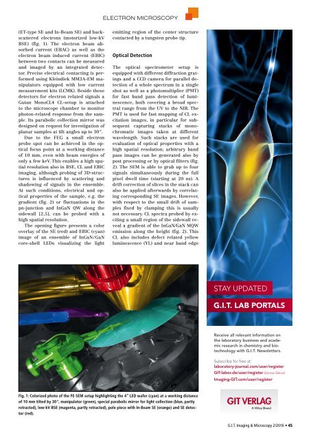
Fig. 1: Colorized photo of the FE-SEM setup highlighting the 4” LED wafer (cyan) at a working distance<br />
of 10 mm tilted by 30 °, manipulator (green), special parabolic mirror for light collection (blue, partly<br />
retracted), low-kV BSE (magenta, partly retracted), pole piece with In-Beam SE (orange) and SE detector<br />
(red).<br />
G.I.T. Imaging & Microscopy 2/2016 • 45