

MINIMUM DIMENSION DIMPLE ANALYSIS - NEPP
MINIMUM DIMENSION DIMPLE ANALYSIS - NEPP
MINIMUM DIMENSION DIMPLE ANALYSIS - NEPP

Create successful ePaper yourself
Turn your PDF publications into a flip-book with our unique Google optimized e-Paper software.
MEMS Reliability Alliance<br />
Technical Report No. 36-02<br />
<strong>MINIMUM</strong> <strong>DIMENSION</strong> <strong>DIMPLE</strong> <strong>ANALYSIS</strong><br />
Gisela Lin, Russell A. Lawton, Joanne Wellman, Leslie Phinney<br />
Jet Propulsion Laboratory<br />
July 14, 2000<br />
The MEMS Reliability Alliance is composed of three core institutions:<br />
(1) MEMScaP S.A., a MEMS software company who provides the MEMS-Pro design<br />
software.<br />
(2) Cronos Integrated Microsystems, a wholly-owned subsidiary of JDS Uniphase.<br />
Cronos provides a polysilicon surface micromachining process (MUMPs) to the<br />
international MEMS community<br />
(3) Jet Propulsion Laboratory, which provides the MEMS test structure design, release<br />
etching, testing, and characterization.<br />
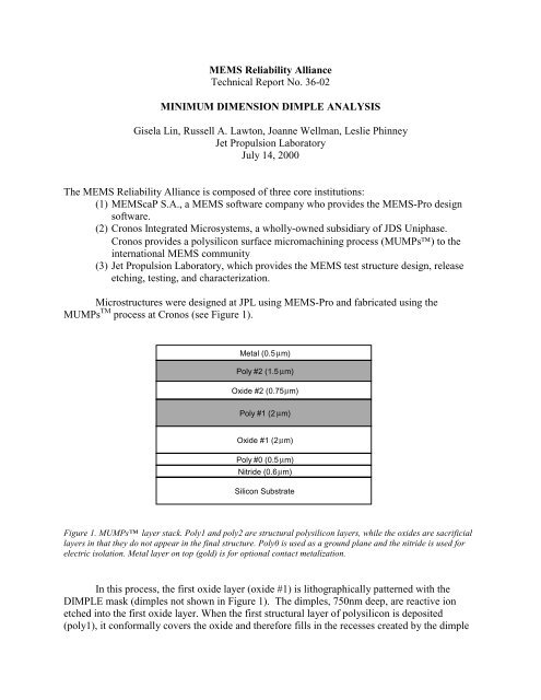
Microstructures were designed at JPL using MEMS-Pro and fabricated using the<br />
MUMPs TM process at Cronos (see Figure 1).<br />
Metal (0.5 µ m)<br />
Poly #2 (1.5 µ m)<br />
Oxide #2 (0.75µ m)<br />
Poly #1 (2 µ m)<br />
Oxide #1 (2µ m)<br />
Poly #0 (0.5 µ m)<br />
Nitride (0.6µ m)<br />
Silicon Substrate<br />
Figure 1. MUMPs layer stack. Poly1 and poly2 are structural polysilicon layers, while the oxides are sacrificial<br />
layers in that they do not appear in the final structure. Poly0 is used as a ground plane and the nitride is used for<br />
electric isolation. Metal layer on top (gold) is for optional contact metalization.<br />
In this process, the first oxide layer (oxide #1) is lithographically patterned with the<br />
<strong>DIMPLE</strong> mask (dimples not shown in Figure 1). The dimples, 750nm deep, are reactive ion<br />
etched into the first oxide layer. When the first structural layer of polysilicon is deposited<br />
(poly1), it conformally covers the oxide and therefore fills in the recesses created by the dimple
etch. Thus, the polysilicon will be closer to the substrate in these areas (see Figure 3). When the<br />
oxides are etched away during the release etch, these recessed areas in the polysilicon are<br />
designed to reduce stiction by minimizing the amount of surface area actually in contact with the<br />
substrate after release. Usually, the dimples are pattered into small squares throughout the poly1<br />
mask to create a periodic array of "bumps" or bushings that lift the majority of the polysilicon<br />
plate 750nm off the substrate.<br />
According to the MUMPS design rules available from Cronos, the minimum feature size<br />
for the dimples is 2µm while the minimum spacing is 3µm. In the MUMPS36 run, minimum<br />
dimension dimples (i.e. 2µm × 2µm) do not appear in the final structure, but 3µm × 3µm dimples<br />
do appear. The test structure used to study this anomaly is a hinged poly1 plate, shown in Figure<br />
2. After release etching the poly1 plate is free to rotate about the poly2 staples anchored to the<br />
substrate (see Figure 3).<br />
Microhinge<br />
Poly1 flip-over<br />
plate with dimples<br />
and etch holes<br />
Poly1 tie-down<br />
Poly1 buckled<br />
beam microjack<br />
Figure 2. Top view of the hinge layout drawn using MEMS-Pro software. Plate dimensions vary from 100um x<br />
100um to 500um x 500um. The tie-down is supposed to be broken after release etching. Microjacks are used to help<br />
lift the poly1 plate -- using a probe the free end is pushed towards the anchored end, buckling the beam, and lifting<br />
the poly1 tab. Then a second probe can then be safely slid under the plate to complete rotation about the hinges.
Figure 3. Cross-section through the hinge, as simulated using MEMS-Pro software. Also shown in this cross section<br />
are both sacrificial oxide layers (oxide 1 and oxide 2) and the silicon nitride layer that covers the whole substrate<br />
for electrical isolation. The dimple layer is also simulated, as shown by the dip in the poly1 layer.<br />
Optical microscope photographs were taken of poly1 plates after release etching. Both<br />
sides were photographed -- i.e. the top side and the bottom side, which became visible once the<br />
plate was rotated 180° about the hinges. Clearly, if the dimples have dimensions 3µm × 3µm in<br />
the MEMS-Pro layout, they were fabricated (see Figure 4 and 5).<br />
40µm<br />
Poly1<br />
hinge-pin<br />
Poly2<br />
staple<br />
Microhinge<br />
Etch hole<br />
Dimple<br />
Dimple<br />
Top surface of a<br />
poly1 plate<br />
Silicon<br />
nitride<br />
Figure 4. Top view of the top surface of an unassembled poly1 plate showing dimples. Although the dimples and<br />
etch holes have the same dimensions in MEMS-Pro (3µm × 3µm square), the etch holes are about 4µm in diameter<br />
and the dimples are about 1 - 1.5µm in diameter. This test structure is different from the one shown in Figure 1.
40µm<br />
Figure 5. Vie w of bottom side of a poly1 plate after rotation about the hinges. The dimples and etch holes have<br />
similar dimensions. In this photograph, some of the dimples in the array are intentionally omitted. This test structure<br />
is different from the one shown in Figure 1 and Figure 4.<br />
Conformal coverage of the 2µm -thick poly1 layer is indicated by the smaller visible<br />
feature on the top surface compared to the bottom surface. The polysilicon is expected to fill in<br />
the patterned hole in oxide1. The sidewalls of the feature may be thicker than 2µm, which would<br />
explain the smaller features on the top surface as shown below:<br />
Poly1<br />
Oxide 1<br />
1µm<br />
4µm<br />
Dimple<br />
Etch hole<br />
Bottom surface of<br />
a poly1 plate<br />
Top surface<br />
Bottom surface<br />
Figure 6. Side view diagram showing conformal coverage of the polysilicon over the recess etched into the oxide.<br />
Recess is 0.75µm deep. Imaging the top and bottom surfaces would produce features of different dimensions.<br />
The test structure shown in Figure 1 was designed in MEMS-Pro such that the etch holes<br />
were 3µm × 3µm and the dimples were 2µm × 2µm. When the MUMPS36 chips came back<br />
from the fabrication facility, the dimples did not appear in the final structure, as shown in Figure<br />
7 and 8. This indicates that either (a) 2µm × 2µm is not the minimum dimension for dimples or<br />
(b) there may be a dimple mask error at the fabrication facility. The 2µm × 2µm dimples are not<br />
being etched into oxide 1.
40µm<br />
Figure 7. Top surface of the polysilicon flap test structure. Etch holes are clearly visible but the dimples are not.<br />
40µm<br />
Figure 8. Bottom surface of the polysilicon flap test structure. Etch holes are clearly visible but the dimples are not.<br />
Conclusions<br />
• According to the MUMPS design rules, the minimum feature size for the dimples is 2µm<br />
while the minimum spacing is 3µm. In the MUMPS36 run, minimum dimension dimples (i.e.<br />
2µm × 2µm) do not appear in the final structure, while 3µm × 3µm dimples do.


![mil-std-2223 [test methods for insulated electric wire] - NEPP](https://img.yumpu.com/4036001/1/190x249/mil-std-2223-test-methods-for-insulated-electric-wire-nepp.jpg?quality=85)