My Curriculum Vitae - Computer Engineering Research Group ...
My Curriculum Vitae - Computer Engineering Research Group ...
My Curriculum Vitae - Computer Engineering Research Group ...
Create successful ePaper yourself
Turn your PDF publications into a flip-book with our unique Google optimized e-Paper software.
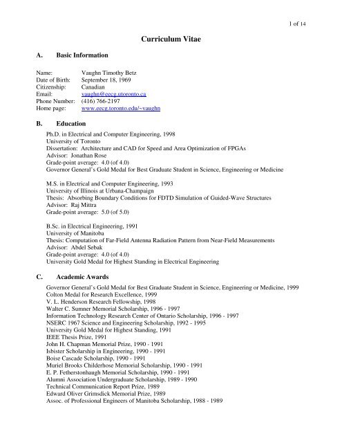
A. Basic Information<br />
Name: Vaughn Timothy Betz<br />
Date of Birth: September 18, 1969<br />
Citizenship: Canadian<br />
Email: vaughn@eecg.utoronto.ca<br />
Phone Number: (416) 766-2197<br />
Home page: www.eecg.toronto.edu/~vaughn<br />
B. Education<br />
<strong>Curriculum</strong> <strong>Vitae</strong><br />
Ph.D. in Electrical and <strong>Computer</strong> <strong>Engineering</strong>, 1998<br />
University of Toronto<br />
Dissertation: Architecture and CAD for Speed and Area Optimization of FPGAs<br />
Advisor: Jonathan Rose<br />
Grade-point average: 4.0 (of 4.0)<br />
Governor General’s Gold Medal for Best Graduate Student in Science, <strong>Engineering</strong> or Medicine<br />
M.S. in Electrical and <strong>Computer</strong> <strong>Engineering</strong>, 1993<br />
University of Illinois at Urbana-Champaign<br />
Thesis: Absorbing Boundary Conditions for FDTD Simulation of Guided-Wave Structures<br />
Advisor: Raj Mittra<br />
Grade-point average: 5.0 (of 5.0)<br />
B.Sc. in Electrical <strong>Engineering</strong>, 1991<br />
University of Manitoba<br />
Thesis: Computation of Far-Field Antenna Radiation Pattern from Near-Field Measurements<br />
Advisor: Abdel Sebak<br />
Grade-point average: 4.0 (of 4.0)<br />
University Gold Medal for Highest Standing in Electrical <strong>Engineering</strong><br />
C. Academic Awards<br />
Governor General’s Gold Medal for Best Graduate Student in Science, <strong>Engineering</strong> or Medicine, 1999<br />
Colton Medal for <strong>Research</strong> Excellence, 1999<br />
V. L. Henderson <strong>Research</strong> Fellowship, 1998<br />
Walter C. Sumner Memorial Scholarship, 1996 - 1997<br />
Information Technology <strong>Research</strong> Center of Ontario Scholarship, 1996 - 1997<br />
NSERC 1967 Science and <strong>Engineering</strong> Scholarship, 1992 - 1995<br />
University Gold Medal for Highest Standing, 1991<br />
IEEE Thesis Prize, 1991<br />
John H. Chapman Memorial Prize, 1990 - 1991<br />
Isbister Scholarship in <strong>Engineering</strong>, 1990 - 1991<br />
Boise Cascade Scholarship, 1990 - 1991<br />
Muriel Brooks Childerhose Memorial Scholarship, 1990 - 1991<br />
E. P. Fetherstonhaugh Memorial Scholarship, 1990 - 1991<br />
Alumni Association Undergraduate Scholarship, 1989 - 1990<br />
Technical Communication Report Prize, 1989<br />
Edward Oliver Grimsdick Memorial Prize, 1989<br />
Assoc. of Professional Engineers of Manitoba Scholarship, 1988 - 1989<br />
1 of 14
Alumni Association Entrance Scholarship for High Standing, 1987 - 1988<br />
Governor General’s Bronze Medal for Highest Standing in High School, 1987<br />
D. Professional Societies<br />
Member of the Institute of Electrical and Eletronics Engineers (IEEE)<br />
Member of the Association of Computing Machinery (ACM)<br />
E. Experience<br />
E.1 Industrial Experience<br />
2 of 14<br />
Senior Director, Software <strong>Engineering</strong>, Altera Toronto Technology Centre: 2008 – May 2011.<br />
In charge of the Altera Toronto site of approximately 90 engineers. In addition to the technical areas for<br />
which I was responsible as a director (please see the 2003 – 2007 entry), I assumed responsibility for the<br />
Quartus II incremental compile, visualization and floorplanning technologies, and (joint with the San<br />
Jose team) responsibity for optimization during Quartus logic synthesis. I was also responsible for the<br />
Altera university program (which creates teaching materials and hardware for use by university digital<br />
logic and computer organization courses), the analysis of our hardware and software vs. that of the<br />
competition, and the development of intellectual property (IP) cores to interface Altera FPGAs to highspeed<br />
memory devices such as DDR3 DRAMs. I drove a major re-architecting of these memory interface<br />
IP cores and the related hardware in our FPGAs to reach higher speeds and achieve lower latency. <strong>My</strong><br />
team developed industry-leading signal integrity analysis tools that are fast, easy-to-use, and accurate.<br />
<strong>My</strong> team continued to improve the algorithms throughout the Quartus II CAD flow, and parallelized six<br />
major Quartus II algorithms – in total, we reduced the compile time for the typical circuit by 6X from<br />
2003 to today, while simultaneously greatly improving result quality. In addition to managing the team, I<br />
continued to play a large role in architecting new CAD techniques and proposing new circuit ideas.<br />
Director, Software <strong>Engineering</strong>, Altera Toronto Technology Centre: January 2003 – December 2007.<br />
During this time my team grew from 23 to 47 research and development engineers. I had overall<br />
responsibility for several key software technologies, including the placement and routing engine, timing<br />
modeling, signal integrity analysis and power estimation for Altera’s Field Programmable Gate Arrays<br />
(FPGAs) and structured ASICs. In concert with engineers in San Jose, my team developed the<br />
architecture of the Stratix II & III and Cyclone II & III FPGA families. We developed new power<br />
modeling and power optimization algorithms and incorporated these algorithms into Altera’s Quartus II<br />
CAD system. <strong>My</strong> team developed the programmable back-bias technology used in Stratix III FPGAs to<br />
reduce the (otherwise high) static power consumption of 65 nm devices. <strong>My</strong> team’s role in delivering<br />
industry-leading <strong>Computer</strong>-Aided Design (CAD) software and device architecture has been a crucial<br />
factor in Altera’s competitiveness.<br />
Senior Manager, Software <strong>Engineering</strong>, Altera Toronto Technology Centre: Jan. 2001 – Dec. 2002.<br />
Led a team that grew during this time from 7 to 14 people, and who were responsible for researching<br />
new placement and routing algorithms and coding the placement and routing engine and related software<br />
support for Altera’s Stratix and Cyclone FPGAs. I architected much of the Quartus II CAD system<br />
support for these FPGAs, and was also one of the architects of the devices themselves.<br />
Manager, Software <strong>Engineering</strong>, Altera Toronto Technology Centre: May 2000 – December 2000.<br />
Led a team of 6 engineers who developed a new placement and routing engine for Altera’s APEX 20K<br />
series of FPGAs. This new engine reduced compile time by 3X while simultaneously increasing circuit<br />
speed by 45%, on average, vs. prior technology. It also greatly improved the routing completion rate,<br />
from approximately 60% to over 95%. This improved placement and routing technology was crucial in
3 of 14<br />
improving Altera’s competitive position, and led Altera to rename their CAD suite from Quartus to<br />
Quartus II to emphasize the new technology it contained.<br />
Co-founder and Vice President of <strong>Engineering</strong>, Right Track CAD, Toronto, ON: Oct. 1998 – May 2000.<br />
I co-founded Right Track CAD to commercialize my doctoral research into place-and-route and FPGA<br />
architecture evaluation CAD tools. I was in charge of overall technical management, and helped grow<br />
the company from four to twelve people. I defined the overall architecture of our software and led a team<br />
of 9 engineers in implementing these CAD tools. Altera replaced the place-and-route engine in their<br />
Max+PlusII CAD suite with the Right Track engine, which achieved an average 30X reduction in<br />
compile time while improving circuit speed by an average of 38% vs. Altera’s existing engine. Cypress<br />
Semiconductor contracted with Right Track to develop their next-generation FPGA architecture. Right<br />
Track was acquired by Altera Corporation in May 2000, and all subsequent Altera FPGAs have been<br />
designed using Right Track’s architecture evaluation CAD tools.<br />
Software Engineer, Integrated <strong>Engineering</strong> Software, Winnipeg, MB: May – Dec. 1991 and May - August<br />
1989 and 1990.<br />
Developed computer-aided engineering software to model electromagnetic phenomena. Ported software<br />
from DOS-based PCs to Unix Workstations, rewrote all graphics and the user interface, and developed<br />
the software’s security system for Unix-based platforms.<br />
E.2 Academic Experience<br />
Associate Professor, University of Toronto: Appointment Commencing July 1, 2011<br />
Adjunct Professor, University of Toronto: July 1, 2009 – present.<br />
Co-supervisor (with Jonathan Rose) of Ph.D. candidate Henry Wong. Early work on this project has<br />
focused on determining how the relative area and speed of various low-level structures that are<br />
commonly used in processors differ between an FPGA and a full-custom implementation.<br />
<strong>Research</strong> Assistant, University of Toronto: 1993 - 1998.<br />
<strong>Research</strong>ed computer-aided design algorithms and improved architectures for Field-Programmable Gate<br />
Array (FPGA) routing and logic blocks. I developed the VPR placement and routing program and the<br />
VPack clustering program to aid in FPGA research; these tools have since been very widely used in both<br />
industry and academia. I created a now-standard FPGA architecture research methodology -- implement<br />
benchmark circuits through a complete parameterized CAD suite that is driven by detailed area and delay<br />
models of the circuitry required by each FPGA.<br />
Lecturer, University of Toronto: Fall semester, 1995 and 1996.<br />
Taught the “Introduction to Microprocessors” course to third-year engineering students for two<br />
consecutive years. Prepared the course outline, lectures, laboratories, all tests and exams, and gave all<br />
lectures. In charge of three laboratory teaching assistants, and rewrote the 150 page lab manual.<br />
Received teaching evaluations well above the department average.<br />
Teaching Assistant, University of Toronto: 1994 - 1998.<br />
Laboratory instructor and grader for undergraduate courses on hardware design with VHDL, physical<br />
electronics, and basic electronics.<br />
<strong>Research</strong> Assistant, University of Illinois at Urbana-Champaign: 1992 - 1993.<br />
Developed improved absorbing boundary conditions to simulate radiation in electro-magnetic<br />
simulations, and integrated these improvements into a finite-difference time-domain simulator for the<br />
analysis of VLSI and printed circuit board interconnect at very high speeds.
E.3 Committees<br />
4 of 14<br />
2002 – 2011: Program Committee of ACM / SIGDA International Symposium on Field-Programmable Gate<br />
Arrays<br />
2005 – 2007: Program Committee of International Conference on Field Programmable Logic and<br />
Applications<br />
2006 – 2011: Program Committee of IEEE International Conference on Field-Programmable Technology<br />
2001 - 2003: Program Committee of IEEE Custom Integrated Circuits Conference<br />
F. Publications<br />
Summary<br />
Books 1<br />
Book Chapters 2<br />
Refereed Papers in Journals 9<br />
Refereed and Invited Papers in Conferences 20<br />
Refereed Papers in Workshops 1<br />
Invited Articles 1<br />
U.S. Patents Granted 61<br />
Software Packages Released 3<br />
Conference Keynotes 2<br />
Conference Panels 2<br />
Invited Presentations at Universities and Companies 9<br />
Internet seminars 5<br />
Citation Count Summary 1<br />
Publications with > 700 citations 2<br />
Publications with between 100 and 699 citations 5<br />
Publications with between 50 and 99 citations 4<br />
Publications with between 20 and 49 citations 7<br />
Books and Book Chapters:<br />
1. V. Betz, J. Rose, and A. Marquardt, Architecture and CAD for Deep-Submicron FPGAs, Kluwer<br />
Academic Publishers, 1999. Citation count: 835.<br />
2. V. Betz, “Placement for General Purpose FPGAs,” Chapter 14, in Reconfigurable Computing, A.<br />
DeHon and S. Hauck, Eds., Morgan Kauffman, 2007, pp. 299 - 317.<br />
3. M. Hutton and V. Betz, "FPGA Synthesis and Physical Design," Volume 1, Chapter 13, in Electronic<br />
Design Automation for Integrated Circuits Handbook, L. Scheffer, L. Lavagno, and G. Martin, Eds.,<br />
Taylor and Francis CRC Press, 2006, pp. 13-1 to 13-32.<br />
Refereed Journal Publications:<br />
1. W. Zhang, V. Betz and J. Rose, “Portable and Scalable FPGA-Based Acceleration of a Direct Linear<br />
System Solver,” To Appear in IEEE Trans. on Reconfigurable Technology and Systems.<br />
1 Citation counts from Google scholar, including citations in both articles and patents, June 23, 2011.
5 of 14<br />
2. A. Ludwin and V. Betz, “Efficient and Deterministic Parallel Placement for FPGAs,” ACM Trans. on<br />
Design Automation of Electronic System, Vol. 16, No. 3, June 2011, pp. 22:1 – 22:23.<br />
3. R. Fung, V. Betz and W. Chow, “Slack Allocation and Routing to Improve FPGA Timing While<br />
Repairing Short-Path Violations,” IEEE Trans. on <strong>Computer</strong>-Aided Design of Circuits and Systems,<br />
April 2008, pp. 686 – 697. Citation count: 1.<br />
4. R. Tessier, V. Betz, D. Neto, A. Egier and T. Gopalsamy, “Power-efficient RAM Mapping Algorithms<br />
for FPGA Embedded Memory Blocks,” IEEE Trans. on <strong>Computer</strong>-Aided Design of Circuits and<br />
Systems, February 2007, pp. 278 - 290. Citation count: 6.<br />
5. A. Marquardt, V. Betz and J. Rose, “Speed and Area Tradeoffs in Cluster-Based FPGA Architectures,”<br />
IEEE Trans. on VLSI Systems, February 2000, pp. 84 - 93. Citation count: 45.<br />
6. V. Betz and J. Rose, “Effect of the Prefabricated Routing Track Distribution on FPGA Area-Efficiency,”<br />
IEEE Trans. on VLSI Systems, Sept. 1998, pp. 445 - 456. Citation count: 30.<br />
7. V. Betz and J. Rose, “How Much Logic Should Go in an FPGA Logic Block?” IEEE Design and Test<br />
Magazine, Spring 1998, pp. 10 - 15. Citation count: 62.<br />
8. V. Betz and R. Mittra, “A Boundary Condition to Absorb Both Propagating and Evanescent Waves in a<br />
Finite-Difference Time-Domain Simulation,” IEEE Transactions on Microwave and Guided Wave<br />
Letters, vol. 3, June 1993, pp. 182 - 184. Citation count: 8.<br />
9. V. Betz and R. Mittra, “Comparison and Evaluation of Boundary Conditions for the Absorption of<br />
Guided waves in an FDTD Simulation,” IEEE Transactions on Microwave and Guided Wave Letters,<br />
vol. 2, pp. 499 - 501, Dec. 1992. Citation count: 31.<br />
Refereed and Invited Conference Papers:<br />
10. H. Wong, J. Rose and V. Betz, “Comparing FPGA vs. Custom CMOS and the Impact on Processor<br />
Microarchitecture,” ACM Int. Symp.on FPGAs, 2011, pp. 5 – 14.<br />
11. S. Brown and V. Betz, “Recent FPGA Advances and Challenges,” 10th Int. Conf. on <strong>Engineering</strong> of<br />
Reconfigurable Systems and Algorithms, 2010, pp. 117 – 120.<br />
12. D. Chen, D. Singh, J. Chromczak, D. Lewis, R. Fung, D. Neto and V. Betz, “A Comprehensive<br />
Approach to Modeling, Characterizing and Optimizing for Metastability in FPGAs,” ACM Int. Symp. on<br />
Field Programmable Gate Arrays, 2010, pp. 167 – 176. Citation count: 1.<br />
13. V. Betz and S. Brown, “FPGA Challenges and Opportunities at 40 nm and Beyond,” International<br />
Conference on Information Electronics Systems, Sendai, Japan, 2009, pp. 141-144. (invited paper)<br />
14. W. Zhang, V. Betz and J. Rose, “Portable and Scalable FPGA-Based Acceleration of a Direct Linear<br />
System Solver,” IEEE Int. Conf. on Field-Programmable Technology, 2008, pp. 17 - 24. Citation count:<br />
6.<br />
15. A. Ludwin, V. Betz and K. Padalia, “High-Quality, Deterministic Parallel Placement for FPGAs on<br />
Commodity Hardware,” ACM / Sigda Int. Symp. on Field Programmable Gate Arrays, 2008, pp. 14 - 23.<br />
Citation count: 23.<br />
16. R. Tessier, V. Betz, D. Neto and T. Gopalsamy, “Power-Aware RAM Mapping for FPGA Embedded<br />
Memory Blocks,” ACM International Symposium on Field Programmable Gate Arrays, 2006, pp. 189 -<br />
198. Citation count: 24.<br />
17. D. Lewis, E. Ahmed, G. Baeckler, V. Betz, M. Bourgeault, D. Cashman, D. Galloway, M. Hutton, C.<br />
Lane, A. Lee, P. Leventis, S. Marquardt, C. McClintock, K. Padalia, B. Pedersen, G. Powell, B. Ratchev,<br />
S. Reddy, J. Schleicher, K. Stevens, R. Yuan, R. Cliff and J. Rose, “The Stratix II Logic and Routing
6 of 14<br />
Architecture,” ACM International Symposium on Field Programmable Gate Arrays, 2005, pp. 14 - 20.<br />
Citation count: 84.<br />
18. R. Fung, V. Betz and W. Chow, “Simultaneous Short-Path and Long-Path Timing Optimization for<br />
FPGAs,” IEEE International Conference on <strong>Computer</strong>-Aided Design, November 2004, 838 - 845.<br />
Citation count: 10.<br />
19. D. Lewis, V. Betz, D. Jefferson, A. Lee, C. Lane, P. Leventis, S. Marquardt, C. McClintock, B.<br />
Pedersen, G. Powell, S. Reddy, C. Wysocki, R. Cliff and J. Rose, “The Stratix Routing and Logic<br />
Architecture,” ACM International Symposium on Field-Programmable Gate Arrays, February 2003, pp.<br />
12 - 20. Citation count: 177.<br />
20. V. Betz and J. Rose, “Automatic Generation of FPGA Routing Architectures from High-Level<br />
Descriptions,” ACM International Symposium on Field Programmable Gate Arrays, Monterey, CA,<br />
February 2000, pp. 175 - 184. Citation count: 39.<br />
21. A. Marquardt, V. Betz and J. Rose, “Timing-Driven Placement for FPGAs,” ACM/SIGDA International<br />
Symposium on Field Programmable Gate Arrays, Monterey, CA, February 2000, pp. 203 - 213. Citation<br />
count: 179.<br />
22. V. Betz and J. Rose, “Circuit Design, Transistor Sizing and Wire Layout of FPGA Interconnect,” IEEE<br />
Custom Integrated Circuits Conference, San Diego, CA, May 1999, pp. 171 - 174. Citation count: 47.<br />
23. V. Betz and J. Rose, “FPGA Routing Architecture: Segmentation and Buffering to Optimize Speed and<br />
Density,” ACM Int. Symp. on Field Programmable Gate Arrays, Monterey, CA, pp. 59 – 68, 1999.<br />
Citation count: 114.<br />
24. A. Marquardt, V. Betz and J. Rose, “Using Cluster-Based Logic Blocks and Timing-Driven Packing to<br />
Improve FPGA Speed and Density,” ACM Int. Symp. on Field Programmable Gate Arrays, Monterey,<br />
CA, pp. 37 – 46, 1999. Citation count: 148.<br />
25. J. Swartz, V. Betz and J. Rose, “A Fast Routability-Driven Router for FPGAs,” ACM Int. Symp. on Field<br />
Programmable Gate Arrays, Monterey, CA, pp. 140 - 149, 1998. Citation count: 84.<br />
26. V. Betz and J. Rose, “Cluster-Based Logic Blocks for FPGAs: Area-Efficiency vs. Input Sharing and<br />
Size,” IEEE Custom Integrated Circuits Conference, Santa Clara, CA, pp. 551 - 554, 1997. Citation<br />
count: 100.<br />
27. V. Betz and J. Rose, “Directional Bias and Non-Uniformity in FPGA Global Routing Architectures,”<br />
IEEE/ACM International Conference on <strong>Computer</strong>-Aided Design, San Jose, CA, pp. 652 - 659, 1996.<br />
Citation count: 76.<br />
28. V. Betz and J. Rose, “Using Architectural Families to Increase FPGA Speed and Density,” ACM<br />
International Conference on Field-Programmable Gate Arrays, Monterey, CA, pp. 10 - 16, 1995.<br />
Citation count: 11.<br />
29. V. Betz, N. P. East, and A. Sebak, “Applications of Planar Near-Field Measurements to Electromagnetic<br />
Radiation and Interference Problems,” Canadian Conference on Electrical and <strong>Computer</strong> <strong>Engineering</strong>,<br />
Montreal, PQ, pp. 72.1.1 - 72.1.4, 1991.<br />
Refereed Workshop Papers:<br />
30. V. Betz and J. Rose, “VPR: A New Packing, Placement and Routing Tool for FPGA <strong>Research</strong>,” Seventh<br />
International Workshop on Field-Programmable Logic and Applications, London, UK, pp. 213 - 222,<br />
1997. Citation count: 736.
Invited Articles:<br />
7 of 14<br />
31. V. Betz, “FPGAs, Programming Models and Kit Cars,” The Last Byte article, To Appear in IEEE Design<br />
and Test of <strong>Computer</strong>s.<br />
United States Patents Granted: 2<br />
1. G. Lai, A. Lee, R. Fung, V. Betz and A. LeBlanc, “Clock Switch-Over Circuits and Methods,” U.S.<br />
Patent #7,911,240, Filed May 17, 2007, Issued March 22, 2011.<br />
2. D. Neto, V. Betz, M. Varia and G. Baeckler, “Method and Apparatus for Deriving Signal Activities for<br />
Power Analysis and Optimization”, U.S. Patent #7,877,710, Filed May 1, 2006, Issued Jan. 25, 2011.<br />
3. R. Tessier, V. Betz, T. Golpalsamy, and D. Neto, “Power-Aware RAM Processing,” U.S. Patent<br />
#7,877,555, Filed Aug. 24, 2006, Issued Jan. 25, 2011.<br />
4. Y. Kretchmer, P. Leventis and V. Betz, “Power-Driven Timing Analysis and Placement for<br />
Programmable Logic”, U.S. Patent #7,861,190, Filed March 17, 2005, Issued Dec. 28, 2010.<br />
5. R. Fung, V. Betz and D. Karchmer, “Method and Apparatus for Performing Path-Level Skew<br />
Optimization and Analysis for a Logic Design,” U.S. Patent #7,853,911, Filed Nov. 4, 2005, Issued Dec.<br />
14, 2010.<br />
6. V. Betz, C. Pantofaru, and J. Swartz, “Method and Apparatus for Utilizing Constraints for the Routing of<br />
a Design on a Programmable Logic Device,” U.S. Patent #7,757,197, Filed May 29, 2003, Issued July<br />
13, 2010.<br />
7. G. Lai, A. Lee, R. Fung and V. Betz, “Periphery Clock Distribution Network for a Programmable Logic<br />
Device,” U.S. Patnet #7,737,751, Filed Jan. 30, 2007, Issued June 15, 2010.<br />
8. R. Fung and V. Betz, “Optimizing Long-Path and Short-Path Timing and Accounting for Manufacturing<br />
and Operating Condition Variability (Part 3),” U.S. Patent #7,725,853, Filed Sept. 18, 2007, Issued May<br />
25, 2010.<br />
9. T. Vanderhoek, V. Betz, D. Cashman, D. Lewis, M. Hutton, “Programamble Logic Device Architectures<br />
and Methods for Implementing Logic in those Architectures (Part 2),” U.S. Patent #7,716,623, Filed Oct.<br />
15, 2009, Issued May 11, 2010.<br />
10. K. Padalia, K. Bozman and V. Betz, “Techniques for <strong>Group</strong>ing Circuit Elements into Logic Blocks (Part<br />
2),” U.S. Patent #7,707,532, Filed Aug. 23, 2007, Issued April 27, 2010.<br />
11. D. Lewis, P. Leventis, A. Lee, H. Kim, B. Pedersen, C. Wysocki, C. Lane, A. Marquardt, V. Santurkar,<br />
and V. Betz, “Versatile Logic Element and Logic Array Block (Part 2),” U.S. Patent #7,671,626, Filed<br />
Aug. 29, 2008, Issued March 2, 2010.<br />
12. R. Fung and V. Betz, “Efficient Delay Elements, (Part 2)” U.S. Patent #7,659,764, Filed Sept. 17, 2008,<br />
Issued Feb. 9, 2010.<br />
13. D. Lewis, P. Leventis, V. Betz, T. Wong, A. Lee, and P. Pan, “Distributed Memory in Field-<br />
Programmable Gate Array Integrated Circuit Devices (Part 2),” U.S. Patent #7.656,191, Filed May 30,<br />
2008, Issued Feb. 2, 2010.<br />
14. R. Fung and V. Betz, “Efficient Delay Elements, (Part 1)” U.S. Patent #7,629,825, Filed Oct. 13, 2006,<br />
Issued Dec. 8, 2009.<br />
2 Other U.S. patents are pending, but are not listed. Some patents have issued internationally as well, but are not listed.
8 of 14<br />
15. T. Vanderhoek, V. Betz, D. Cashman, D. Lewis, M. Hutton, “Programamble Logic Device Architectures<br />
and Methods for Implementing Logic in those Architectures (Part 1),” U.S. Patent #7,619,443, Filed Feb.<br />
16, 2006, Issued Nov. 17, 2009.<br />
16. T. Borer, I. Chesal, J. Schleicher, D. Mendel, M. Hutton, B. Ratchev, Y. Sankar, B. van Antwerpen, G.<br />
Baeckler, R. Yuan, S. Brown, V. Betz and K. Chan, “Techniques for Automated Sweeping of Parameters<br />
in <strong>Computer</strong>-Aided Design to Achieve Optimum Performance and Resource Usage (Part 2),” U.S. Patent<br />
#7,594,208, Filed Dec. 13, 2006, Issued Sept. 22, 2009.<br />
17. A. Lee, C. McClintock, B. Johnson, R. Cliff, S. Reddy, C. Lane, P. Leventis, V. Betz and D. Lewis,<br />
“PLD Architecture for Flexible Placement of IP Function Blocks,” Filed Aug. 12, 2005, Issued Sept. 1,<br />
2009.<br />
18. D. Lewis, V. Betz, R. Irfan, P. McElheny, Y.-J. Liu, and B. Pedersen, “Apparatus and Methods for<br />
Adjusting Performance of Integrated Circuits,” U.S. Patent #7,573,317, Filed Sept. 26, 2006, Issued Aug.<br />
11, 2009.<br />
19. I. Milton, D. Neto and V. Betz, “<strong>Computer</strong>-Aided-Design Tools for Reducing Power Consumption in<br />
Programmable Logic Devices,” U.S. Patent #7,555,741, Filed Sept. 13, 2006, Issued June 30, 2009.<br />
20. D. Mendel and V. Betz, “Systems and Methods for Reducing Static and Total Power Consumption in<br />
Programmable Logic Device,” (Part 2), U.S. Patent #7,467,314, Filed Dec. 19, 2006, Issued Dec. 16,<br />
2008.<br />
21. T. Borer, D. Karchmer, J. Govig, A. Leaver, G. Quan, K. Chan, V. Betz and S. Brown, “Method and<br />
Apparatus for Performing Incremental Compilation,” U.S. Patent #7,464,362, Filed March 20, 2006,<br />
Issued Dec. 9, 2008.<br />
22. K. Padalia, V. Betz and V. Gouterman, “Methods for Designing Integrated Circuits,” U.S. Patent<br />
#7,441,208, Filed Sept. 13, 2005, Issued Oct. 21, 2008.<br />
23. D. Lewis, P. Leventis, A. Lee, H. Kim, B. Pedersen, C. Wysocki, C. Lane, A. Marquardt, V. Santurkar,<br />
and V. Betz, “Versatile Logic Element and Logic Array Block (Part 1),” U.S. Patent #7,432,734, Filed<br />
May 2, 2007, Issued Oct. 7, 2008.<br />
24. K. Padalia, J. Peters, and V. Betz, “Automatic Adjustment of Optimization Effort in Configuring<br />
Programmable Devices,” U.S. Patent #7,415,682, Filed April 1, 2005, Issued Aug. 19, 2008.<br />
25. V. Gouterman, V. Betz, and M. Bourgeault, “Method and Apparatus for Performing Integrated Global<br />
Routing and Buffer Insertion,” U.S. Patent #7,412,680, Filed Sept. 15, 2005, Issued Aug. 12, 2008.<br />
26. D. Lewis, C. Lane, S. Sribhashyam, S. Perisetty, T. Vanderhoek, V. Betz, T. Wong, and A. Lee,<br />
“Apparatus and Methods for Optimizing the Performance of Programmable Logic Devices,” U.S. Patent<br />
#7,400,167, Filed Aug 16, 2005, Issued July 15, 2008.<br />
27. D. Lewis, V. Betz, P. Leventis, C. Lane, A. Lee, J. Watt, and T. Vanderhoek, “Apparatus and Methods<br />
for Power Management in Integrated Circuits,” U.S. Patent #7,405,589, Filed Dec.22, 2005, Issued July<br />
29, 2008.<br />
28. J. Yuan, C. Lane, D. Jefferson, and V. Betz, “Flexible RAM Clock Enable,” U.S. Patent #7,397,296,<br />
Filed April 7, 2006, Issued July 8, 2008.<br />
29. D. Lewis, P. Leventis, V. Betz, T. Wong, A. Lee and P. Pan, “Distributed Memory in Field-<br />
Programmable Gate Array Integrated Circuit Devices (Part 1),” U.S. Patent #7,391,236, Filed Dec. 27,<br />
2005, Issued June 24, 2008.<br />
30. D. Lewis and V. Betz, “Error Correction for Programmable Logic Integrated Circuits,” U.S. Patent<br />
#7,328,377, Filed Jan. 27, 2004, Issued Feb. 5, 2008.
9 of 14<br />
31. R. Fung, V. Betz and W. Chow, “Method and Apparatus for Utilizing Long-Path and Short-Path Timing<br />
Constraints in an Electronic-Design-Automation Tool for Routing,” (Part 2), U.S. Patent #7,308,664,<br />
Filed Feb. 9, 2004, Issued Dec. 11, 2007.<br />
32. D. Lewis, P. Leventis, and V. Betz, “Distributed Random Access Memory in a Programmable Logic<br />
Device,” (Part 2), U.S. Patent #7,304,499, Filed June 16, 2006, Issued Dec. 4, 2007.<br />
33. R. Fung and V. Betz, “Optimizing Long-Path and Short-Path Timing and Accounting for Manufacturing<br />
and Operating Condition Variability,” (Part 2), U.S. Patent #7,290,232, Filed December 1, 2004, Issued<br />
Oct. 30, 2007.<br />
34. D. Mendel and V. Betz, “Systems and Methods for Reducing Static and Total Power Consumption in<br />
Programmable Logic Device Architectures,” U.S. Patent #7,287,171, Filed March 8, 2004, Issued Oct.<br />
23, 2007.<br />
35. K. Padalia, K. Bozman and V. Betz, “Techniques for <strong>Group</strong>ing Circuit Elements into Logic Blocks (Part<br />
1),” U.S. Patent #7,275,288, Filed Nov. 17, 2003, Issued Sept. 25, 2007.<br />
36. R. Fung and V. Betz, “Optimizing Long-Path and Short-Path Timing and Accounting for Manufacturing<br />
and Operating Condition Variability,” (Part 1), U.S. Patent #7,254,789, Filed December 1, 2004, Issued<br />
August 7, 2007.<br />
37. M. Hutton and V. Betz, “Swap Mux to Relieve Logic Device Input Line Stress,” U.S. Patent #7,248,072,<br />
Filed Feb. 11, 2004, Issued July 24, 2007.<br />
38. D. Lewis, P. Leventis, A. Lee, H. Kim, B. Pedersen, C. Wysocki, C. Lane, A. Marquardt, V. Santurkar,<br />
and V. Betz, “Versatile Logic Element and Logic Array Block,” U.S. Patent #7,218,133, Filed Feb. 2,<br />
2005, Granted May 15, 2007.<br />
39. R. Fung, V. Betz and W. Chow, “Method and Apparatus for Utilizing Long-Path and Short-Path Timing<br />
Constraints in an Electronic-Design-Automation Tool for Routing,” (Part 1), U.S. Patent #7,207,020,<br />
Filed Feb. 9, 2004, Issued April 17, 2007.<br />
40. A. Lee, N. Ngo, V. Betz, D. Lewis, B. Pederson, J. Schleicher, “Bypass-able Carry Chain in a<br />
Programmable Logic Device,” U.S. Patent #7,205,791, Filed March 12, 2004, Issued April 17, 2007.<br />
41. T. Borer, G. Quan, S. Brown, D. Singh, C. Sanford, V. Betz, C. Pantofaru, J. Swartz, “Method and<br />
Apparatus for Implementing Soft Constraints in Tools Used for Designing Systems on Programmable<br />
Logic Devices,” U.S. Patent #7,194,720, Filed July 11, 2003, Issued March 20, 2007.<br />
42. D. Mendel and V. Betz, “Systems and Methods for Reducing Static and Total Power Consumption in<br />
Programmable Logic Device,” (Part 1), U.S. Patent #7,188,266, Filed March 8, 2004, Issued March 6,<br />
2007.<br />
43. T. Borer, I. Chesal, J. Scheicher, D. Mendel, M. Hutton, B. Ratchev, Y. Sankar, B. van Antwerpen, G.<br />
Baeckler, R. Yuan, S. Brown, V. Betz, K. Chan, “Techniques for Automated Sweeping of Parameters in<br />
<strong>Computer</strong>-Aided Design to Achieve Optimum Performance and Resource Usage (Part 1),” U.S. Patent<br />
#7,181,703, Filed July 22, 2003, Issued Feb. 20, 2007.<br />
44. A. Lee, G. Lai, C. Zhang, V. Betz and R. Fung, “Variable Delay Circuitry,” U.S. Patent #7,138,844,<br />
Filed March 18, 2005, Issued Nov. 21, 2006.<br />
45. D. Lewis, V. Betz, I. Rahim, P. McElheny, and Y.-J. Liu, “Apparatus and Methods for Adjusting<br />
Performance of Integrated Circuits,” U.S. Patent #7,129,745, Filed June 10, 2004, Issued Oct. 31, 2006.<br />
46. D. Lewis, P. Leventis, and V. Betz, “Distributed Random Access Memory in a Programmable Logic<br />
Device,” (Part 1), U.S. Patent #7,084,665, Filed July 22, 2004, Issued Aug. 1, 2006.
10 of 14<br />
47. A. Lee, N. Ngo, V. Betz, D. Lewis, B. Pedersen, and J. Schleicher, “Initializing a Carry Chain in a<br />
Programmable Logic Device,” U.S. Patent #7,061,268, Filed March 15, 2004, Issued June 13, 2006.<br />
48. A. Lee, C. McClintock, B. Johnson, R. Cliff, S. Reddy, C. Lane, P. Leventis, V. Betz, and D. Lewis,<br />
“Methods for Designing PLD Architectures for Flexible Placement of IP Function Blocks,” U.S. Patent<br />
#7,058,920, Filed June 11, 2003, Issued June 6, 2006.<br />
49. V. Betz and J. Rose, “Automatic Generation of Programmable Logic Device Architectures,” (Part 2),<br />
U.S. Patent #7,051,313, Filed Aug. 13, 2003, Issued May 23, 2006.<br />
50. D. Lewis, P. Leventis, A. Lee, B. Johnson, R. Cliff, S. Reddy, C. Lane, C. McClintock, V. Betz, C.<br />
Wysocki, and A. Mardquardt, “Routing Architecture for a Programmable Logic Device,” Filed July 21,<br />
2003, Issued Nov. 29, 2005.<br />
51. V. Betz, E. Ahmed, and D. Neto, “Techniques for Identifying Functional Blocks in a Design that Match<br />
a Template and Combining the Functional Blocks into Fewer Programmable Circuit Elements,” U. S.<br />
Patent #6,957,412, Filed Nov. 15, 2002, Issued Oct. 18, 2005.<br />
52. D. Lewis, P. Leventis, A. Lee, H. Kim, B. Pedersen, C. Wysocki, C. Lane, A. Mardquardt, V. Santurkar,<br />
and V. Betz, “Versatile Logic Element and Logic Array Block,” U.S. Patent #6,937,064, Filed Oct. 24,<br />
2002, Issued Aug. 30, 2005.<br />
53. D. Lewis, V. Betz, P. Leventis, M. Chan, C. McClintock, A. Lee, C. Lane, S. Reddy, and R. Cliff,<br />
“System and Method for Optimizing Routing Lines in a Programmable Logic Device,” Filed Jan. 25,<br />
2002, Issued May 17, 2005.<br />
54. V. Betz and J. Rose, “Heterogenous Interconnection Architecture for Programmable Logic Devices,”<br />
(Part 2), U.S. Patent #6,828,824, Filed May 30, 2003, Issued Dec. 7, 2004.<br />
55. B. Johnson, A. Lee, C. McClintock, T. Nguyen, D. Jefferson, P. Leventis, D. Lewis, V. Betz, and M.<br />
Chan, “Flexible I/O Routing Resources,” U.S. Patent #6,826,741, Filed Nov. 6, 2002, Issued Nov. 30,<br />
2004.<br />
56. V. Betz and D. Galloway, “Method of Optimizing the Design of Electronic Systems Having Multiple<br />
Timing Constraints,” Filed Feb. 23, 2001, Issued July 13, 2004.<br />
57. V. Betz and J. Rose, “Automatic Generation of Programmable Logic Device Architectures,” (Part 1),<br />
U.S. Patent #6,631,510, Filed Oct. 29, 1999, Issued Oct. 7, 2003.<br />
58. D. Lewis, P. Leventis, A. Lee, B. Johnson, R. Cliff, S. Reddy, C. Lane, C. McClintock, V. Betz, C.<br />
Wysocki, and A. Mardquardt, “Routing Architecture for a Programmable Logic Device,” U.S. Patent<br />
#6,630,842, Filed May 6, 2002, Issued Oct. 7, 2003.<br />
59. A. Lee, C. McClintock, B. Johnson, R. Cliff, S. Reddy, C. Lane, P. Leventis, V. Betz, D. Lewis, “PLD<br />
Architecture for Flexible Placement of IP Function Blocks,” U.S. Patent #6,605,962, Filed Jan. 25, 2002,<br />
Issued Aug. 12, 2003.<br />
60. V. Betz and J. Rose, “Heteregenous Interconnection Architecture for Programmable Logic Devices,”<br />
U.S. Patent #6,590,419, Filed Oct. 12, 1999, Issued July 8, 2003.<br />
61. J. Rose and V. Betz, “Complementary Architectures for Field-Programmable Gate Arrays,” U.S. Patent<br />
#5,537,341, filed Feb. 10, 1995, Issued July 16, 1996.<br />
Software Packages Developed and Released<br />
1. VPR + VPack: Versatile packing, placement and routing for FPGAs. This CAD tool allows for very<br />
general exploration of FPGA architecture, and has also obtained very high-quality CAD results against<br />
which other tools are often benchmarked. Used by over 182 companies and 1000 university researchers.<br />
Incoporated into the SPEC2000 CPU benchmark suite.
11 of 14<br />
2. Quartus University Interface Program (QUIP): I drove the development of QUIP, which documents<br />
interfaces in and out of the Quartus II CAD system that allow academic researchers to integrate and test<br />
their algorithms or CAD tools within a complete commercial CAD system. This system has been<br />
extensively used by the academic community.<br />
3. EasyGL: An easy-to-use graphics library that supports X11 and PostScript output, and handles all<br />
windowing, redrawing, and coordinate transformations. Ported to Win32 by subsequent graduate<br />
students and professors. Used in several universities as a graphics library for research and graduate<br />
courses.<br />
Conference Keynotes:<br />
1. “FPGAs at 28 nm: Meeting the Challenge of Modern Systems-on-a-Chip,” IEEE International<br />
Conference on Field Programmable Logic and Applications, Milan, Italy, 2010.<br />
2. “FPGA Challenges and Opportunities at 40 nm and Beyond,” IEEE International Conference on Field<br />
Programmable Logic and Applications, Prague, Czech Republic, 2009.<br />
Conference Panels:<br />
3. Participant in Pre-Conference Workshop, ACM/SIGDA International Symposium on FPGAs, “Grand<br />
Challenges in FPGA <strong>Research</strong>,” Monterey, CA, 2007.<br />
4. Participant in Panel, ACM/SIGDA International Symposium on FPGAs, “Will Power Kill FPGAs?,”<br />
Monterey, CA, 2006.<br />
Invited Presentations at Universities and Companies:<br />
5. “Real Life Software <strong>Engineering</strong>: How to Deliver Software that Works.” Described how to create highquality<br />
and maintainable software, especially when the system is large and complex.<br />
• University of Toronto, Jan. 2010 and Jan. 2011<br />
• University of Waterloo, Jan. 2011.<br />
6. “FPGA Technology and Trends.” An overview of how FPGAs work, how they compare to other<br />
methods of implementing electronic systems, and some of the trends and challenges in the<br />
semiconductor industry.<br />
• University of Natural Sciences, Ho Chi Minh City, Vietnam, Nov. 2008.<br />
• University of Technology, Ho Chi Minh City, Vietnam, Nov. 2008.<br />
7. “The Stratix III and IV FPGA Architectures.” Described architectural advances in Altera’s 65 and 40 nm<br />
high-end FPGA families, and the analyses and experimentation behind these advances. The topics<br />
covered included the adaptive logic module, programmable power (regional back-bias) power<br />
management, routing and memory architecture improvements, and future challenges for FPGAs.<br />
• Imperial College, London, UK, July 2008.<br />
8. “Large Scale Design and Project Management.” Laid out principles I have found useful to ensure<br />
complex designs and projects stay focused, on schedule and achieve high quality and performance.<br />
Illustrated these principles with 3 case studies from my experience, ranging from a team of 4 developing<br />
a new CAD system to a team of 300 engineers developing a new FPGA and all the associated software.<br />
• Guest lecture to ECE 298 (<strong>Engineering</strong> Design class), University of Toronto, presented in 2004,<br />
2005, 2006 and 2007.<br />
• Seminar at University of Manitoba, Nov. 2006.
12 of 14<br />
9. “CAD and Architecture for FPGAs and Structured ASICs: Recent Results and Open Challenges.”<br />
Presented an overview of recent FPGA and structured ASIC research and products, and highlighted the<br />
most important research challenges I see ahead.<br />
• University of Waterloo, Nov. 2006.<br />
• University of Manitoba, Oct. 2006.<br />
10. “From <strong>Research</strong> to Reality: One Start-Up’s Story.” A case study of the business decisions I faced as I<br />
commercialized my PhD research by founding a start-up, especially the choice of business model,<br />
intellectual property rights, growth strategy and exit strategy.<br />
• University of California, Berkeley, Nov. 2010.<br />
• University of Manitoba, Oct. 2009.<br />
• Schulich School of Business, Toronto, ON, presented in April 2003 and March 2004.<br />
11. “From Concept to Silicon: the Altera Stratix FPGA.” Described the new virtual prototyping<br />
methodology used to develop the Stratix FPGA family, highlighted the key research results in routing<br />
and logic architecture found during development, and presented an overview of the final architecture.<br />
• Imperial College, London, UK, June 2003.<br />
• University of British Columbia, March 2003.<br />
• University of Toronto, Feb. 2003.<br />
• University of Manitoba, Feb. 2003.<br />
12. “Cluster-Based Logic Blocks for FPGAs: Area-Efficiency vs. Input Sharing and Size.” Presented<br />
research results from my PhD examining how to create the most area-efficient FPGA logic blocks.<br />
• Xilinx Inc., San Jose, CA., 1997<br />
• Altera Corp. San Jose, CA., 1997<br />
• Actel Inc., San Jose, CA, 1997<br />
13. “Global Routing Architectures for FPGAs.” Presented research results from my PhD concerning how to<br />
best distribute routing resources across an FPGA die.<br />
• Fourth Canadian Workshop on Field-Programmable Devices, Toronto, ON, 1996.<br />
• Xilinx Inc., San Jose, CA., 1996<br />
• Altera Corp. San Jose, CA., 1996<br />
• Actel Inc., San Jose, CA, 1996<br />
Internet Seminars:<br />
14. V. Betz and S. Verma, “Manage Performance and Power Using 40 nm FPGAs,”<br />
http://www.altera.com/education/webcasts/all/wc-2008-perf-power-40nm-fpga.html, Internet Seminar,<br />
July 2008.<br />
Described the new features in the Stratix IV FPGA families that impact power and performance,<br />
including strained silicon, regional back-bias, high-speed serial transceiver architecture and DDR3<br />
memory interface circuitry.<br />
15. V. Betz and S. Rajput, “Learn to Design with Stratix III FPGAs’ Programmable Power Technology and<br />
Selectable Core Voltage,” http://www.altera.com/education/webcasts/all/wc-2007-stratix3-designpower-voltage.html,<br />
Internet Seminar, March 2007.<br />
Detailed the major power management hardware features in Stratix III FPGAs, and how the Quartus II<br />
CAD system automatically exploits them.<br />
16. V. Betz, “Using Stratix III FPGAs to Achieve Higher Performance Systems with Lower Power,”<br />
http://www.techonline.com/learning/livewebinar/500004, Internet Seminar, Dec. 2006.<br />
Introduced the new features in the Stratix III architecture, including programmable power, signal<br />
integrity enhancements and a new RAM architecture.
13 of 14<br />
17. V. Betz and S. Rajput, “Reduce FPGA Power With Automatic Optimization & Power-Efficient Design,”<br />
http://www.techonline.com/learning/webinar/62100187, Internet Seminar, Nov. 2005.<br />
Explained the algorithms in the Quartus II CAD system that automatically optimize RAM, logic, routing<br />
and clocking power, and presented data on their effectiveness. Described power-efficient design<br />
techniques.<br />
18. V. Betz and P. Ekas, “Power Solutions for Leading-Edge FPGAs,” Internet Seminar, March 2005.<br />
Explained the impact of 90 nm process technology on power, best practices for power estimation, and the<br />
techniques used to control power in Altera’s Stratix II FPGAs and HardCopy structured ASICs.<br />
G. Other Skills and Projects:<br />
• Designed, laid out, verified and tested a 60 000 transistor, 1.2 µm full-custom time-domain multiplexing<br />
and packetizing chip (in a five-member team). Developed netlist translation programs, Cadence skill<br />
scripts and verification strategies to create a complete design and verification flow. First silicon was<br />
fully functional.<br />
• Fabricated a 2 inch semiconductor wafer, performing all lithography, diffusion etc. steps, and<br />
characterized the fabricated devices.<br />
• Programming languages: C, C++, Fortran, 68K assembly, VHDL, Verilog.<br />
• Commercial CAD system experience: very extensive knowledge of Quartus II FPGA design software,<br />
solid knowledge of HSPICE, experience with ASIC CAD flows.<br />
• Extensive experience writing VLSI CAD tools, electromagnetic simulation software, graphics and data<br />
visualization applications.<br />
• Considerable knowledge of computer architecture, graphics hardware, and memory design.<br />
H. References:<br />
Dr. Jonathan Rose<br />
Professor<br />
Department of Electrical and <strong>Computer</strong> <strong>Engineering</strong><br />
University of Toronto<br />
10 King’s College Road<br />
Toronto, ON<br />
CANADA<br />
M5S 3G4<br />
Phone: (416) 978-6992<br />
Fax: (416) 978-1145<br />
Email: jayar@eecg.toronto.edu<br />
Dr. Jason Cong<br />
Professor<br />
Department of <strong>Computer</strong> Science<br />
UCLA<br />
4731J, Boelter Hall<br />
Los Angeles, CA 90095<br />
U.S.A.<br />
Phone: (310) 206-2775<br />
Fax: (310) 825-2273
Email: cong@cs.ucla.edu<br />
Dr. Russell Tessier<br />
Associate Professor<br />
Department of Electrical and <strong>Computer</strong> <strong>Engineering</strong><br />
University of Massachusetts<br />
309G Knowles <strong>Engineering</strong> Building<br />
Amherst, MA 01003<br />
U.S.A.<br />
Phone: (413) 545-0160<br />
Fax: (413) 545-1993<br />
Email: tessier@ecs.umass.edu<br />
Additional references available on request.<br />
14 of 14


