

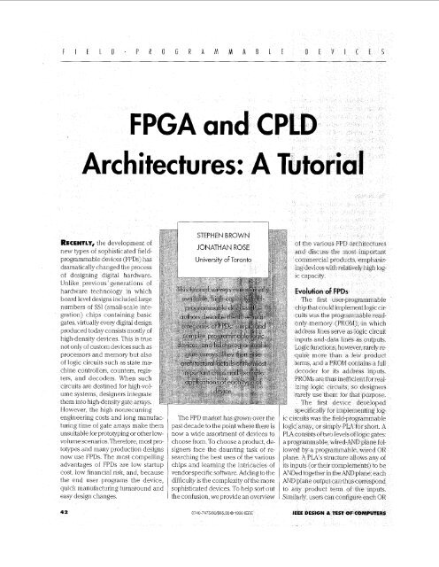
FPGA a:nd CPLD Architectures: A Tutorial - IEEE Design & Test of ...
FPGA a:nd CPLD Architectures: A Tutorial - IEEE Design & Test of ...
FPGA a:nd CPLD Architectures: A Tutorial - IEEE Design & Test of ...

Create successful ePaper yourself
Turn your PDF publications into a flip-book with our unique Google optimized e-Paper software.
F I E L D - P R O G R A M M A B L E<br />
RECENTLY, the development <strong>of</strong><br />
new types <strong>of</strong> sophisticated fieldprogrammable<br />
devices (FPDs) has<br />
dramatically changed the process<br />
<strong>of</strong> designing digital hardware.<br />
Unlike previous' generations <strong>of</strong><br />
hardware technology in which<br />
board level designs included large<br />
numbers <strong>of</strong> SSI (small-scale integration)<br />
chips containing basic<br />
gates, virtually every digital design<br />
produced today consists mostly <strong>of</strong><br />
high-density devices. This is true<br />
not only <strong>of</strong> custom devices such as<br />
processors a<strong>nd</strong> memory but also<br />
<strong>of</strong> logic circuits such as state machine<br />
controllers, counters, registers,<br />
a<strong>nd</strong> decoders When such<br />
circuits are destined for high-volume<br />
systems, designers integrate<br />
them into high-density gate arrays.<br />
However, the high nonrecurring<br />
engineering costs a<strong>nd</strong> long manufacturing<br />
time <strong>of</strong> gate arrays make them<br />
unsuitable for prototyping or other lowvolume<br />
scenarios. Therefore, most prototypes<br />
a<strong>nd</strong> many production designs<br />
now use FPDs. The most compelling<br />
advantages <strong>of</strong> FPDs are low startup<br />
cost, low financial risk, a<strong>nd</strong>, because<br />
the e<strong>nd</strong> user programs the device,<br />
quick manufacturing turnarou<strong>nd</strong> a<strong>nd</strong><br />
easy design changes.<br />
42<br />
difficulty is the complex1<br />
sophisticated devices.<br />
the confusion, we prov<br />
0740-7475/96/$05 00 0 1996 <strong>IEEE</strong>
Inputs a<strong>nd</strong> flip-flop<br />
feedbacks<br />
Figure 7. PAL structure.<br />
utputs<br />
plane output to produce the logical<br />
sum <strong>of</strong> any AND plane output. With this<br />
structure, PLAs are well-suited for im-<br />
plementing logic functions in sum-<strong>of</strong>-<br />
products form. They are also quite<br />
versatile, Since both the AND a<strong>nd</strong> OR<br />
terms can have many inputs (product<br />
literature <strong>of</strong>ten calls this feature “wide<br />
AND a<strong>nd</strong> OR gates”).<br />
When Philips introduced PLAs in the<br />
early 1970s, their main drawbacks were<br />
expense <strong>of</strong> manufacturing a<strong>nd</strong> some-<br />
what poor speed performance. Both<br />
disadvantages arose from the two lev-<br />
els <strong>of</strong> configurable logic; programma-<br />
ble logic planes were difficult to<br />
manufacture a<strong>nd</strong> introduced significant<br />
propagation delays. To overcome these<br />
weaknesses, Monolithic Memories<br />
(MMI, later merged with Advanced<br />
Micro Devices) developed PAL devices.<br />
As Figure 1 shows, PALS feature only a<br />
single level <strong>of</strong> programmability-a pro-<br />
grammable, wired-AND plane that<br />
feeds fixed-OR gates. To compensate<br />
for the lack <strong>of</strong> generality incurred by the<br />
fixed-OR plane, PALS come in variants<br />
with different numbers <strong>of</strong> inputs a<strong>nd</strong><br />
outputs a<strong>nd</strong> various sizes <strong>of</strong> OR gates.<br />
To implement sequential circuits, PALS<br />
usually contain flip-flops connected to<br />
the OR gate outputs.<br />
The introduction <strong>of</strong> PAL devices pro-<br />
fou<strong>nd</strong>ly affected digital hardware de-<br />
sign, a<strong>nd</strong> they are the basis <strong>of</strong> some <strong>of</strong><br />
the newer, more sophisticated archi-<br />
tectures that we will describe shortly.<br />
Variants <strong>of</strong> the basic PAL architecture<br />
appear in several products known by<br />
FPDs, including PLAs, PALS, a<strong>nd</strong> PAL<br />
like devices, into the single category <strong>of</strong><br />
simple programmable-logic devices<br />
SUMMER 1996 43
F I E L D - P R O G R A M M A<br />
44
Switch type Reprogramma ble? Volatile? Technology<br />
Fuse<br />
EPROM<br />
EEPROM<br />
S M<br />
Anti fuse<br />
No<br />
Yes<br />
(out <strong>of</strong> circuit)<br />
Yes<br />
(in circuit)<br />
Yes<br />
(in circuit)<br />
No<br />
are floating gate transistors like those<br />
used in EPROM (erasable programma-<br />
ble read-only memoiy) a<strong>nd</strong> EEPROM<br />
(electrically erasable PROM). For<br />
<strong>FPGA</strong>s, they are SRAM (static RAM) a<strong>nd</strong><br />
antifuse. Table 1 lists the most impor-<br />
tant characteristics <strong>of</strong> these program-<br />
ming technologies.<br />
To use an EPROM or EEPROM tran-<br />
sistor as a programmable switch for<br />
<strong>CPLD</strong>s (a<strong>nd</strong> many SPLDs), the manu-<br />
facturer places the transistor between<br />
two wires to facilitate implementation<br />
<strong>of</strong> wired-AND functions. Figure 4 shows<br />
EPROM transistors connected in a<br />
<strong>CPLD</strong>’s AND plane. An input to the AND<br />
plane can drive a product wire to logic<br />
level 0 through an EPROM transistor, if<br />
that input is part <strong>of</strong> the correspo<strong>nd</strong>ing<br />
product term. For inputs not involved<br />
in a product term, the appropriate<br />
EPROM transistors are programmed as<br />
permanently turned <strong>of</strong>f. The diagram <strong>of</strong><br />
an EEPROM-based device would look<br />
similar to the one in Figure 4.<br />
Although no technical reason pre-<br />
vents application <strong>of</strong> EPROM or EEP-<br />
ROM to <strong>FPGA</strong>s, current commercial<br />
<strong>FPGA</strong> products use either SRAM or an-<br />
tifuse technologies. The example <strong>of</strong><br />
SRAM-controlled switches in Figure 5 il-<br />
lustrates two applications, one to con-<br />
trol the gate nodes <strong>of</strong> pass-transistor<br />
switches a<strong>nd</strong> the other, the select lines<br />
<strong>of</strong> multiplexers that drive logic block in-<br />
puts. The figure shows the connection<br />
<strong>of</strong> one logic block (represented by the<br />
SUMMER 1996<br />
Product<br />
No Bipolar wire<br />
No UVCMOS<br />
No EECMOS<br />
Yes CMOS I<br />
I<br />
I EPROM I EPROM<br />
CMOS+ Figure 4. EPROM programmable<br />
switches.<br />
7 I I- I<br />
I I I<br />
I I I<br />
Figure 5. SRAM-controlled programmable switches.<br />
AND gate in the upper left comer) to an-<br />
other through two pass-transistor<br />
switches a<strong>nd</strong> then a multiplexer, all<br />
controlled by SRAM cells. Whether an<br />
<strong>FPGA</strong> uses pass transistors, multiplex-<br />
ers, or both depe<strong>nd</strong>s on the particular<br />
product.<br />
Antifuses are originally open circuits<br />
that take on low resistance only when<br />
programmed. Antifuses are manufac-<br />
tured using modified CMOS technolo-<br />
gy. As an example, Figure 6 (next page)<br />
depicts Actel’s PLICE (programmable<br />
logic interconnect circuit element), an<br />
tifuse structure.’ The antifuse, posi-<br />
tioned between two interconnect wires,<br />
consists <strong>of</strong> three sa<strong>nd</strong>wiched layers:<br />
co<strong>nd</strong>uctors at top a<strong>nd</strong> bottom a<strong>nd</strong> an<br />
insulator in the middle. Unpro-<br />
grammed, the insulator isolates the top<br />
a<strong>nd</strong> bottom layers; programmed, the in-<br />
sulator becomes a low-resistance link.<br />
11<br />
I<br />
45
F I E L D - P R O G R A M M A B L<br />
ctel's PLICE antifuse structure<br />
Figure 7. CAD process for SPLDs.<br />
Fix errors<br />
Programming unit<br />
PLICE uses polysilicon a<strong>nd</strong> n+ diffusion<br />
as co<strong>nd</strong>uctors a<strong>nd</strong> a custom-developed<br />
compou<strong>nd</strong>, ONO (oxide-nitride-ox-<br />
insulator. Other antifuses<br />
eta1 for co<strong>nd</strong>uctors, with<br />
amorphous silicon as the middle lay-<br />
er.2,3<br />
CAD for FPDs<br />
Computer-aided design programs are<br />
essential in designing circuits for im-<br />
plementation in FPDs Such s<strong>of</strong>tware<br />
tools are important not only for<br />
a<strong>nd</strong> <strong>FPGA</strong>s, but also for<br />
cal CAD system for SPLD<br />
ware for the following tasks: initial<br />
design entry, logic optimization, device<br />
fitting, simulation, a<strong>nd</strong> configuration.<br />
Figure 7 illustrates the SPLD design<br />
process. To enter a design, the designer<br />
creates a schematic diagram with a<br />
graphical CAD tool, describes the de-<br />
sign in a simple hardware description<br />
46<br />
Automatic<br />
language, or combines these<br />
Since initial logic entry is not usually in<br />
an optimized form, the s<br />
algorithms to optimize<br />
Then additional algorithms<br />
resulting logic equations<br />
into the SPLD. Simulation<br />
rect operation, a<strong>nd</strong> the designer returns<br />
to the design entry step<br />
When a design simulates<br />
designer loads it into a pr<br />
can accommodate large d<br />
more common to use diffe<br />
I
o<strong>nd</strong>-sourced by other companies. The<br />
designation 16R8 means that the PAL<br />
has a maximum <strong>of</strong> 16 inputs (eight ded-<br />
icated inputs a<strong>nd</strong> eight input/outputs)<br />
a<strong>nd</strong> a maximum <strong>of</strong> eight outputs, a<strong>nd</strong><br />
that each output is registered (R) by a D<br />
flip-flop. Similarly, the 22V10 has a max-<br />
imum <strong>of</strong> 22 inputs a<strong>nd</strong> ten outputs. The<br />
V meansversatile-that is, each output<br />
can be registered or combinational.<br />
Another widely used a<strong>nd</strong> seco<strong>nd</strong>-<br />
sourced SPLD is the Altera Classic<br />
EP610. This device is similar in com-<br />
plexity to PALS, but <strong>of</strong>fers more flexibil-<br />
ity in the production <strong>of</strong> outputs a<strong>nd</strong> has<br />
larger AND a<strong>nd</strong> OR planes. The EPGlOs<br />
outputs can be registered, a<strong>nd</strong> the flip-<br />
flops are configurable as D, T, JK, or SR.<br />
Many other SPLD products are avail-<br />
able from a wide array <strong>of</strong> companies.<br />
All share common characteristics such<br />
as logic planes (AND, OR, NOR, or<br />
NAND), but each <strong>of</strong>fers unique features<br />
suitable for particular applications. A<br />
partial list <strong>of</strong> companies that <strong>of</strong>fer SPLDs<br />
includes AMD, Altera, ICT, Lattice,<br />
Cypress, a<strong>nd</strong> Philips-Signetics. The com-<br />
plexity <strong>of</strong> some <strong>of</strong> these SPLDs ap-<br />
proaches that <strong>of</strong> <strong>CPLD</strong>s.<br />
<strong>CPLD</strong>s. As we said earlier, <strong>CPLD</strong>s<br />
consist <strong>of</strong> multiple SPLD-like blocks on<br />
a single chip. However, <strong>CPLD</strong> products<br />
are much more sophisticated than<br />
SPLDs, even at the level <strong>of</strong> their basic<br />
SPLD-like blocks. In the following de-<br />
scriptions, we present sufficient details<br />
to compare competing products, em-<br />
phasizing the most widely used devices.<br />
Altera Max. Altera has developed<br />
three families <strong>of</strong> <strong>CPLD</strong> chips: Max 5000,<br />
7000, a<strong>nd</strong> 9000. We focus on the 7000<br />
series because <strong>of</strong> its wide use a<strong>nd</strong> state-<br />
<strong>of</strong>-the-art logic capacity a<strong>nd</strong> speed per-<br />
formance. Max 5000 represents an older<br />
technology that <strong>of</strong>fers a cost-effective<br />
solution; Max 9000 is similar to Max<br />
7000 but <strong>of</strong>fers higher logic capacity<br />
(the i<strong>nd</strong>ustry's highest for <strong>CPLD</strong>s). ' '<br />
Figure 8 depicts the general archi-<br />
SUMMER 1996<br />
I10<br />
block<br />
PIA<br />
gure 8. Ahera Max 7000 series architecture.<br />
PIA<br />
Array <strong>of</strong> 16<br />
macrocells<br />
A<br />
gure 9. Ahera Max 7000 logic array block.<br />
cture <strong>of</strong> the Altera Max 7000 series. It<br />
Insists <strong>of</strong> an array <strong>of</strong> logic array blocks<br />
id a set <strong>of</strong> interconnect wires called a<br />
.ogrammable interconnect array<br />
'IA). The PIA can connect any logic<br />
ray block input %r output to any 0th-<br />
logic array block. The chip's inputs<br />
Logc<br />
array<br />
,I block<br />
-<br />
To I/O cells<br />
a<strong>nd</strong> outputs connect directly to the PIA<br />
a<strong>nd</strong> to logic array blocks. A logic array<br />
block is a complex, SPLD-like structure,<br />
a<strong>nd</strong> so we can consider the entire chip<br />
an array <strong>of</strong> SPLDs.<br />
Figure 9 showsthe structure <strong>of</strong> a log-<br />
ic array block. Each logic array block<br />
47
F I E L D - P R O G R A M M A B L E<br />
Local logic I<br />
array block<br />
interconnect<br />
Figure 10. Max 7000 macrocell.<br />
Figure 11. AMD Mach 4 structure<br />
consists <strong>of</strong> two sets <strong>of</strong> eight macrocells<br />
(shown in Figure 10). A macrocell is a<br />
rogrammable product terms<br />
(part <strong>of</strong> an AND plane) that feeds an OR<br />
gate a<strong>nd</strong> a flip-flop. The flip-flops can<br />
be D, JK, T, or SR, or can be transpar-<br />
As Figure 10 shows, the product se-<br />
matrix allows avariable number <strong>of</strong><br />
inputs to the OR gate in a macrocell.<br />
48<br />
110 (32)<br />
Any or all <strong>of</strong><br />
the m<br />
ic arr<br />
bility makes the Max 7000 s<br />
efficient in chip area than cla<br />
bec<br />
mo<br />
To PIA f-
etween this block a<strong>nd</strong> a normal PAL<br />
1) a product term (PT) allocator be-<br />
tween the AND plane a<strong>nd</strong> the macro-<br />
cells (the macrocells comprise an OR<br />
gate, an EXOR gate, a<strong>nd</strong> a flip-flop), a<strong>nd</strong><br />
2) an output switch matrix between the<br />
OR gates a<strong>nd</strong> the I/O pins. These fea-<br />
tures make a Mach 4 chip easier to use<br />
because they decouple sections <strong>of</strong> the<br />
PAL-like block. More specifically, the<br />
product term allocator distributes a<strong>nd</strong><br />
shares product terms from the AND<br />
plane to OR gates that require them, al-<br />
lowing much more flexibility than the<br />
fixedsize OR gates in regular PALS. The<br />
output switch matrix enables any<br />
macrocell output (OR gate or flip-flop)<br />
to drive any I/O pin connected to the<br />
PAL-like block, again providing greater<br />
flexibility than a PAL, in which each<br />
macrocell can drive only one specific<br />
I/O pin. Mach 4’s combination <strong>of</strong> insy5<br />
tem programmability a<strong>nd</strong> high flexibil-<br />
ity allow easy hardware design changes.<br />
Lattice pLSI a<strong>nd</strong> ispLSI. Lattice <strong>of</strong>fers<br />
a complete range <strong>of</strong> <strong>CPLD</strong>s, with two<br />
main product lines: the pLSI a<strong>nd</strong> the<br />
isplsI. Each consists <strong>of</strong> three families <strong>of</strong><br />
EEPROM <strong>CPLD</strong>s with different logic ca-<br />
pacities a<strong>nd</strong> speed performance. The<br />
ispLSI devices are insystem program-<br />
mable.<br />
Lattice’s earliest generation <strong>of</strong> <strong>CPLD</strong>s<br />
is the pLSI a<strong>nd</strong> ispLSI 1000 series. Each<br />
chip consists <strong>of</strong> a collection <strong>of</strong> SPLD-<br />
like blocks a<strong>nd</strong> a global routing pool to<br />
connect the blocks. Logic capacity<br />
ranges from about 1,200 to 4,000 gates,<br />
a<strong>nd</strong> pin-to-pin delays are 10 ns. Lattice<br />
also <strong>of</strong>fers the 2000 series-relatively<br />
small <strong>CPLD</strong>s with between 600 a<strong>nd</strong><br />
2,000 gates. The 2000 series features a<br />
higher ratio <strong>of</strong> macrocells to I/O pins<br />
a<strong>nd</strong> higher speed performance than the<br />
1000 series. At 5.5-ns pin-to-pin delays,<br />
the 2000 series provides state-<strong>of</strong>-the-art<br />
speed.<br />
Lattice’s 3000 series consists <strong>of</strong> the<br />
company’s largest <strong>CPLD</strong>s, with up to<br />
5,000 gates a<strong>nd</strong> 10- to 15-ns pin-to-pin<br />
Figure 12. Mach 4 34V16 PAl-like block.<br />
m . I...........<br />
Figure 73. lattice plSl a<strong>nd</strong> isplSl architecture.<br />
jelays. Compared with the chips dis-<br />
xssed so far, the functionality <strong>of</strong> the<br />
3000 series is most similar to that <strong>of</strong> the<br />
Uach 4. Unlike the other Lattice <strong>CPLD</strong>s,<br />
he 3000 series <strong>of</strong>fers enhancements to<br />
juppoit more recent design styles, such<br />
3s <strong>IEEE</strong> Std 1149.1 bou<strong>nd</strong>aly scan.<br />
Figure 13 shows the general structure<br />
3f a Lattice pLSI or ispLSI device.<br />
$rou<strong>nd</strong> the chip’s outside edges are<br />
%directional I/Os, which connect to<br />
30th the generic logic blocks a<strong>nd</strong> the<br />
global routing pool. As the magnified<br />
Jiew on the right side <strong>of</strong> the figure<br />
jhows, the generic logic blocks are<br />
I10 (8)<br />
small PAL-like blocks consisting <strong>of</strong> an<br />
AND plane, a product term allocator,<br />
a<strong>nd</strong> macrocells. The global routing<br />
pool is a set <strong>of</strong> wires that span the chip<br />
to connect generic logic block inputs<br />
a<strong>nd</strong> outputs. All interconnects pass<br />
through the global routing pool, so tim-<br />
ing between logic levels is fully pre-<br />
dictable, as it is for the AMD Mach<br />
devices.<br />
Cypress Flash370. Cypress has re-<br />
cently developed <strong>CPLD</strong> products simi-<br />
lar to the AMD a<strong>nd</strong> Lattice devices in<br />
several ways. Cypress Flash370 <strong>CPLD</strong>s<br />
SUMMER 1996 49
F I E L D - P R O G R A M M A B L E<br />
110s<br />
110s<br />
110s<br />
clot; (4)<br />
l10s I/OS<br />
_-- _-- __--<br />
_*--,,<br />
__.-__<br />
-,----<br />
32 (macrocells --.,<br />
,' a<strong>nd</strong> I10 pins) '\<br />
-' I<br />
I/O<br />
I/O<br />
110<br />
I/O<br />
-, ,, - 0-16 kputs<br />
'*\<br />
,I OR, bypassable<br />
,,,' (D, T, latch)<br />
--- -_____- -. flip-flop,<br />
tristate buffer<br />
Figure 14. Cypress Flash370 architecture. (PIM: programmable interconnect matrix,.)<br />
Data in<br />
Address<br />
Control<br />
Clock<br />
Data out<br />
Figure 15. Altera Flashlogic <strong>CPLD</strong>: general architecture (a); CFB in PAL mode {b]; CFB<br />
in SRAM mode [c)<br />
use flash EEPROM technology a<strong>nd</strong> <strong>of</strong>-<br />
fer speed performance <strong>of</strong> 8.5 to 15 ns<br />
pin-to-pin delays. The Flash370s are not<br />
in-system programmable. To meet the<br />
needs <strong>of</strong> larger chips, the devices pro-<br />
vide more I/O pins than competing<br />
products, with a linear relationship be-<br />
tween the number <strong>of</strong> macrocells a<strong>nd</strong><br />
the number <strong>of</strong> bidirectional<br />
50<br />
The smallest parts have 32 macrocells<br />
a<strong>nd</strong> 32 I/O pins; the largest have 256<br />
macrocells a<strong>nd</strong> 256 pins.<br />
Figure 14 shows that Flas<br />
a typical <strong>CPLD</strong> architectu<br />
ple PAL-like blocks connecte<br />
grammable interconnect
all other <strong>CPLD</strong>s: Instead <strong>of</strong> containing<br />
AND/OR logic, a CFB can serve as a<br />
IO-ns SRAM block. Figure 15b shows a<br />
CFB configured as a PAL, a<strong>nd</strong> Figure<br />
15c shows another configured as an<br />
SRAM. In the SRAM configuration, the<br />
PAL block becomes a 128-word by 10-<br />
bit read/write memory. Inputs that<br />
would normally feed the AND plane in<br />
the PAL become address lines, data<br />
lines, or control signals for the memo-<br />
ry. Flip-flops a<strong>nd</strong> tristate buffers are still<br />
available in the SRAM configuration.<br />
In the Flashlogic device, the AND/OR<br />
logic plane's configuration bits are<br />
SRAM cells connected to EPROM or<br />
EEPROM cells. Applying power loads<br />
the SRAM cells with a copy <strong>of</strong> the non-<br />
volatile EPROM or EEPROM, but the<br />
SRAM cells control the chip's configu-<br />
ration. The user can reconfigure the<br />
chips in system by downloading new in-<br />
formation into the SRAM cells. The user<br />
can make the SRAM cell reprogram-<br />
ming nonvolatile by writing the SRAM<br />
cell contents back to the EPROM cells.<br />
ICT PEEL Arrays. ICT PEEL (pro-<br />
grammable, electrically-erasable logic)<br />
Arrays are large PLAs that include logic<br />
macrocells with flop-flops a<strong>nd</strong> feed-<br />
back to the logic planes. Figure 16 il-<br />
lustrates this structure, which consists<br />
<strong>of</strong> a programmable AND plane that<br />
feeds a programmable OR plane. The<br />
OR plane's outputs are partitioned into<br />
groups <strong>of</strong> four, a<strong>nd</strong> each group can be<br />
input to any <strong>of</strong> the logic cells. The log-<br />
ic cells provide registers for the sum<br />
terms a<strong>nd</strong> can feed back the sum terms<br />
to the AND plane. Also, the logic cells<br />
connect sum terms to I/O pins.<br />
Because they have a PLA-like struc-<br />
ture, the logic capacity <strong>of</strong> PEEL Arrays<br />
is difficult to measure compared to the<br />
<strong>CPLD</strong>s discussed so far, but we estimate<br />
a capacity <strong>of</strong> 1,600 to 2,800 equivalent<br />
gates. Containing relatively few I/O pins,<br />
the largest PEEL Array comes in a 40-pin<br />
package. Since they do not consist <strong>of</strong><br />
SPLD-like blocks, PEEL Arrays do not fit<br />
SUMMER 1996<br />
El-<br />
Input<br />
pins<br />
terms<br />
I/O<br />
&<br />
pins<br />
U<br />
'Group <strong>of</strong> four<br />
sum terms<br />
Figure 76. ICT PEEL Array architecture<br />
well into the <strong>CPLD</strong> category.<br />
Nevertheless, we include them here be<br />
cause they exemplify PLA-based (rather<br />
than PAL-based) devices a<strong>nd</strong> <strong>of</strong>fer larg-<br />
er capacity than a typical SPLD.<br />
The PEEL Array logic cell, shown in<br />
Figure 17, includes a flip-flop, config-<br />
urable as D, T, or JK, a<strong>nd</strong> two multi-<br />
plexers. Each multiplexer produces a<br />
logic cell output, either registered or<br />
combinational. One logic cell output<br />
can connect to an I/O pin, a<strong>nd</strong> the oth-<br />
er output is buried. An interesting fea-<br />
ture <strong>of</strong> the logic cell is that the flip-flop<br />
clock, preset, a<strong>nd</strong> clear are full sum-<strong>of</strong>-<br />
product logic functions. Distinguishing<br />
PEEL Arrays from all other <strong>CPLD</strong>s,<br />
which simply provide product terms for<br />
these signals, this feature is attractive for<br />
some applications. Because <strong>of</strong> their<br />
PLA-like OR plane, PEEL Arrays are es-<br />
pecially well suited to applications that<br />
require very wide sum terms.<br />
<strong>CPLD</strong> applications. Their high<br />
speeds a<strong>nd</strong> wide range <strong>of</strong> capacities<br />
make <strong>CPLD</strong>s useful for many applications,<br />
from implementing ra<strong>nd</strong>om glue<br />
logic to prototyping small gate arrays.<br />
An important reason for the growth <strong>of</strong><br />
the <strong>CPLD</strong> market is the conversion <strong>of</strong><br />
designs that consist <strong>of</strong> multiple SPLDs<br />
into a smaller number <strong>of</strong> <strong>CPLD</strong>s.<br />
<strong>CPLD</strong>s can realize complex designs<br />
such as graphics, LAN, a<strong>nd</strong> cache controllers.<br />
As a rule <strong>of</strong> thumb, circuits that<br />
Four<br />
sum A+.-$-<br />
erms<br />
I Global reset<br />
Figure 77. ICJ PEEL Array logic cell<br />
structure.<br />
:an exploit wide AND/OR gates a<strong>nd</strong> do<br />
iot need a large number <strong>of</strong> flip-flops are<br />
good ca<strong>nd</strong>idates for <strong>CPLD</strong> implemen-<br />
ation. Finite state machines are an ex-<br />
:ellent example <strong>of</strong> this class <strong>of</strong> circuits.<br />
4 significant advantage <strong>of</strong> <strong>CPLD</strong>s is that<br />
hey allow simple design changes<br />
hrough reprogramming (all commer-<br />
5al <strong>CPLD</strong> products are reprogramma-<br />
de). In-system programmable <strong>CPLD</strong>s<br />
?veri make it possible to reconfigure<br />
iardware (for example, change a pro-<br />
ocol for a communications circuit)<br />
Nithout powering down.<br />
<strong>Design</strong>s <strong>of</strong>ten partition naturally into<br />
he SPLD-like blocks in a <strong>CPLD</strong>, pro-<br />
jucing more predictable speed perfor-<br />
nance than a design split into many<br />
small pieces mapped into different ar-<br />
?as <strong>of</strong> the chip. Predictability <strong>of</strong> circuit<br />
mplementation is one <strong>of</strong> the strongest<br />
idvantages <strong>of</strong> <strong>CPLD</strong> architectures.<br />
<strong>FPGA</strong>s. As one <strong>of</strong> the fastest growing<br />
segments <strong>of</strong> the semico<strong>nd</strong>uctor i<strong>nd</strong>us-<br />
ry, the <strong>FPGA</strong> marketplace is volatile.<br />
rhe pool <strong>of</strong> companies involved<br />
Zhanges rapidly, a<strong>nd</strong> it is difficult to say<br />
Nhich products will be most significant<br />
Nhen the i<strong>nd</strong>ustry reaches a stable<br />
state. We focus here on products cur-<br />
cently in widespread use. In describing<br />
2ach device, we list its capacity in two-<br />
nput NAND gates as given by the ven-<br />
joy. Gate count is an especially<br />
zontentious issue in the <strong>FPGA</strong> i<strong>nd</strong>ustry,<br />
md so the numbers given should not<br />
3e taken too seriously. In fact, wags<br />
51
F I E l<br />
channels<br />
not shown<br />
D - P R 0 G R<br />
Figure 19. Xihx XC4000 wire segments.<br />
have coined the term “d<br />
erence to the <strong>of</strong>ten-cited ratio between<br />
human a<strong>nd</strong> dog years, to i<strong>nd</strong>icate the<br />
52<br />
or antifuse-base<br />
c1 c2 G3 e4<br />
-<br />
A M M<br />
A<br />
__ __<br />
Xilinx <strong>FPGA</strong>s. Xilinx FP<br />
array-based structure, eac
short wire segments that span a single<br />
CLB (the number <strong>of</strong> segments in each<br />
channel varies for each member <strong>of</strong> the<br />
XC4000 family), longer segments that<br />
span two CLBs, a<strong>nd</strong> very long segments<br />
that span the chip’s entire length or<br />
width. Programmable switches are<br />
available (see Figure 5) to connect CLB<br />
inputs a<strong>nd</strong> outputs to the wire segments<br />
or to connect one wire segment to an-<br />
other. A small section <strong>of</strong> an XC4000<br />
routing channel appears in Figure 19.<br />
The figure shows only the wire seg-<br />
ments in a horizontal channel-not the<br />
vertical routing channels, CLB inputs<br />
a<strong>nd</strong> outputs, a<strong>nd</strong> the routing switches.<br />
An important point about the Xilinx in-<br />
terconnect is that signals must pass<br />
through switches to reach one CLB<br />
from another, a<strong>nd</strong> the total number <strong>of</strong><br />
switches traversed depe<strong>nd</strong>s on the par-<br />
ticular set <strong>of</strong> wire segments used. Thus,<br />
an implemented circuit’s speed perfor-<br />
mance depe<strong>nd</strong>s in part on how CAD<br />
tools allocate the wire segments to in-<br />
dividual signals.<br />
Altera Flex 8000 a<strong>nd</strong> Flex 10K.<br />
Altera’s Flex 8000 series combines<br />
<strong>FPGA</strong> a<strong>nd</strong> <strong>CPLD</strong> technologies. The de-<br />
vices consist <strong>of</strong> a three-level hierarchy<br />
much like that <strong>of</strong> <strong>CPLD</strong>s. However, the<br />
lowest level <strong>of</strong> the hierarchy is a set <strong>of</strong><br />
lookup tables, rather than an SPLDlike<br />
block, a<strong>nd</strong> so we categorize the Flex<br />
8000 as an <strong>FPGA</strong>. The SRAM-based Flex<br />
8000 features a four-input lookup table<br />
as its basic logic block. Logic capacity<br />
<strong>of</strong> the 8000 series ranges from about<br />
4,000 to more than 15,000 gates.<br />
Figure 20 illustrates the overall Flex<br />
8000 architecture. The basic logic<br />
block, called a logic element, contains<br />
a four-input lookup table, a flip-flop,<br />
a<strong>nd</strong> special-purpose carry circuitry for<br />
arithmetic circuits (similar to the Xilinx<br />
XC4000). The logic element also in-<br />
cludes cascade circuitry that allows ef-<br />
ficient implementation <strong>of</strong> wide AND<br />
functions. Figure 21 shows details <strong>of</strong> the<br />
logic element.<br />
SUMMER 1996<br />
Logic array block i<br />
Figure 20. Ahera Flex 8000 architecture.<br />
Figure 2 I. Flex 8000 logic element.<br />
This design groups logic elements into<br />
sets <strong>of</strong> eight, called logic array blocks (a<br />
term borrowed from Altera’s <strong>CPLD</strong>s). As<br />
shown in Figure 22 on the next page,<br />
each logic array block contains local in-<br />
terconnection, a<strong>nd</strong> each local wire can<br />
connect any logic element to any other<br />
logic element within the same logic ar-<br />
ray block. The local interconnect also<br />
connects to the Flex 8000’s FastTrack<br />
global interconnect. Like the long wires<br />
n...nn...n n...n<br />
in the Xllinx XC4000, each FastTrack wire<br />
exte<strong>nd</strong>s the full width or height <strong>of</strong> the de<br />
vice. However, a major difference be-<br />
tween Flex 8000 a<strong>nd</strong> Xilinx chips is that<br />
FastTrack consists only <strong>of</strong> long lines,<br />
making the Flex 8000 easy for CAD tools<br />
to configure automatically. All FastTrack<br />
horizontal wires are identical. Therefore,<br />
interconnect delays in the Flex 8000 are<br />
more predictable than in <strong>FPGA</strong>s that<br />
employ many shorter segments because<br />
53
F I E L D - P R O G R A M M A B L E<br />
From<br />
FastTrac k<br />
interconnect Control Cascade, carry<br />
Figure 22. Flex 8000 logic array block.<br />
Figure 24. AT&T ORCA p<br />
function unit.<br />
the longer paths cont<br />
grammable switches. Moreover, con-<br />
nections between horizontal a<strong>nd</strong> vertical<br />
lines pass through active buffers, further<br />
enhancing predicta<br />
The Flex 10K fam<br />
able-size blocks <strong>of</strong> S<br />
ded array blocks As<br />
block to serve as<br />
54<br />
3<br />
Figure<br />
AT&T ORCA. AT&T's
units based on the original ORCA<br />
architecture.<br />
Actel FfGAs. Actel <strong>of</strong>fers three main<br />
<strong>FPGA</strong> families: Act 1, Act 2, a<strong>nd</strong> Act 3.<br />
Although the three generations have<br />
similar features, we focus on the most<br />
recent devices. Unlike the <strong>FPGA</strong>s de-<br />
scribed so far, Actel’s devices use anti-<br />
fuse technology a<strong>nd</strong> a structure similar<br />
to traditional gate arrays. Their design<br />
arranges logic blocks in rows with hor-<br />
izontal routing channels between adja-<br />
cent rows (Figure 25). Actel logic<br />
blocks, based on multiplexers, are<br />
small compared to those based on<br />
lookup tables. Figure 26 illustrates the<br />
Act 3 logic block, which consists <strong>of</strong> an<br />
AND a<strong>nd</strong> an OR gate connected to a<br />
multiplexer-based circuit block. In com-<br />
bination with the two logic gates, the<br />
arrangement <strong>of</strong> the multiplexer circuit<br />
enables a single logic block to realize a<br />
wide range <strong>of</strong> functions. About half the<br />
logic blocks in an Act 3 device also con-<br />
tain a flip-flop.<br />
Actel’s horizontal routing channels<br />
consist <strong>of</strong> various-length wire segments<br />
with antifuses to connect logic blocks<br />
to wire segments or one wire to anoth-<br />
er. Although not shown in Figure 25,<br />
vertical wires also overlie the logic<br />
blocks, forming signal paths that span<br />
multiple rows. The speed performance<br />
<strong>of</strong> Actel chips is not fully predictable be<br />
cause the number <strong>of</strong> antifuses traversed<br />
by a signal depe<strong>nd</strong>s on how CAD tools<br />
allocate the wire segments during cir-<br />
cuit implementation. However, a rich<br />
selection <strong>of</strong> wire segment lengths in<br />
each channel a<strong>nd</strong> algorithms that guar-<br />
antee strict limits on the number <strong>of</strong> an-<br />
tifuses traversed by any two-point<br />
connection improve speed perfor-<br />
mance significantly.<br />
Quicklogic pASZC. Actel’s main com-<br />
petitor in antifuse-based <strong>FPGA</strong>s is<br />
Quicklogic, which has two device fam-<br />
ilies, PASIC a<strong>nd</strong> pASIC2. The pASIC, il-<br />
lustrated in Figure 27a, has similarities<br />
Routing<br />
channels<br />
n<br />
I/O blocks<br />
U U<br />
I I/O blocks<br />
Figure 25. Actel <strong>FPGA</strong> structure.<br />
to several other <strong>FPGA</strong>s: Like Xilinx<br />
<strong>FPGA</strong>s, it has an array-based structure;<br />
like Actel <strong>FPGA</strong>s, its logic blocks use<br />
multiplexers; a<strong>nd</strong> like Altera Flex 8OOOs,<br />
its interconnect consists only <strong>of</strong> long<br />
lines. The pASIC2 is a recently intro-<br />
duced enhanced version, which we will<br />
not discuss here. Cypress also <strong>of</strong>fers de-<br />
vices using the pASlC architecture, but<br />
we discuss only Quicklogic’s version.<br />
Quicklogic’s ViaLink antifuse struc-<br />
ture (see Figure 27b) consists <strong>of</strong> a metal<br />
top layer, an amorphoussilicon insulat-<br />
-0 o~ ... n<br />
U<br />
U<br />
. .<br />
...<br />
...<br />
...<br />
...<br />
...<br />
. .<br />
block<br />
Multiplexer-based<br />
Inputs circuit block * output<br />
Inputs<br />
Figure 26. Actel Act 3 logic module.<br />
-<br />
U<br />
U<br />
0<br />
ViaLink . . at every<br />
: : Loaic cell i i . .<br />
wire<br />
crossing<br />
...<br />
... - - U uu<br />
110 blocks<br />
[a) (b)<br />
Figure 27. Quicklogic pASlC structure (aj a<strong>nd</strong> ViaLink (bj.<br />
SUMMER 1996 55<br />
Metal 1
F I E L D - P R O G R<br />
AZ<br />
B1 oz<br />
B2<br />
c1<br />
c2<br />
QZ<br />
D1<br />
D2<br />
El<br />
E2 NZ<br />
F5<br />
F6<br />
QC<br />
QR<br />
Figure 28. Quicklogic pASlC logic cell.<br />
ing layer, a<strong>nd</strong> a metal bottom layer<br />
Compared to Actel’s PLICE antifuse<br />
ViaLink <strong>of</strong>fers very low on-resistance-<br />
about 50 ohms (PLICE’s is about 30C<br />
ohms)-a<strong>nd</strong> a low parasitic capaci<br />
tance. ViaLink antifuses are present ai<br />
every crossing <strong>of</strong> logic block pins aDd in.<br />
terconnect wires, providing<br />
connectivity. Figure 28 shows<br />
multiplexer-based logic block. It is more<br />
complex than Actel’s logic module, witk<br />
more inputs a<strong>nd</strong> wide (six-input) ANC<br />
gates on the multiplexer select lines<br />
Every logic block also contains a flip<br />
flop.<br />
<strong>FPGA</strong> applications. <strong>FPGA</strong>s have<br />
gained rapid acceptance over the pas<br />
decade because users can apply therr<br />
to a wide range <strong>of</strong> applications: ra<strong>nd</strong>on<br />
logic, integrating multiple SPLDs, device<br />
controllers, communication encoding<br />
a<strong>nd</strong> filtering, small- to mediumsize sys<br />
terns with SRAM blocks, a<strong>nd</strong> many more<br />
eresting <strong>FPGA</strong> applicatior<br />
designs to be implement<br />
ed in gate arrays by using one or mort<br />
large <strong>FPGA</strong>s. (A large <strong>FPGA</strong> correspo<strong>nd</strong>:<br />
to a small gate array in term<br />
ty). Still another application<br />
A M M A B L E<br />
lation <strong>of</strong> entire large hardware systems<br />
via the use <strong>of</strong> many interconnected<br />
<strong>FPGA</strong>s. QuickTurn4 a<strong>nd</strong> others have d e<br />
veloped products consisting <strong>of</strong> the<br />
<strong>FPGA</strong>s a<strong>nd</strong> s<strong>of</strong>tware necessary to parti-<br />
tion a<strong>nd</strong> map circuits for hardware em-<br />
An application d y beginning development<br />
is the use <strong>of</strong> <strong>FPGA</strong>s as custom<br />
computing machines. This involves us-<br />
ware for execution on a regular CPU. For<br />
information, we refer readers to the pro<br />
ceedings <strong>of</strong> the <strong>IEEE</strong> Workshop on<br />
<strong>FPGA</strong>s for Custom Computing Machines,<br />
held for the last four years?<br />
signs <strong>of</strong>ten map naturally<br />
mapped into an <strong>FPGA</strong> brea<br />
logic-block-size pieces d<br />
through an area <strong>of</strong> the <strong>FPGA</strong>. Depe<strong>nd</strong>ing<br />
the logic block interconne<br />
produce delays. Thus, FP<br />
mance <strong>of</strong>ten depe<strong>nd</strong>s more<br />
ents in archite<br />
Acknowledgments<br />
We acknowledge students,<br />
a<strong>nd</strong> acquaintances in mdustiy w<br />
tributed to our knowledge.
Roc. <strong>Design</strong> Automation Conference PAC),<br />
<strong>IEEE</strong> CS Press.<br />
<strong>FPGA</strong> Symp. Series: Third Int’l ACM Symp.<br />
Field-Programmable Gate Arrays (<strong>FPGA</strong><br />
95) a<strong>nd</strong> Fourth Int’l ACMSymp. Field-Pro-<br />
grammable Gate Arrays (EPGA 961,<br />
Assoc. for Computing Machinery, New<br />
York.<br />
Stephen Brown is an assistant pr<strong>of</strong>essor <strong>of</strong><br />
electrical a<strong>nd</strong> computer engineering at the<br />
University <strong>of</strong> Toronto. He holds a PhD in<br />
electrical engineering from that university;<br />
his dissertation (on architecture a<strong>nd</strong> CAD<br />
for <strong>FPGA</strong>s) won him the Canadian NSERC‘s<br />
1992 prize for the best doctoral thesis in<br />
Canada. In 1990, the International Confer-<br />
ence on Computer-Aided <strong>Design</strong> awarded<br />
him a<strong>nd</strong> coauthor Jonathan Rose a Best Pa-<br />
per award. A coauthor <strong>of</strong> the book Field-<br />
Programmable Gate Arrays, he has also won<br />
four awards for excellence in teaching elec-<br />
trical engineering, computer engineering,<br />
a<strong>nd</strong> computer science courses. Brown is<br />
the general a<strong>nd</strong> program chair for the<br />
Fourth Canadian Workshop on Field-Pro-<br />
grammable Devices (FPD 96), a<strong>nd</strong> is on the<br />
Technical Program Committee for the Sixth<br />
International Workshop on Field-Program-<br />
mable Logic (FPL 96). He is a member <strong>of</strong><br />
the <strong>IEEE</strong> a<strong>nd</strong> the Computer Society.<br />
Jonathan Rose is an associate pr<strong>of</strong>essor<br />
<strong>of</strong> electrical a<strong>nd</strong> computer engineering at<br />
the University <strong>of</strong> Toronto. His research in-<br />
terests are in the area <strong>of</strong> architecture a<strong>nd</strong><br />
CAD for field-programmable gate arrays<br />
a<strong>nd</strong> systems. He coauthored the book Field-<br />
Programmable Gate Arrays. Rose holds a<br />
PhD in electrical engineering from the Uni-<br />
versity <strong>of</strong> Toronto. He is the general chair<br />
<strong>of</strong> the Fourth International Symposium on<br />
<strong>FPGA</strong>s (<strong>FPGA</strong> 96) a<strong>nd</strong> serves on the tech-<br />
nical program committee for the Sixth<br />
International Workshop on Field-Program-<br />
mable Logic. In 1990, ICCAD awarded him<br />
a<strong>nd</strong> coauthor Stephen Brown a Best Paper<br />
award. He is a member <strong>of</strong> the <strong>IEEE</strong>, the<br />
Computer Society, the Association for<br />
Computing Machinery, a<strong>nd</strong> SIGDA.<br />
Direct questions concerning this article<br />
to Stephen Brown, Dept. <strong>of</strong> Electrical a<strong>nd</strong><br />
Computer Engineering, Univ. <strong>of</strong> Toronto, 10<br />
Kings College Rd., Toronto, ONT, Canada<br />
M5S 3G4; brown@eecg.toronto.edu.<br />
CALL FOR ARTICLES<br />
<strong>IEEE</strong> <strong>Design</strong> & <strong>Test</strong> <strong>of</strong> Computers<br />
Special Issue on Microprocessors<br />
D&T focuses on practical articles <strong>of</strong> near-term interest<br />
to the pr<strong>of</strong>essional engineering community. D&Tseeks ar-<br />
ticles <strong>of</strong> significant contribution that address the design,<br />
test, debugging, manufacturability, a<strong>nd</strong> yield improvement<br />
<strong>of</strong> microprocessors a<strong>nd</strong> microcontrollers. The areas <strong>of</strong> in-<br />
terest include but are not limited to<br />
@ Circuit design a<strong>nd</strong> design methodologies<br />
b Logic design a<strong>nd</strong> design methodologies<br />
@ CAD tools a<strong>nd</strong> methodologies<br />
@ <strong>Design</strong>-for-test techniques a<strong>nd</strong> applications<br />
e Debugging experiences, tools, a<strong>nd</strong> methodologies<br />
@ Yield improvement experiences, tools, a<strong>nd</strong><br />
methodologies<br />
# Project management<br />
SUMMER 1996<br />
Interested authors should submit four copies <strong>of</strong> a double<br />
spaced manuscript no longer than 35 pages, in English, by<br />
June 15, 1996. Each copy must contain contact informa-<br />
tion (name, postal a<strong>nd</strong> e-mail addresses, a<strong>nd</strong> phone/fax<br />
numbers). Final articles will be due October 15, 1996.<br />
For author guidelines, see D&T’sSpring 1996 issue or Web<br />
page at http://www.computer.org/pubs/d&t/d&t.htm.<br />
Submit manuscripts to:<br />
Marc E. Levitt<br />
Special Issue Guest Editor<br />
Sun Microelectronics, USUN02-301<br />
2550 Garcia Avenue, Mountain View, CA 94043<br />
phone (408) 774-8268; fax (408) 774-2099<br />
marc.leviM?eng.sun.com<br />
57


