

FPGA a:nd CPLD Architectures: A Tutorial - IEEE Design & Test of ...
FPGA a:nd CPLD Architectures: A Tutorial - IEEE Design & Test of ...
FPGA a:nd CPLD Architectures: A Tutorial - IEEE Design & Test of ...

Create successful ePaper yourself
Turn your PDF publications into a flip-book with our unique Google optimized e-Paper software.
units based on the original ORCA<br />
architecture.<br />
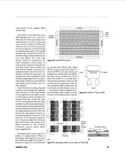
Actel FfGAs. Actel <strong>of</strong>fers three main<br />
<strong>FPGA</strong> families: Act 1, Act 2, a<strong>nd</strong> Act 3.<br />
Although the three generations have<br />
similar features, we focus on the most<br />
recent devices. Unlike the <strong>FPGA</strong>s de-<br />
scribed so far, Actel’s devices use anti-<br />
fuse technology a<strong>nd</strong> a structure similar<br />
to traditional gate arrays. Their design<br />
arranges logic blocks in rows with hor-<br />
izontal routing channels between adja-<br />
cent rows (Figure 25). Actel logic<br />
blocks, based on multiplexers, are<br />
small compared to those based on<br />
lookup tables. Figure 26 illustrates the<br />
Act 3 logic block, which consists <strong>of</strong> an<br />
AND a<strong>nd</strong> an OR gate connected to a<br />
multiplexer-based circuit block. In com-<br />
bination with the two logic gates, the<br />
arrangement <strong>of</strong> the multiplexer circuit<br />
enables a single logic block to realize a<br />
wide range <strong>of</strong> functions. About half the<br />
logic blocks in an Act 3 device also con-<br />
tain a flip-flop.<br />
Actel’s horizontal routing channels<br />
consist <strong>of</strong> various-length wire segments<br />
with antifuses to connect logic blocks<br />
to wire segments or one wire to anoth-<br />
er. Although not shown in Figure 25,<br />
vertical wires also overlie the logic<br />
blocks, forming signal paths that span<br />
multiple rows. The speed performance<br />
<strong>of</strong> Actel chips is not fully predictable be<br />
cause the number <strong>of</strong> antifuses traversed<br />
by a signal depe<strong>nd</strong>s on how CAD tools<br />
allocate the wire segments during cir-<br />
cuit implementation. However, a rich<br />
selection <strong>of</strong> wire segment lengths in<br />
each channel a<strong>nd</strong> algorithms that guar-<br />
antee strict limits on the number <strong>of</strong> an-<br />
tifuses traversed by any two-point<br />
connection improve speed perfor-<br />
mance significantly.<br />
Quicklogic pASZC. Actel’s main com-<br />
petitor in antifuse-based <strong>FPGA</strong>s is<br />
Quicklogic, which has two device fam-<br />
ilies, PASIC a<strong>nd</strong> pASIC2. The pASIC, il-<br />
lustrated in Figure 27a, has similarities<br />
Routing<br />
channels<br />
n<br />
I/O blocks<br />
U U<br />
I I/O blocks<br />
Figure 25. Actel <strong>FPGA</strong> structure.<br />
to several other <strong>FPGA</strong>s: Like Xilinx<br />
<strong>FPGA</strong>s, it has an array-based structure;<br />
like Actel <strong>FPGA</strong>s, its logic blocks use<br />
multiplexers; a<strong>nd</strong> like Altera Flex 8OOOs,<br />
its interconnect consists only <strong>of</strong> long<br />
lines. The pASIC2 is a recently intro-<br />
duced enhanced version, which we will<br />
not discuss here. Cypress also <strong>of</strong>fers de-<br />
vices using the pASlC architecture, but<br />
we discuss only Quicklogic’s version.<br />
Quicklogic’s ViaLink antifuse struc-<br />
ture (see Figure 27b) consists <strong>of</strong> a metal<br />
top layer, an amorphoussilicon insulat-<br />
-0 o~ ... n<br />
U<br />
U<br />
. .<br />
...<br />
...<br />
...<br />
...<br />
...<br />
. .<br />
block<br />
Multiplexer-based<br />
Inputs circuit block * output<br />
Inputs<br />
Figure 26. Actel Act 3 logic module.<br />
-<br />
U<br />
U<br />
0<br />
ViaLink . . at every<br />
: : Loaic cell i i . .<br />
wire<br />
crossing<br />
...<br />
... - - U uu<br />
110 blocks<br />
[a) (b)<br />
Figure 27. Quicklogic pASlC structure (aj a<strong>nd</strong> ViaLink (bj.<br />
SUMMER 1996 55<br />
Metal 1


