

FPGA a:nd CPLD Architectures: A Tutorial - IEEE Design & Test of ...
FPGA a:nd CPLD Architectures: A Tutorial - IEEE Design & Test of ...
FPGA a:nd CPLD Architectures: A Tutorial - IEEE Design & Test of ...

Create successful ePaper yourself
Turn your PDF publications into a flip-book with our unique Google optimized e-Paper software.
all other <strong>CPLD</strong>s: Instead <strong>of</strong> containing<br />
AND/OR logic, a CFB can serve as a<br />
IO-ns SRAM block. Figure 15b shows a<br />
CFB configured as a PAL, a<strong>nd</strong> Figure<br />
15c shows another configured as an<br />
SRAM. In the SRAM configuration, the<br />
PAL block becomes a 128-word by 10-<br />
bit read/write memory. Inputs that<br />
would normally feed the AND plane in<br />
the PAL become address lines, data<br />
lines, or control signals for the memo-<br />
ry. Flip-flops a<strong>nd</strong> tristate buffers are still<br />
available in the SRAM configuration.<br />
In the Flashlogic device, the AND/OR<br />
logic plane's configuration bits are<br />
SRAM cells connected to EPROM or<br />
EEPROM cells. Applying power loads<br />
the SRAM cells with a copy <strong>of</strong> the non-<br />
volatile EPROM or EEPROM, but the<br />
SRAM cells control the chip's configu-<br />
ration. The user can reconfigure the<br />
chips in system by downloading new in-<br />
formation into the SRAM cells. The user<br />
can make the SRAM cell reprogram-<br />
ming nonvolatile by writing the SRAM<br />
cell contents back to the EPROM cells.<br />
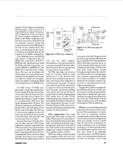
ICT PEEL Arrays. ICT PEEL (pro-<br />
grammable, electrically-erasable logic)<br />
Arrays are large PLAs that include logic<br />
macrocells with flop-flops a<strong>nd</strong> feed-<br />
back to the logic planes. Figure 16 il-<br />
lustrates this structure, which consists<br />
<strong>of</strong> a programmable AND plane that<br />
feeds a programmable OR plane. The<br />
OR plane's outputs are partitioned into<br />
groups <strong>of</strong> four, a<strong>nd</strong> each group can be<br />
input to any <strong>of</strong> the logic cells. The log-<br />
ic cells provide registers for the sum<br />
terms a<strong>nd</strong> can feed back the sum terms<br />
to the AND plane. Also, the logic cells<br />
connect sum terms to I/O pins.<br />
Because they have a PLA-like struc-<br />
ture, the logic capacity <strong>of</strong> PEEL Arrays<br />
is difficult to measure compared to the<br />
<strong>CPLD</strong>s discussed so far, but we estimate<br />
a capacity <strong>of</strong> 1,600 to 2,800 equivalent<br />
gates. Containing relatively few I/O pins,<br />
the largest PEEL Array comes in a 40-pin<br />
package. Since they do not consist <strong>of</strong><br />
SPLD-like blocks, PEEL Arrays do not fit<br />
SUMMER 1996<br />
El-<br />
Input<br />
pins<br />
terms<br />
I/O<br />
&<br />
pins<br />
U<br />
'Group <strong>of</strong> four<br />
sum terms<br />
Figure 76. ICT PEEL Array architecture<br />
well into the <strong>CPLD</strong> category.<br />
Nevertheless, we include them here be<br />
cause they exemplify PLA-based (rather<br />
than PAL-based) devices a<strong>nd</strong> <strong>of</strong>fer larg-<br />
er capacity than a typical SPLD.<br />
The PEEL Array logic cell, shown in<br />
Figure 17, includes a flip-flop, config-<br />
urable as D, T, or JK, a<strong>nd</strong> two multi-<br />
plexers. Each multiplexer produces a<br />
logic cell output, either registered or<br />
combinational. One logic cell output<br />
can connect to an I/O pin, a<strong>nd</strong> the oth-<br />
er output is buried. An interesting fea-<br />
ture <strong>of</strong> the logic cell is that the flip-flop<br />
clock, preset, a<strong>nd</strong> clear are full sum-<strong>of</strong>-<br />
product logic functions. Distinguishing<br />
PEEL Arrays from all other <strong>CPLD</strong>s,<br />
which simply provide product terms for<br />
these signals, this feature is attractive for<br />
some applications. Because <strong>of</strong> their<br />
PLA-like OR plane, PEEL Arrays are es-<br />
pecially well suited to applications that<br />
require very wide sum terms.<br />
<strong>CPLD</strong> applications. Their high<br />
speeds a<strong>nd</strong> wide range <strong>of</strong> capacities<br />
make <strong>CPLD</strong>s useful for many applications,<br />
from implementing ra<strong>nd</strong>om glue<br />
logic to prototyping small gate arrays.<br />
An important reason for the growth <strong>of</strong><br />
the <strong>CPLD</strong> market is the conversion <strong>of</strong><br />
designs that consist <strong>of</strong> multiple SPLDs<br />
into a smaller number <strong>of</strong> <strong>CPLD</strong>s.<br />
<strong>CPLD</strong>s can realize complex designs<br />
such as graphics, LAN, a<strong>nd</strong> cache controllers.<br />
As a rule <strong>of</strong> thumb, circuits that<br />
Four<br />
sum A+.-$-<br />
erms<br />
I Global reset<br />
Figure 77. ICJ PEEL Array logic cell<br />
structure.<br />
:an exploit wide AND/OR gates a<strong>nd</strong> do<br />
iot need a large number <strong>of</strong> flip-flops are<br />
good ca<strong>nd</strong>idates for <strong>CPLD</strong> implemen-<br />
ation. Finite state machines are an ex-<br />
:ellent example <strong>of</strong> this class <strong>of</strong> circuits.<br />
4 significant advantage <strong>of</strong> <strong>CPLD</strong>s is that<br />
hey allow simple design changes<br />
hrough reprogramming (all commer-<br />
5al <strong>CPLD</strong> products are reprogramma-<br />
de). In-system programmable <strong>CPLD</strong>s<br />
?veri make it possible to reconfigure<br />
iardware (for example, change a pro-<br />
ocol for a communications circuit)<br />
Nithout powering down.<br />
<strong>Design</strong>s <strong>of</strong>ten partition naturally into<br />
he SPLD-like blocks in a <strong>CPLD</strong>, pro-<br />
jucing more predictable speed perfor-<br />
nance than a design split into many<br />
small pieces mapped into different ar-<br />
?as <strong>of</strong> the chip. Predictability <strong>of</strong> circuit<br />
mplementation is one <strong>of</strong> the strongest<br />
idvantages <strong>of</strong> <strong>CPLD</strong> architectures.<br />
<strong>FPGA</strong>s. As one <strong>of</strong> the fastest growing<br />
segments <strong>of</strong> the semico<strong>nd</strong>uctor i<strong>nd</strong>us-<br />
ry, the <strong>FPGA</strong> marketplace is volatile.<br />
rhe pool <strong>of</strong> companies involved<br />
Zhanges rapidly, a<strong>nd</strong> it is difficult to say<br />
Nhich products will be most significant<br />
Nhen the i<strong>nd</strong>ustry reaches a stable<br />
state. We focus here on products cur-<br />
cently in widespread use. In describing<br />
2ach device, we list its capacity in two-<br />
nput NAND gates as given by the ven-<br />
joy. Gate count is an especially<br />
zontentious issue in the <strong>FPGA</strong> i<strong>nd</strong>ustry,<br />
md so the numbers given should not<br />
3e taken too seriously. In fact, wags<br />
51


