

Alexander (Sandy) Marquardt, Vaughn Betz, and Jonathan Rose
Alexander (Sandy) Marquardt, Vaughn Betz, and Jonathan Rose
Alexander (Sandy) Marquardt, Vaughn Betz, and Jonathan Rose

Create successful ePaper yourself
Turn your PDF publications into a flip-book with our unique Google optimized e-Paper software.
ABSTRACT<br />
SPEED AND AREA TRADE-OFFS IN CLUSTER-BASED FPGA ARCHITECTURES<br />
One way to reduce the delay <strong>and</strong> area of FPGAs is to employ logiccluster-based<br />
architectures, where a logic cluster is a group of logic<br />
elements connected with high-speed local interconnections. In this<br />
paper we empirically evaluate FPGA architectures with logic clusters<br />
ranging in size from 1 to 20, <strong>and</strong> show that compared to architectures<br />
with size 1 clusters, architectures with size 8 clusters have<br />
23% less delay (30% faster clock speed), <strong>and</strong> require 14% less<br />
area. We also show that FPGA architectures with large cluster sizes<br />
can significantly reduce design compile time — an increasingly<br />
important concern as the logic capacity of FPGAs rises. For example,<br />
an architecture that uses size 20 clusters requires 7 times less<br />
compile time than an architecture with size 1 clusters.<br />
INDEX TERMS<br />
<strong>Alex<strong>and</strong>er</strong> (<strong>S<strong>and</strong>y</strong>) <strong>Marquardt</strong>, <strong>Vaughn</strong> <strong>Betz</strong>, <strong>and</strong> <strong>Jonathan</strong> <strong>Rose</strong><br />
Clustering, design, gate-array, high-speed-interconnect, performance-trade-offs,<br />
high-performance.<br />
1. INTRODUCTION<br />
Field-Programmable Gate Arrays (FPGAs) have become one of the<br />
most popular implementation media for digital circuits, <strong>and</strong> since<br />
their introduction in 1984 FPGAs have become a multi-billion<br />
dollar industry. The key to the success of FPGAs is their programmability,<br />
which allows any circuit to be instantly realized by appropriately<br />
programming an FPGA.<br />
FPGAs have some compelling advantages over St<strong>and</strong>ard Cells or<br />
Mask-Programmed Gate Arrays (MPGAs): faster time-to-market,<br />
lower non-recurring engineering costs (NRE), <strong>and</strong> easier debugging.<br />
Additionally, FPGAs offer designers the ability to fix errors<br />
or to add features to systems that have already been manufactured.<br />
FPGAs are also useful for implementing designs that are low<br />
volume or are required immediately, since they do not require<br />
design specific manufacturing like St<strong>and</strong>ard Cells or MPGAs.<br />
The benefits offered by FPGAs come at a price — FPGAs are at<br />
least three times slower, <strong>and</strong> require at least ten times the area of<br />
MPGAs [1]. This loss in speed is mainly due to the fact that logic<br />
in FPGAs is connected via programmable switches, while in St<strong>and</strong>ard<br />
Cells or MPGAs, logic is connected with metal wires. The<br />
programmable switches in FPGAs have high resistance <strong>and</strong> capacitance<br />
compared to the metal wiring in St<strong>and</strong>ard Cells or MPGAs,<br />
<strong>and</strong> therefore reduce circuit speed. Interconnect delay is more significant<br />
(typically well over 50% of the total circuit delay) in<br />
FPGAs than it is in MPGAs or St<strong>and</strong>ard Cells, <strong>and</strong> consequently it<br />
is more important to minimize the interconnect delay in FPGAs<br />
than it is in MPGAs or St<strong>and</strong>ard Cells.<br />
Another important factor affecting circuit delay is the process used<br />
in the manufacture of an FPGA. As process geometries shrink into<br />
the deep-submicron region, interconnect resistance <strong>and</strong> capacitance<br />
become increasingly significant — smaller processes which result<br />
Right Track CAD Corp.<br />
#313 - 720 Spadina Ave.<br />
Toronto, ON, Canada M5S 2T9<br />
{arm, vaughn, jayar}@rtrack.com<br />
in improvements in logic speed do not result in similar improvements<br />
in interconnect speed. The result of this is that as processes<br />
shrink, interconnect delay accounts for an increasing proportion of<br />
total circuit delay. Clearly, interconnect delay must be minimized<br />
in order to achieve the best possible circuit performance.<br />
The design of an FPGA’s architecture can have a significant impact<br />
on the performance of circuits implemented in the FPGA. In this<br />
work we explore FPGA architectures composed of logic clusters,<br />
where a logic cluster is a grouping of logic elements connected<br />
with high-speed local interconnections. Altera’s FLEX 6K, 8K <strong>and</strong><br />
10K [2], the Xilinx 5200 <strong>and</strong> Virtex [3][4], the newest Actel [5],<br />
<strong>and</strong> the Vantis VF1 [6] parts all employ some form of cluster-based<br />
logic blocks, so research in this area is of clear commercial relevance.<br />
It is also of interest to see how cluster size affects design compile<br />
time. An FPGA composed of large clusters requires fewer logic<br />
blocks to implement a circuit than an FPGA using small clusters.<br />
This reduces the size of the placement <strong>and</strong> routing problem, <strong>and</strong><br />
hence reduces design compile time.<br />
Previous work on logic-cluster based architectures considered only<br />
area [7][8]. An earlier version of this work considered circuit speed<br />
[10] but used a CAD flow that was not completely timing-driven.<br />
In this work we make use of a completely timing-driven CAD flow<br />
(including a new timing-driven placement algorithm) to evaluate<br />
the effect of cluster size on FPGA speed <strong>and</strong> area.<br />
This paper is organized as follows. Section 2 introduces the structure<br />
of cluster-based logic blocks. In Section 3 we outline the<br />
experimental methodology used to evaluate the utility of different<br />
cluster sizes. Section 4 discusses how area <strong>and</strong> delay are modeled.<br />
Section 5 discusses the area-delay product metric, <strong>and</strong> why we<br />
believe it is a useful tool for comparing different architectures.<br />
Section 6 describes how we selected various parameters for the different<br />
cluster sizes. Section 7 presents area <strong>and</strong> delay results for<br />
various cluster sizes, while Section 8 shows how design compile<br />
time is affected by different cluster sizes. Section 9 discuses potential<br />
sources of inaccuracies. Finally, in Section 10 we present our<br />
conclusions.<br />
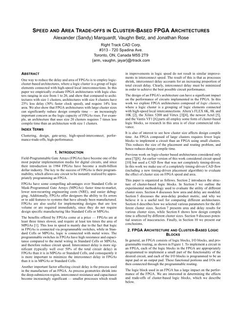
2. FPGA ARCHITECTURE AND CLUSTER-BASED LOGIC<br />
BLOCKS<br />
In general, an FPGA consists of logic blocks, I/O blocks, <strong>and</strong> programmable<br />
routing, as shown in Figure 1. To implement a circuit in<br />
an FPGA, each of the logic blocks in the FPGA are appropriately<br />
programmed to implement a small part of the functionality of the<br />
desired circuit, <strong>and</strong> each of the I/O blocks is programmed to be an<br />
input pad or an output pad. These functional portions <strong>and</strong> I/Os are<br />
then connected through the programmable routing.<br />
The logic block used in an FPGA has a large impact on the performance<br />
of the FPGA. We are interested in determining the effects<br />
<strong>and</strong> trade-offs of cluster-based logic blocks, which we describe<br />
below.
Logic<br />
Programmable<br />
block routing<br />
I/O block<br />
Figure 1 A generic FPGA [1]<br />
2.1 CLUSTER-BASED LOGIC BLOCKS<br />
We are interested in studying logic blocks which consist of a<br />
grouping of basic logic elements (BLEs) connected with fast local<br />
interconnect. In general, a BLE is a small indivisible unit combining<br />
sequential <strong>and</strong> combinational logic; the BLE that we study consists<br />
of a 4-LUT <strong>and</strong> a flip-flop as shown in Figure 2-a. A logic<br />
block combining one 1 or more BLEs is known as a logic cluster<br />
[8][9]. Figure 2-b shows the structure of a logic cluster consisting<br />
of N BLEs <strong>and</strong> the routing required to connect them together.<br />
The clusters that we study are fully-connected, meaning that any<br />
BLE input can connect to any cluster input or any BLE output.<br />
Since the cluster is fully connected it is possible to bring a net into<br />
the cluster on a single cluster input, <strong>and</strong> route this net to many<br />
BLEs within the cluster via the local routing. This allows the<br />
number of nets brought into the cluster (number of cluster inputs<br />
used) to be less than the total number of BLE inputs within the<br />
cluster. Another benefit of fully connected clusters is that CAD<br />
tools are simplified since all BLEs within the cluster are logically<br />
equivalent.<br />
A logic cluster consisting of BLEs is described with the following<br />
four parameters [8][9]:<br />
1. The size of (number of inputs to) a LUT (K),<br />
2. Cluster size (N) — the number of BLEs in a cluster,<br />
3. The number of inputs to the cluster for use as inputs by the<br />
LUTs (I), <strong>and</strong><br />
4. The number of clock inputs to a cluster (for use by the<br />
registers), Mclk.<br />
This work focuses on logic clusters in which the LUT size, K, is 4<br />
<strong>and</strong> the number of clock pins on a cluster, M clk , is 1 — this is the<br />
case shown in Figure 2, <strong>and</strong> was also the case used in [8][9], <strong>and</strong><br />
[10]. Note that the total number of BLE inputs is K·N; however,<br />
only I inputs are brought into the cluster.<br />
1 A logic cluster that consists of only one BLE has no local routing.<br />
Inputs<br />
Clock<br />
I<br />
Inputs<br />
Clock<br />
I<br />
[7] [8] showed that FPGAs composed of logic clusters of size 1-10<br />
BLEs have the best area efficiency. That research did not consider<br />
the effect of cluster size on circuit speed, however, it did speculate<br />
that larger cluster sizes would have a positive impact on FPGA performance.<br />
3. EXPERIMENTAL METHODOLOGY<br />
We use an empirical method to explore different FPGA architectures.<br />
This involves technology-mapping, packing, placing, <strong>and</strong><br />
routing benchmark circuits 2 into realistic architectures with clusters<br />
of size 1 through 20. The area <strong>and</strong> delay of each circuit implementation<br />
is then computed using sophisticated models, <strong>and</strong> we are<br />
able to judge the quality of each architecture.<br />
3.1 CAD FLOW<br />
(a) Basic Logic Element (BLE)<br />
4-<br />
LUT<br />
Local<br />
Routing<br />
(X-Bar)<br />
DFF<br />
BLE<br />
#1<br />
. . .<br />
BLE<br />
#N<br />
(b) Logic Cluster<br />
Out<br />
Outs<br />
Figure 2 Logic cluster <strong>and</strong> basic logic element (BLE)<br />
The CAD flow that we use to evaluate different FPGA architectures<br />
is basically the same as in [8][9], <strong>and</strong> is given in Figure 3.<br />
First each circuit is logic-optimized by SIS [12] <strong>and</strong> technology<br />
mapped into 4-LUTs by FlowMap [13]. Then the timing-driven<br />
packing algorithm, T-VPack [10][14] is used to group the LUTs<br />
<strong>and</strong> registers into logic clusters of the desired size with the desired<br />
number of inputs. After this each circuit is mapped onto an FPGA<br />
by a timing-driven placement tool called T-VPlace [14] that we<br />
2 Our benchmarks consist of the 20 largest MCNC circuits [11].<br />
The circuits range in size from 1047 to 8383 4-LUTs. The circuits<br />
used are: alu4, apex2, apex4, bigkey, clma, des, diffeq, dsip, elliptic,<br />
ex1010, ex5p, frisc, misex3, pdc, s298, s38417, s38584.1, seq,<br />
spla, <strong>and</strong> tseng.<br />
N
Circuit<br />
Logic optimization (SIS)<br />
Technology map to 4-LUTS (FlowMap + Flowpack)<br />
Cluster<br />
Parameters<br />
(N, I, K)<br />
Routing<br />
Architecture<br />
Parameters<br />
(Fc, etc.)<br />
Pack FFs <strong>and</strong> LUTs into<br />
logic clusters (T-VPack)<br />
Placement (VPR,<br />
T-VPlace)<br />
Routing (VPR,<br />
timing-driven router)<br />
Min #<br />
tracks?<br />
Adjust channel<br />
capacities (W)<br />
Figure 3 Architecture evaluation CAD flow [8][9].<br />
have incorporated into VPR. Finally, VPR’s timing-driven router is<br />
used to connect all of the wiring.<br />
T-VPack [10][14] is a timing-driven version of the VPack algorithm<br />
developed in [8]. The T-VPack algorithm takes a netlist of<br />
LUTs <strong>and</strong> registers (BLEs), <strong>and</strong> produces a netlist of logic clusters<br />
as shown in Figure 4. T-VPack maps BLEs into clusters so that<br />
physical constraints on the number of inputs (I), number of BLEs<br />
(N), <strong>and</strong> the number of clocks (Mclk) are satisfied. In addition to<br />
meeting physical constraints, T-VPack has two optimization goals<br />
1. To minimize the number of cluster inputs used, which<br />
minimizes the number of point-to-point connections in the<br />
post-clustering circuit.<br />
2. To pack BLEs along the critical path into as few clusters as<br />
possible so that many critical connections use the fast routing<br />
inside the logic clusters.<br />
After packing is complete, the next stage in the CAD flow is placement<br />
which is done with T-VPlace [14]. The T-VPlace algorithm is<br />
an extension to the VPlace algorithm developed in [8][9]. It is<br />
given a netlist of circuit blocks (I/Os or logic clusters), <strong>and</strong> maps<br />
each circuit block into a physical location in the FPGA. This algorithm<br />
is simulated annealing [15][16][17] based <strong>and</strong> optimizes the<br />
No<br />
Yes - Wmin determined<br />
Routing with W = 1.35 Wmin<br />
(VPR, timing-driven router)<br />
Determine critical path delay <strong>and</strong><br />
transistor area to build FPGA<br />
(VPR + TransCount)<br />
Netlist of BLEs<br />
final placement to minimize the required routing area as well as<br />
minimizing the critical path delay.<br />
The next stage in the CAD flow is routing. The router in VPR [8]<br />
[9] is fully timing-driven <strong>and</strong> attempts to minimize the critical path<br />
delay (given the current placement).<br />
Figure 3 shows how VPR computes the minimum number of tracks<br />
in which a circuit will route, which we refer to as a high-stress<br />
routing. Basically VPR repeatedly routes each circuit with different<br />
channel widths (number of tracks per channel), scaling the FPGA’s<br />
architecture until it finds the minimum number of tracks in which<br />
the circuit will route. We define a low-stress routing to occur when<br />
an FPGA has 35% more routing resources than the minimum<br />
required to route a given circuit. We feel that low-stress routings<br />
are indicative of how an FPGA will generally be used (it is rare that<br />
a user will utilize 100% of all routing <strong>and</strong> logic resources), so our<br />
delay results are based on low-stress routings.<br />
By allowing the channel width to vary, <strong>and</strong> searching for the minimum<br />
routable width, we can detect small improvements in FPGA<br />
architectures or CAD algorithms that might otherwise go unnoticed.<br />
Compare this to mapping a circuit into a fixed size FPGA —<br />
this would only tell us if the circuit fit or not. A “binary” result like<br />
this makes it is difficult to draw conclusions about new architectures.<br />
After placement <strong>and</strong> routing, we know exactly how each benchmark<br />
circuit is embedded into the FPGA architecture under consideration.<br />
This allows us to apply the detailed area <strong>and</strong> delay models<br />
described in Section 4 to evaluate the area <strong>and</strong> delay of each implementation.<br />
4. ARCHITECTURE MODELING<br />
In this section we first describe the area <strong>and</strong> delay models that we<br />
use to evaluate the various FPGA architectures. After this we<br />
describe the effect that varying cluster size has on segment lengths,<br />
<strong>and</strong> transistor sizing.<br />
4.1 AREA MODEL<br />
A<br />
B<br />
F G C H<br />
D<br />
E<br />
BLEs<br />
Pack<br />
Netlist of Clusters<br />
Clusters<br />
Figure 4 Packing example<br />
A B<br />
C D<br />
F G<br />
E H<br />
The area model 1 that we use is based on counting the number of<br />
minimum-width transistor areas required to implement each FPGA<br />
architecture, which is the same model as was used in [8][9]. A minimum-width<br />
transistor area is simply the layout area occupied by<br />
the smallest transistor that can be contacted in a process, plus the<br />
1 Note that the area model is based on transistor-area rather than<br />
metal area, since transistor area determines the die size of current<br />
FPGAs.
Routing Segment<br />
A B C<br />
....<br />
Fc<br />
{<br />
Input<br />
Connection<br />
Buffers<br />
& Muxes<br />
{ ....<br />
....<br />
minimum spacing to another transistor above it <strong>and</strong> to its right [8].<br />
By counting the number of minimum-width transistor areas<br />
required to implement an FPGA, rather than the number of square<br />
microns which these transistors would occupy, we obtain a process-independent<br />
estimate of the FPGA area. The area model that<br />
we use is described in detail in [8][9].<br />
We use a program called TransCount [9], to determine the area of a<br />
cluster-based logic block (including the local cluster routing) with<br />
any values of N, I, K, <strong>and</strong> M clk . This program models such effects<br />
as buffer resizing as a function of the fanout of the connections<br />
within a logic block, <strong>and</strong> builds multi-stage buffers when high<br />
drive strengths are required. Since the area of an FPGA includes<br />
both logic block area <strong>and</strong> routing area, we use VPR to determine<br />
the transistor-count of the area taken by the routing for each FPGA<br />
of interest, <strong>and</strong> by adding this area to the logic block area we obtain<br />
the total FPGA area.<br />
4.2 DELAY MODEL<br />
Local<br />
Buffers<br />
Local<br />
Routing<br />
Muxes<br />
{<br />
4<br />
LUT<br />
....<br />
Logic Cluster<br />
BLE<br />
The delays of the connections within logic clusters were found by<br />
performing SPICE simulations using TSMC’s 0.35 μm process for<br />
each structure in the cluster. Figure 5 shows the major structures<br />
<strong>and</strong> speed paths in a logic cluster. Important delay values through<br />
this cluster are shown in Table 1, however some delays cannot be<br />
listed because the process information is proprietary <strong>and</strong> was<br />
obtained under a non-disclosure agreement.<br />
VPR has a built-in delay estimator that uses a modified Elmore<br />
delay [18] model to estimate the delay of each connection in the<br />
routing. The modifications to the Elmore delay are described in<br />
[19], <strong>and</strong> are such that it can be used to estimate delay of circuits<br />
containing buffers, resistors, <strong>and</strong> capacitors. After every connection’s<br />
delay in the circuit has been computed, VPR performs a<br />
path-based timing analysis using these inter-cluster connection<br />
delay values (Elmore delay) <strong>and</strong> intra-cluster delay values<br />
(Table 1). A full description of the timing analyzer used in VPR is<br />
available in [8] or [9].<br />
4.3 EFFECT OF CLUSTER SIZE ON THE PHYSICAL LENGTH OF<br />
FPGA ROUTING SEGMENTS<br />
As we increase the cluster size, both the logic area per cluster <strong>and</strong><br />
routing area per cluster grow. Figure 6 demonstrates how a tile (a<br />
logic block plus its associated routing) grows as cluster size is<br />
increased. This increased tile size results in routing segments with<br />
FF<br />
N<br />
BLEs<br />
D<br />
Figure 5 Detailed Logic Cluster Structure<br />
Routing Segment<br />
Table 1: Intra-cluster delays in TSMC’s 0.35 μm CMOS<br />
process (letters correspond to points labelled in<br />
Figure 5).<br />
Cluster<br />
Size (N)<br />
1 (No local<br />
routing<br />
muxes)<br />
A to B<br />
(ps)<br />
B to C<br />
<strong>and</strong> D to<br />
C (ps)<br />
760 140 (<strong>and</strong><br />
no D to C<br />
path)<br />
C to D<br />
(ps)<br />
B to D<br />
(ps)<br />
379 519<br />
2 760 687 379 1066<br />
4 760 761 379 1140<br />
8 760 902 379 1281<br />
16 760 1054 379 1433<br />
20 760 1081 379 1460<br />
the same “logical length” having different physical lengths for<br />
logic clusters of different sizes, where the logical length of a routing<br />
segment is the number of logic blocks that the segment spans.<br />
We call the measured length of a routing segment its physical<br />
length. The resistance <strong>and</strong> capacitance of a routing segment grow<br />
linearly with the segment’s physical length. We have experimentally<br />
determined the average rate at which the FPGA tiles grow<br />
with cluster size, <strong>and</strong> have used this information to appropriately<br />
scale the routing segment resistance <strong>and</strong> capacitance values for the<br />
various cluster sizes. The increase in the resistance <strong>and</strong> capacitance<br />
of routing segments as the size of the FPGA logic block increases<br />
is an important effect that has often been neglected in prior FPGA<br />
architecture research.<br />
4.4 SIZING ROUTING TRANSISTORS TO COMPENSATE FOR<br />
DIFFERENT PHYSICAL SEGMENT LENGTHS<br />
To compensate for differences in the capacitance <strong>and</strong> resistance of<br />
routing segments in FPGAs using different sizes of logic clusters,<br />
we scale the routing pass transistors <strong>and</strong> buffers. All of our pass<br />
transistor <strong>and</strong> buffer scaling is in relation to a base architecture that<br />
has been area-delay optimized for clusters of size four. From this<br />
base architecture, we linearly scale routing buffers <strong>and</strong> pass transistors<br />
depending on the relation between the new segment lengths<br />
<strong>and</strong> the base segment length. For example, in an FPGA with size<br />
Channel<br />
width<br />
{<br />
Logic<br />
cluster<br />
Segment length<br />
Increase<br />
cluster<br />
size<br />
Increased<br />
channel<br />
width<br />
{<br />
Increased<br />
logic<br />
area<br />
per cluster<br />
Logic<br />
cluster<br />
Increased<br />
routing<br />
area<br />
per cluster<br />
Increased segment length<br />
Figure 6 Effect of cluster size on physical length of routing
16 clusters, the physical segment length is approximately 2 times<br />
longer than in an architecture with size 4 clusters. To maintain<br />
roughly the same speed per routing segment, we increase the size<br />
of the routing switches connecting to each wire by a factor of 2. In<br />
Section 7.4 we verify that this linear scaling of buffers <strong>and</strong> passtransistors<br />
with physical segment length provides good results.<br />
VPR models the changes in delay caused by resizing buffers <strong>and</strong><br />
pass-transistors in the routing, <strong>and</strong> it also accurately models the<br />
area required for different sizes of routing pass-transistors <strong>and</strong><br />
buffers.<br />
5. ARCHITECTURE EVALUATION — AREA-DELAY<br />
PRODUCT<br />
One metric that we will use to evaluate the quality of different<br />
architectures is the area-delay product. We feel that there are two<br />
reasons that this metric makes sense:<br />
1. Intuitively, we want to find the point at which we are<br />
sacrificing the least amount of area for the most improvement<br />
in speed. Given that we can always trade area for speed (see<br />
below), <strong>and</strong> speed for area, it makes sense to combine these<br />
two factors into one curve to see where the best trade-off<br />
occurs.<br />
2. Much of the performance gain from using an FPGA is derived<br />
from parallelizing functional units, rather than raw clock<br />
speed. In this case, throughput = number of functional units ⋅<br />
clock rate. Another way of looking at this is, throughput = (1/<br />
area per functional unit) ⋅ (1/delay). Therefore if we minimize<br />
the area-delay product, we will maximize throughput.<br />
There are two main factors which can affect the area-delay product<br />
of an FPGA: transistor sizing, <strong>and</strong> the FPGA architecture. In general,<br />
the speed of an FPGA can be increased (to a point) by sizing<br />
up the buffers <strong>and</strong> transistors within the FPGA, but this increases<br />
area. Alternatively, the FPGA can be made smaller by sizing down<br />
the buffers <strong>and</strong> transistors, but this degrades the FPGA performance.<br />
Throughout this paper, we will size the transistors in each FPGA<br />
architecture to minimize the FPGA’s area-delay product. Only by<br />
resizing transistors appropriately for each architecture in this way<br />
can we fairly compute the speed <strong>and</strong> area-efficiency of FPGAs<br />
with different logic block architectures.<br />
6. ARCHITECTURE PARAMETERS<br />
To evaluate the speed <strong>and</strong> area of an FPGA employing logic clusters<br />
for its logic blocks, we must choose not only the logic block<br />
architecture <strong>and</strong> transistor sizes, but also a routing architecture <strong>and</strong><br />
the flexibility of the logic block to routing interface. The following<br />
sections detail the architectural parameters used in our experiments.<br />
6.1 BASIC ARCHITECTURE<br />
We investigate isl<strong>and</strong>-style FPGAs in which each logic cluster is<br />
surrounded by routing channels on all four sides with the logic<br />
cluster input <strong>and</strong> output pins evenly distributed around the logic<br />
cluster perimeter. This basic architecture was shown in Figure 1.<br />
For our experiments each circuit is mapped to the smallest square<br />
FPGA with enough logic clusters <strong>and</strong> I/O pads to accommodate it.<br />
In our experiments, we vary the number of I/O pads per row or<br />
column depending on the cluster size. Since a large cluster size<br />
requires fewer clusters to implement a given circuit, we require<br />
more I/O pads per row or column. We set the number of I/O pads<br />
per row or column to<br />
Pads = 2 ⋅ Cluster_Size<br />
(1.1)<br />
Setting the number of I/O pads per row or column with the above<br />
equation keeps the total number of I/O pads roughly the same for<br />
each FPGA architecture, independent of the cluster size that is<br />
used.<br />
Recall that we describe a logic cluster with four parameters: the<br />
number of logic inputs (I), the number of BLEs (LUTs <strong>and</strong> registers)<br />
in a cluster (N), the number of clock inputs (M clk ), <strong>and</strong> the<br />
number of inputs to each LUT (K). We fix the number of clocks per<br />
cluster at one for all our experiments, since the MCNC benchmark<br />
circuits we use to evaluate architectures all have only one clock.<br />
We set the number of inputs to each LUT, K, to 4, since previous<br />
research has shown LUTs of this size are the most area-efficient<br />
[20], <strong>and</strong> because this is the LUT size used in most commercial<br />
FPGAs. We describe how we set the number of inputs, I, in the<br />
next section.<br />
6.2 INPUTS REQUIRED VS. CLUSTER SIZE<br />
Previous work [8] has examined the issue of how many cluster<br />
inputs are required for 98% utilization of the logic clusters, where<br />
utilization is defined as<br />
num logic blocks<br />
---------------------------------------------cluster<br />
size<br />
utilization =<br />
-----------------------------------------------------num<br />
clusters used<br />
(1.2)<br />
That research, however, used VPack to map logic into the clusters.<br />
Since we are using our new T-VPack algorithm for packing in our<br />
cluster-based logic block experiments, <strong>and</strong> because T-VPack has<br />
better utilization than VPack, it is prudent to re-run these experiments<br />
with T-VPack. Figure 7 shows the number of inputs required<br />
to achieve an average utilization of 98% vs. cluster size for both<br />
VPack <strong>and</strong> T-VPack 1 . We use the T-VPack results of this experiment<br />
to set the number of physical inputs per cluster for the<br />
remainder of our architecture studies.<br />
6.3 ROUTING ARCHITECTURE<br />
Recall that we define the number of logic blocks which a routing<br />
segment spans as the logical length of that segment. In [8][9] it is<br />
shown that an architecture in which routing segments have a logical<br />
length of four, with 50% of the segments connected by tri-state<br />
buffers <strong>and</strong> 50% connected by pass-transistors, provides good areaefficiency<br />
<strong>and</strong> speed for FPGAs containing logic clusters of size<br />
four. This routing architecture is shown in Figure 8. We implicitly<br />
assume that this routing architecture is good for architectures containing<br />
logic clusters of all sizes, <strong>and</strong> we use this routing architecture<br />
in all of our experiments. Ideally, one would find the best<br />
routing architecture for each FPGA employing a different cluster<br />
size, but this would require a huge amount of effort. By basing all<br />
of our experiments on this routing architecture, we may slightly<br />
favor architectures with size four clusters over other architectures.<br />
1 This shows that T-VPack reduces the number of inputs required<br />
vs. T-VPack for 98% utilization at large cluster sizes. The fact that<br />
the two tools have different requirements for the number of inputs<br />
is an example of the dependencies between FPGA architecture<br />
<strong>and</strong> CAD.
Number of Cluster Inputs (I)<br />
(20 Benchmark Average)<br />
45<br />
40<br />
35<br />
30<br />
25<br />
20<br />
15<br />
10<br />
5<br />
T-Vpack<br />
Vpack<br />
0<br />
0 2 4 6 8 10 12 14 16 18 20<br />
Figure 7 Inputs required for 98% utilization vs. cluster size<br />
6.4 FLEXIBILITY OF LOGIC BLOCK TO ROUTING<br />
INTERCONNECT VS. CLUSTER SIZE<br />
For a cluster of size 1 [21] showed that a good value of F c (the<br />
number of routing tracks to which each logic block pin can connect)<br />
is W (the total number of tracks in a channel); This value of<br />
F c means that each logic block pin can connect to any routing track<br />
in an adjacent channel. However, for large clusters, setting F c to W<br />
provides far more routing flexibility than is required, wasting area.<br />
[8] found that a more appropriate level of routing flexibility results<br />
when the F c value for logic block output pins, F c,output is set to W/<br />
N, so all the experiments in the next section use this value. This<br />
choice of F c,output ensures that all the routing tracks in each channel<br />
can be driven by at least one output from each cluster.<br />
Choosing the appropriate value for F c,input involves finding the<br />
best trade-off between track width <strong>and</strong> area per track as follows<br />
Logic<br />
cluster<br />
Logic<br />
cluster<br />
Logic<br />
cluster<br />
Logic<br />
cluster<br />
Cluster Size (N)<br />
Logic<br />
cluster<br />
Logic<br />
cluster<br />
Logic<br />
cluster<br />
Logic<br />
cluster<br />
Logic<br />
cluster<br />
Logic<br />
cluster<br />
Figure 8 FPGA with length 4 segments, 50% buffered <strong>and</strong> 50%<br />
pass transistor switches.<br />
1. As F c,input is increased, fewer tracks are required to<br />
implement a given circuit since the router has more choices of<br />
which track each input can connect to.<br />
2. Each track takes more area as F c,input is increased since there<br />
are more switches on each track (recall that routing area is<br />
determined by transistor area, not wiring area [8][9]).<br />
Therefore, we must determine the point at which the best trade-off<br />
occurs. We have run experiments on size 4, 8, 14, <strong>and</strong> 20 clusters to<br />
determine the best F c,input values as shown in Table 2, <strong>and</strong> have<br />
linearly interpolated between these results for other cluster sizes.<br />
Table 2: Routing area vs. F c, input for various cluster<br />
F c, input<br />
sizes a<br />
Routing Area for various cluster sizes<br />
(in millions of minimum-width transistors)<br />
4 8 14 20<br />
0.1·W — — — 1.51<br />
0.2·W — — 1.38 1.41<br />
0.3·W — 1.29 1.34 1.41<br />
0.4·W 1.47 1.27 1.34 1.42<br />
0.5·W 1.45 1.28 1.37 1.46<br />
0.6·W 1.44 1.30 — —<br />
0.7·W 1.45 — — —<br />
0.8·W 1.49 — — —<br />
0.9·W 1.50 — — —<br />
Best<br />
F c,input<br />
value<br />
0.6·W 0.4·W 0.3·W 0.2·W<br />
a.The MCNC circuits used for these experiments are the 10 smallest<br />
of the 20 benchmark circuits that we use in all of our other<br />
experiments.<br />
Note, for these experiments, we have noticed that the critical path<br />
is not affected by the F c,,input values chosen, so we choose the<br />
F c,input value based only on the area results.<br />
7. EXPERIMENTAL RESULTS: AREA AND DELAY AT<br />
VARIOUS CLUSTER SIZES<br />
Recall that our goal in this work is to determine the effect of cluster<br />
size on the area <strong>and</strong> speed of FPGAs that use a cluster-based architecture.<br />
The CAD flow of Figure 3 is used to obtain area <strong>and</strong> critical-path<br />
delay estimations for the 20 benchmark circuits<br />
implemented in architectures with clusters of size one through<br />
twenty. This involves packing, placing, <strong>and</strong> routing the benchmark<br />
circuits <strong>and</strong> comparing the resulting FPGA areas <strong>and</strong> critical path<br />
delays. The results that we present are based on low-stress routings
(described in Section 3.1). The total area of each circuit (logic plus<br />
routing) is given in terms of the equivalent number of minimumwidth<br />
transistor areas. Critical path delay is given in seconds.<br />
Note that the CAD tools we use are heuristic <strong>and</strong> there is variability<br />
in the quality of the solutions that the CAD tools obtain. This<br />
causes the area <strong>and</strong> delay curves to be somewhat “jagged”. We use<br />
the average of 20 circuits to minimize the imperfections of the<br />
CAD tool results, but this does not completely smooth the resulting<br />
curves. Even with these small imperfections, we believe that the<br />
overall trends are still quite visible.<br />
7.1 AREA RESULTS<br />
In Figure 9 we show the geometric average of the area required to<br />
implement the benchmarks vs. cluster size. Total area is affected by<br />
inter-cluster routing area (area taken by routing between clusters),<br />
<strong>and</strong> cluster area (area taken by BLEs <strong>and</strong> local cluster routing). We<br />
now discuss these two components.<br />
As we increase cluster size up to about size 9, the amount of routing<br />
required between clusters is reduced since many connections<br />
are completely absorbed within the clusters. After size 9, the routing<br />
area begins to increase. We believe that the reason for this<br />
increase is because large clusters make it difficult for the placer to<br />
do a good job minimizing wirelength. This happens because larger<br />
clusters are connected to more nets, which increases the number of<br />
clusters that each cluster has nets in common with. It is therefore<br />
likely that when the placer moves a large cluster to improve the<br />
wire-length of some nets, this same move will increase the wirelength<br />
of many other nets.<br />
The area taken by the logic clusters is shown as well. Notice that<br />
there is a jump in intra-cluster area between size 1 <strong>and</strong> size 2 clusters.<br />
This occurs because for size 1 clusters there is no need for<br />
local multiplexors. For clusters of size 2 through 20, as we increase<br />
cluster size (N), the total area taken by the multiplexers within each<br />
cluster grows quadratically, but the number of clusters required to<br />
implement a circuit is decreasing with 1/N. The overall result is a<br />
linear increase in the total area taken by the logic clusters. For sufficiently<br />
large clusters, the area reductions in the routing are overtaken<br />
by the increased area required to implement the larger<br />
clusters.<br />
If one is trying to minimize the area of an FPGA architecture, a<br />
cluster of size 7 is the best, however, any cluster size between 1 <strong>and</strong><br />
15 requires within 20% of the area taken by size 7 clusters.<br />
Minimum-Width Transistor Areas<br />
(Geometric Average Over 20 Circuits)<br />
6e+06<br />
5e+06<br />
4e+06<br />
3e+06<br />
2e+06<br />
1e+06<br />
Total Area<br />
Inter-Cluster Routing Area<br />
Intra-Cluster Area (Includes Local Routing)<br />
0<br />
0 2 4 6 8 10 12 14 16 18 20<br />
Cluster Size<br />
Figure 9 Area vs. Cluster Size<br />
Critical Path Delay (In Seconds,<br />
Geometric Average Over 20 Circuits)<br />
4.5e-08<br />
4e-08<br />
3.5e-08<br />
3e-08<br />
2.5e-08<br />
2e-08<br />
1.5e-08<br />
1e-08<br />
5e-09<br />
7.2 DELAY RESULTS<br />
Critical Path Delay<br />
Inter-Cluster Delay<br />
Intra-Cluster Delay<br />
0<br />
0 2 4 6 8 10 12 14 16 18 20<br />
Cluster Size<br />
Figure 10 Critical Path Delay vs. Cluster Size<br />
Figure 10 shows the geometric average of the critical path delay of<br />
the benchmarks vs. cluster size. This graph shows that the critical<br />
path delay is decreasing as cluster size is increased. An architecture<br />
with size 20 clusters is 33% faster (has 25% less delay) than an<br />
architecture with size 1 clusters.<br />
In Figure 11 we show the relationship between the number of internal<br />
(intra-cluster — fast) <strong>and</strong> external (inter-cluster — slower) connections<br />
on the critical path. As cluster size is increased the number<br />
of internal connections on the critical path is increased, <strong>and</strong> the<br />
number of external connections is decreased. This provides a circuit<br />
speedup due to fact that internal connections are faster than<br />
external connections 1 .<br />
It is interesting to note that the number of external (inter-cluster)<br />
nets on the critical path (Figure 11) does not decrease as much with<br />
cluster size as the inter-cluster delay (Figure 10) decreases with<br />
Internal <strong>and</strong> External Nets on Critical<br />
Path (Average Over 20 Circuits)<br />
10<br />
9<br />
8<br />
7<br />
6<br />
5<br />
4<br />
3<br />
2<br />
1<br />
Intra-Cluster Nets on Critical Path<br />
Inter-Cluster Nets on Critical Path<br />
0<br />
0 2 4 6 8 10 12 14 16 18 20<br />
Cluster Size<br />
Figure 11 Internal <strong>and</strong> External Nets on the Critical Path<br />
1 As cluster size is increased, internal cluster multiplexor <strong>and</strong> wiring<br />
delays increase. If we were to keep increasing the cluster size<br />
indefinitely, this effect would eventually result in internal delays<br />
becoming large enough that any gains obtained from making connections<br />
local to the cluster would be lost.
1<br />
2<br />
3<br />
4<br />
Cluster Size 4 Cluster Size 16<br />
A<br />
B<br />
Manhattan Distance<br />
A to B = 4<br />
Figure 12 Decreased Manhattan Distance as Cluster Size<br />
Increases<br />
cluster size. From size one to size twenty we have a reduction in<br />
the number of external nets on the critical path of about 28%; compare<br />
this to the inter-cluster component of the critical path delay<br />
which has been reduced by 51% over this same range. This means<br />
that the circuit speedup visible in Figure 10 for larger cluster sizes<br />
is not only caused by a reduction in the number of external nets on<br />
the critical path but it is also caused by inter-cluster connections on<br />
the critical path becoming faster. This is explained below<br />
The improvement in inter-cluster delay with increased cluster size<br />
is caused in part by a reduction in the “logical” manhattan distance<br />
between connections in the FPGA as shown in Figure 12. By sizing<br />
buffers 1 to compensate for the increased physical length of routing<br />
wire segments associated with larger clusters, the delay of each<br />
routing segment has remained roughly constant. Since the total<br />
number of segments on the critical path has decreased due to the<br />
reduction in the “logical” manhattan distance, the result is a greater<br />
improvement in inter-cluster component of the critical path delay<br />
than the reduction in the number of external nets on the critical<br />
path would indicate.<br />
7.3 AREA-DELAY PRODUCT<br />
In Figure 13 we show the geometric average of the area-delay<br />
product of the benchmarks vs. cluster size. An important result is<br />
visible in this figure — clusters of size 3 through 20 provide the<br />
best trade-off between area <strong>and</strong> delay, with the best results occurring<br />
for a cluster of size 8. Compared to a cluster of size one, a<br />
cluster of size eight has an area-delay product that is 33.5% less.<br />
7.4 EFFECT OF ROUTING TRANSISTOR SIZING ON CRITICAL<br />
PATH DELAY AND AREA AT VARIOUS CLUSTER SIZES<br />
The purpose of this section is to provide a verification that the<br />
manner in which we sized routing buffers <strong>and</strong> transistors is acceptable,<br />
<strong>and</strong> did not favor one cluster size over another.<br />
1 Changes in delay <strong>and</strong> area due to different size routing buffers is<br />
accounted for in VPRs timing <strong>and</strong> area models.<br />
1<br />
2<br />
A<br />
B<br />
Manhattan Distance<br />
A to B = 2<br />
Area-Delay Product<br />
(Geometric Average Over 20 Circuits)<br />
0.2<br />
0.19<br />
0.18<br />
0.17<br />
0.16<br />
0.15<br />
0.14<br />
We have repeated the experiments described in Section 7 using<br />
transistor <strong>and</strong> buffer sizes of one-half <strong>and</strong> double the sizes used in<br />
Section 7. The results from these experiments are shown in<br />
Figures 14, 15, <strong>and</strong> 16. These experiments show that area can be<br />
traded for speed, <strong>and</strong> speed for area. Figure 16 shows that for large<br />
cluster sizes, our “regular” transistor sizing is too large for the best<br />
area-delay trade-off. Therefore, for large cluster sizes the “half”<br />
transistor size results are a better indicator of the architecture performance.<br />
7.5 SUMMARY<br />
0.13<br />
0 2 4 6 8 10 12 14 16 18 20<br />
Cluster Size<br />
Figure 13 Area-Delay Product vs. Cluster Size<br />
Any architecture with clusters in the range of size 3 to 20 is reasonable,<br />
with size 8 being the best. On average, circuits implemented<br />
in an FPGA with size eight clusters have 23% less delay (a 30%<br />
increase in speed) <strong>and</strong> use 14% less area than circuits implemented<br />
in an FPGA with size one clusters.<br />
We also showed how the sizing of the routing transistors <strong>and</strong> buffers<br />
affects area <strong>and</strong> delay.<br />
While we presented only 20 circuit average results in this paper, all<br />
of the individual benchmark circuits tracked these averages quite<br />
well (with minor variations, mostly at cluster sizes one <strong>and</strong> two).<br />
Minimum-Width Transistor Areas<br />
(Geometric Average Over 20 Circuits)<br />
7e+06<br />
6e+06<br />
5e+06<br />
4e+06<br />
3e+06<br />
2e+06<br />
1e+06<br />
Regular Transistor Size<br />
Half Transistor Size<br />
Double Transistor Size<br />
0<br />
0 2 4 6 8 10 12 14 16 18 20<br />
Cluster Size<br />
Figure 14 Area vs. Cluster Size for Various Transistor Sizings
Critical Path Delay (In Seconds,<br />
Geometric Average Over 20Circuits)<br />
Area-Delay Product<br />
(Geometric Average Over 20 Circuits)<br />
6e-08<br />
5e-08<br />
4e-08<br />
3e-08<br />
2e-08<br />
1e-08<br />
Regular Transistor Size<br />
Half Transistor Size<br />
0<br />
0 2 4 6 8<br />
Double Transistor Size<br />
10 12 14 16 18 20<br />
Figure 15 Critical Path Delay vs. Cluster Size for Various<br />
Transistor Sizings<br />
0.26<br />
0.24<br />
0.22<br />
0.2<br />
0.18<br />
0.16<br />
0.14<br />
Cluster Size<br />
Regular Transistor Size<br />
Half Transistor Size<br />
Double Transistor Size<br />
0 2 4 6 8 10 12 14 16 18 20<br />
Cluster Size<br />
Figure 16 Area-Delay Product vs. Cluster Size for Various<br />
Transistor Sizings<br />
8. DESIGN COMPILE TIME VS. CLUSTER SIZE<br />
In this section we demonstrate that cluster-based FPGA architectures<br />
can significantly improve design compile time. Figure 17<br />
shows how the average CPU time (on a 300 MHz UltraSparc workstation)<br />
required to implement the circuits varies with cluster size.<br />
The solid line in Figure 17 shows the total (packing, placement,<br />
<strong>and</strong> routing) compile time, while the three dashed lines show the<br />
individual components of this compile time. The routing time is<br />
taken from low-stress (minimum number of tracks per channel +<br />
35%) routings. The packing time is insignificant for all cluster<br />
sizes compared to the placement <strong>and</strong> routing time.<br />
As larger logic clusters are employed in an FPGA the time to compile<br />
circuits is dramatically reduced. As larger clusters are<br />
employed, fewer of these clusters are required to implement each<br />
circuit. Since the size of a placement problem is proportional to the<br />
number of logic clusters that a circuit is mapped to, this dramatically<br />
reduces placement time. In Figure 17, for example, one can<br />
see that the placement time is reduced by a factor of 8 times as the<br />
cluster size increases from 1 to 20. Larger logic clusters also reduce<br />
the routing time since large clusters result in fewer inter-cluster<br />
connections to route. For example, using a size 20 logic cluster<br />
reduces routing time by 3 times vs. using a size 1 cluster. Building<br />
Design Compile Time (Seconds)<br />
(Geometric Average Over 20 Circuits)<br />
1600<br />
1400<br />
1200<br />
1000<br />
800<br />
600<br />
400<br />
200<br />
0<br />
0 2 4 6 8 10 12 14 16 18 20<br />
Cluster Size<br />
an FPGA with size 20 logic clusters reduces the total CPU time<br />
required for placement <strong>and</strong> routing by 7 times vs. a size 1 logic<br />
cluster.<br />
9. POTENTIAL SOURCES OF INACCURACIES<br />
Every effort has been made to ensure that our results are accurate,<br />
however, there are three potential sources of inaccuracies.<br />
First, without actually laying out the various FPGA architectures,<br />
there is some estimation involved in determining how much area<br />
various FPGA implementations will require.<br />
Second, VPR uses the Elmore delay model [18] to evaluate the<br />
routing delay of circuits implemented in the various FPGA architectures.<br />
Generally the routing delays calculated by VPR are within<br />
9% of SPICE delays [8][9]. Since routing delay is only a portion of<br />
the total circuit delay, <strong>and</strong> because we use actual SPICE values to<br />
evaluate the intra-cluster component of the circuit delay, our overall<br />
delay numbers should deviate by less than 9% compared to<br />
SPICE.<br />
Third, area <strong>and</strong> delay results are affected by the quality of the<br />
placement <strong>and</strong> routing software. The tools used for these experiments<br />
have been shown to produce high quality results [8][9]<br />
[10][14], but it is always possible that the CAD software does a<br />
better job for certain architectures over others.<br />
We have taken considerable care to minimize the effects of these<br />
potential sources of inaccuracies, <strong>and</strong> we believe that our results<br />
are of high quality.<br />
10. CONCLUSIONS<br />
Total Compile Time<br />
Routing Compile Time<br />
Placement Compile Time<br />
Packing Compile Time<br />
Figure 17 Design Compile Time vs. Cluster Size<br />
Using the area-delay product evaluation metric, we have demonstrated<br />
that logic clusters containing between 3 <strong>and</strong> 20 BLEs all<br />
achieve good performance, so any cluster size in this range is a reasonable<br />
choice. Compared to FPGAs using a single BLE logic<br />
block, logic clusters in this size range achieve significant area <strong>and</strong><br />
speed improvements. For example, an FPGA employing a size 8<br />
logic cluster requires 14% less area, achieves 30% higher speed,<br />
<strong>and</strong> has an area-delay product 33.5% lower than an FPGA using a<br />
single BLE logic block.<br />
We have also shown that larger cluster sizes can significantly<br />
improve design compile time. For example, an architecture with<br />
size 20 clusters requires 8 times less placement time <strong>and</strong> 3 times<br />
less routing time compared to an architecture with size 1 clusters.
11. REFERENCES<br />
[1] S. Brown, R. Francis, J. <strong>Rose</strong>, <strong>and</strong> Z. Vranesic, Field-Programmable<br />
Gate Arrays, Kluwer Academic Publishers,<br />
1992.<br />
[2] Altera Inc., Data Book, 1998.<br />
[3] Xilinx Inc., “XC5200 Series of FPGAs”, Data Book, 1997.<br />
[4] Xilinx Inc., “Virtex 2.5 V Field Programmable Gate Arrays”,<br />
Advance Product Data Sheet, 1998.<br />
[5] S. Kaptanoglu et. al., “A new high density <strong>and</strong> very low cost<br />
reprogrammable FPGA Architecture”, FPGA, 1999, pp. 3 -<br />
12.<br />
[6] O. Agrawal et. al., “An Innovative, Segmented High Performance<br />
FPGA Family with Variable-Grain-Architecture <strong>and</strong><br />
Wide-gating Functions,” FPGA, 1999, pp. 17 - 26.<br />
[7] V.<strong>Betz</strong> <strong>and</strong> J. <strong>Rose</strong>, “How Much Logic Should Go in an<br />
FPGA Logic Block?,” IEEE Design <strong>and</strong> Test Magazine,<br />
Spring 1998, pp. 10-15.<br />
[8] V. <strong>Betz</strong>, “Architecture <strong>and</strong> CAD for Speed <strong>and</strong> Area Optimization<br />
of FPGAs,” Ph. D. Dissertation, University of Toronto,<br />
1998.<br />
[9] V. <strong>Betz</strong>, J. <strong>Rose</strong>, A. <strong>Marquardt</strong>, Architecture <strong>and</strong> CAD for<br />
Deep-Submicron FPGAs, Kluwer Academic Publishers, February<br />
1999.<br />
[10] A. <strong>Marquardt</strong>, V. <strong>Betz</strong>, J. <strong>Rose</strong>, “Using Cluster-Based Logic<br />
Blocks <strong>and</strong> Timing-Driven Packing to Improve FPGA Speed<br />
<strong>and</strong> Density”, FPGA, 1999, pp 37-46.<br />
[11] S. Yang, “Logic Synthesis <strong>and</strong> Optimization Benchmarks,<br />
Version 3.0,” Tech. Report, Microelectronics Center of North<br />
Carolina, 1991.<br />
[12] E. M. Sentovich et al, “SIS: A System for Sequential Circuit<br />
Analysis,” Tech. Report No. UCB/ERL M92/41, University<br />
of California, Berkeley, 1992.<br />
[13] J. Cong <strong>and</strong> Y. Ding, “Flowmap: An Optimal Technology<br />
Mapping Algorithm for Delay Optimization in Lookup-Table<br />
Based FPGA Designs,” IEEE Trans. on CAD, Jan. 1994, pp<br />
1-12.<br />
[14] A. <strong>Marquardt</strong>, “Cluster-Based Architecture, Timing-Driven<br />
Packing, <strong>and</strong> Timing-Driven Placement for FPGAs,”<br />
M.A.Sc., University of Toronto, 1999.<br />
[15] S. Kirkpatrick, C. Gelatt <strong>and</strong> M. Vecchi, “Optimization by<br />
Simulated Annealing,” Science, May 13, 1983, pp. 671 - 680.<br />
[16] C. Sechen <strong>and</strong> A. Sangiovanni-Vincentelli, “The TimberWolf<br />
Placement <strong>and</strong> Routing Package,” JSSC, April 1985, pp. 510<br />
- 522.<br />
[17] C. Sechen <strong>and</strong> K. Lee, “An Improved Simulated Annealing<br />
Algorithm for Row-Based Placement,” ICCAD, 1987, pp.<br />
478 - 481.<br />
[18] W. C. Elmore, “The Transient Response of Damped Linear<br />
Networks with Particular Regard to Wideb<strong>and</strong> Amplifiers,”<br />
J. Applied Physics, Vol. 19, January 1948, pp. 55-63.<br />
[19] T. Okamoto <strong>and</strong> J. Cong, “Buffered Steiner Tree Construction<br />
with Wire Sizing for Interconnect Layout Optimization,”<br />
ICCAD, 1996, pp. 44 - 49.<br />
[20] J. <strong>Rose</strong>, R. J. Francis, D. Lewis <strong>and</strong> P. Chow, “Architecture<br />
of Programmable Gate Arrays: The Effect of Logic Block<br />
Functionality on Area Efficiency,” IEEE Journal of Solid<br />
State Circuits, Oct. 1990, pp. 1217 - 1225.<br />
[21] J. <strong>Rose</strong> <strong>and</strong> S. Brown. “Flexibility of Interconnection Structures<br />
for Field-Programmable Gate Arrays,” JSSC, March<br />
1991, pp. 277 - 282.


