

Alexander (Sandy) Marquardt, Vaughn Betz, and Jonathan Rose
Alexander (Sandy) Marquardt, Vaughn Betz, and Jonathan Rose
Alexander (Sandy) Marquardt, Vaughn Betz, and Jonathan Rose

Create successful ePaper yourself
Turn your PDF publications into a flip-book with our unique Google optimized e-Paper software.
Logic<br />
Programmable<br />
block routing<br />
I/O block<br />
Figure 1 A generic FPGA [1]<br />
2.1 CLUSTER-BASED LOGIC BLOCKS<br />
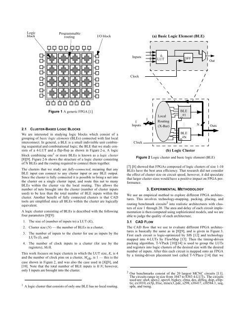
We are interested in studying logic blocks which consist of a<br />
grouping of basic logic elements (BLEs) connected with fast local<br />
interconnect. In general, a BLE is a small indivisible unit combining<br />
sequential <strong>and</strong> combinational logic; the BLE that we study consists<br />
of a 4-LUT <strong>and</strong> a flip-flop as shown in Figure 2-a. A logic<br />
block combining one 1 or more BLEs is known as a logic cluster<br />
[8][9]. Figure 2-b shows the structure of a logic cluster consisting<br />
of N BLEs <strong>and</strong> the routing required to connect them together.<br />
The clusters that we study are fully-connected, meaning that any<br />
BLE input can connect to any cluster input or any BLE output.<br />
Since the cluster is fully connected it is possible to bring a net into<br />
the cluster on a single cluster input, <strong>and</strong> route this net to many<br />
BLEs within the cluster via the local routing. This allows the<br />
number of nets brought into the cluster (number of cluster inputs<br />
used) to be less than the total number of BLE inputs within the<br />
cluster. Another benefit of fully connected clusters is that CAD<br />
tools are simplified since all BLEs within the cluster are logically<br />
equivalent.<br />
A logic cluster consisting of BLEs is described with the following<br />
four parameters [8][9]:<br />
1. The size of (number of inputs to) a LUT (K),<br />
2. Cluster size (N) — the number of BLEs in a cluster,<br />
3. The number of inputs to the cluster for use as inputs by the<br />
LUTs (I), <strong>and</strong><br />
4. The number of clock inputs to a cluster (for use by the<br />
registers), Mclk.<br />
This work focuses on logic clusters in which the LUT size, K, is 4<br />
<strong>and</strong> the number of clock pins on a cluster, M clk , is 1 — this is the<br />
case shown in Figure 2, <strong>and</strong> was also the case used in [8][9], <strong>and</strong><br />
[10]. Note that the total number of BLE inputs is K·N; however,<br />
only I inputs are brought into the cluster.<br />
1 A logic cluster that consists of only one BLE has no local routing.<br />
Inputs<br />
Clock<br />
I<br />
Inputs<br />
Clock<br />
I<br />
[7] [8] showed that FPGAs composed of logic clusters of size 1-10<br />
BLEs have the best area efficiency. That research did not consider<br />
the effect of cluster size on circuit speed, however, it did speculate<br />
that larger cluster sizes would have a positive impact on FPGA performance.<br />
3. EXPERIMENTAL METHODOLOGY<br />
We use an empirical method to explore different FPGA architectures.<br />
This involves technology-mapping, packing, placing, <strong>and</strong><br />
routing benchmark circuits 2 into realistic architectures with clusters<br />
of size 1 through 20. The area <strong>and</strong> delay of each circuit implementation<br />
is then computed using sophisticated models, <strong>and</strong> we are<br />
able to judge the quality of each architecture.<br />
3.1 CAD FLOW<br />
(a) Basic Logic Element (BLE)<br />
4-<br />
LUT<br />
Local<br />
Routing<br />
(X-Bar)<br />
DFF<br />
BLE<br />
#1<br />
. . .<br />
BLE<br />
#N<br />
(b) Logic Cluster<br />
Out<br />
Outs<br />
Figure 2 Logic cluster <strong>and</strong> basic logic element (BLE)<br />
The CAD flow that we use to evaluate different FPGA architectures<br />
is basically the same as in [8][9], <strong>and</strong> is given in Figure 3.<br />
First each circuit is logic-optimized by SIS [12] <strong>and</strong> technology<br />
mapped into 4-LUTs by FlowMap [13]. Then the timing-driven<br />
packing algorithm, T-VPack [10][14] is used to group the LUTs<br />
<strong>and</strong> registers into logic clusters of the desired size with the desired<br />
number of inputs. After this each circuit is mapped onto an FPGA<br />
by a timing-driven placement tool called T-VPlace [14] that we<br />
2 Our benchmarks consist of the 20 largest MCNC circuits [11].<br />
The circuits range in size from 1047 to 8383 4-LUTs. The circuits<br />
used are: alu4, apex2, apex4, bigkey, clma, des, diffeq, dsip, elliptic,<br />
ex1010, ex5p, frisc, misex3, pdc, s298, s38417, s38584.1, seq,<br />
spla, <strong>and</strong> tseng.<br />
N


