

FPGA a:nd CPLD Architectures: A Tutorial - IEEE Design & Test of ...
FPGA a:nd CPLD Architectures: A Tutorial - IEEE Design & Test of ...
FPGA a:nd CPLD Architectures: A Tutorial - IEEE Design & Test of ...

You also want an ePaper? Increase the reach of your titles
YUMPU automatically turns print PDFs into web optimized ePapers that Google loves.
o<strong>nd</strong>-sourced by other companies. The<br />
designation 16R8 means that the PAL<br />
has a maximum <strong>of</strong> 16 inputs (eight ded-<br />
icated inputs a<strong>nd</strong> eight input/outputs)<br />
a<strong>nd</strong> a maximum <strong>of</strong> eight outputs, a<strong>nd</strong><br />
that each output is registered (R) by a D<br />
flip-flop. Similarly, the 22V10 has a max-<br />
imum <strong>of</strong> 22 inputs a<strong>nd</strong> ten outputs. The<br />
V meansversatile-that is, each output<br />
can be registered or combinational.<br />
Another widely used a<strong>nd</strong> seco<strong>nd</strong>-<br />
sourced SPLD is the Altera Classic<br />
EP610. This device is similar in com-<br />
plexity to PALS, but <strong>of</strong>fers more flexibil-<br />
ity in the production <strong>of</strong> outputs a<strong>nd</strong> has<br />
larger AND a<strong>nd</strong> OR planes. The EPGlOs<br />
outputs can be registered, a<strong>nd</strong> the flip-<br />
flops are configurable as D, T, JK, or SR.<br />
Many other SPLD products are avail-<br />
able from a wide array <strong>of</strong> companies.<br />
All share common characteristics such<br />
as logic planes (AND, OR, NOR, or<br />
NAND), but each <strong>of</strong>fers unique features<br />
suitable for particular applications. A<br />
partial list <strong>of</strong> companies that <strong>of</strong>fer SPLDs<br />
includes AMD, Altera, ICT, Lattice,<br />
Cypress, a<strong>nd</strong> Philips-Signetics. The com-<br />
plexity <strong>of</strong> some <strong>of</strong> these SPLDs ap-<br />
proaches that <strong>of</strong> <strong>CPLD</strong>s.<br />
<strong>CPLD</strong>s. As we said earlier, <strong>CPLD</strong>s<br />
consist <strong>of</strong> multiple SPLD-like blocks on<br />
a single chip. However, <strong>CPLD</strong> products<br />
are much more sophisticated than<br />
SPLDs, even at the level <strong>of</strong> their basic<br />
SPLD-like blocks. In the following de-<br />
scriptions, we present sufficient details<br />
to compare competing products, em-<br />
phasizing the most widely used devices.<br />
Altera Max. Altera has developed<br />
three families <strong>of</strong> <strong>CPLD</strong> chips: Max 5000,<br />
7000, a<strong>nd</strong> 9000. We focus on the 7000<br />
series because <strong>of</strong> its wide use a<strong>nd</strong> state-<br />
<strong>of</strong>-the-art logic capacity a<strong>nd</strong> speed per-<br />
formance. Max 5000 represents an older<br />
technology that <strong>of</strong>fers a cost-effective<br />
solution; Max 9000 is similar to Max<br />
7000 but <strong>of</strong>fers higher logic capacity<br />
(the i<strong>nd</strong>ustry's highest for <strong>CPLD</strong>s). ' '<br />
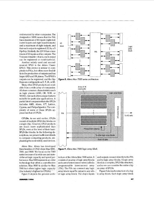
Figure 8 depicts the general archi-<br />
SUMMER 1996<br />
I10<br />
block<br />
PIA<br />
gure 8. Ahera Max 7000 series architecture.<br />
PIA<br />
Array <strong>of</strong> 16<br />
macrocells<br />
A<br />
gure 9. Ahera Max 7000 logic array block.<br />
cture <strong>of</strong> the Altera Max 7000 series. It<br />
Insists <strong>of</strong> an array <strong>of</strong> logic array blocks<br />
id a set <strong>of</strong> interconnect wires called a<br />
.ogrammable interconnect array<br />
'IA). The PIA can connect any logic<br />
ray block input %r output to any 0th-<br />
logic array block. The chip's inputs<br />
Logc<br />
array<br />
,I block<br />
-<br />
To I/O cells<br />
a<strong>nd</strong> outputs connect directly to the PIA<br />
a<strong>nd</strong> to logic array blocks. A logic array<br />
block is a complex, SPLD-like structure,<br />
a<strong>nd</strong> so we can consider the entire chip<br />
an array <strong>of</strong> SPLDs.<br />
Figure 9 showsthe structure <strong>of</strong> a log-<br />
ic array block. Each logic array block<br />
47


