Mid-infrared InAs/GaSb strained layer superlattice detectors with ...
Mid-infrared InAs/GaSb strained layer superlattice detectors with ...
Mid-infrared InAs/GaSb strained layer superlattice detectors with ...

You also want an ePaper? Increase the reach of your titles
YUMPU automatically turns print PDFs into web optimized ePapers that Google loves.
Home Search Collections Journals About Contact us My IOPscience<br />
<strong>Mid</strong>-<strong>infrared</strong> <strong>InAs</strong>/<strong>GaSb</strong> <strong>strained</strong> <strong>layer</strong> <strong>superlattice</strong> <strong>detectors</strong> <strong>with</strong> nBn design grown on a<br />
GaAs substrate<br />
This article has been downloaded from IOPscience. Please scroll down to see the full text article.<br />
2010 Semicond. Sci. Technol. 25 085010<br />
(http://iopscience.iop.org/0268-1242/25/8/085010)<br />
View the table of contents for this issue, or go to the journal homepage for more<br />
Download details:<br />
IP Address: 64.106.37.241<br />
The article was downloaded on 26/07/2010 at 17:29<br />
Please note that terms and conditions apply.
IOP PUBLISHING SEMICONDUCTOR SCIENCE AND TECHNOLOGY<br />
Semicond. Sci. Technol. 25 (2010) 085010 (4pp) doi:10.1088/0268-1242/25/8/085010<br />
<strong>Mid</strong>-<strong>infrared</strong> <strong>InAs</strong>/<strong>GaSb</strong> <strong>strained</strong> <strong>layer</strong><br />
<strong>superlattice</strong> <strong>detectors</strong> <strong>with</strong> nBn design<br />
grown on a GaAs substrate<br />
E Plis 1 , J B Rodriguez 2 , G Balakrishnan 1 ,YDSharma 1 ,HSKim 1 ,<br />
T Rotter 1 and S Krishna 1,3<br />
1 Center for High Technology Materials, Department of Electrical and Computer Engineering,<br />
University of New Mexico, Albuquerque NM 87106, USA<br />
2 Institut d’Electronique du Sud, UMR 5214 CNRS, Université Montpellier 2, Place Eugène Bataillon,<br />
34095 Montpellier Cedex 5, France<br />
E-mail: skrishna@chtm.unm.edu<br />
Received 9 April 2010, in final form 12 April 2010<br />
Published 23 July 2010<br />
Online at stacks.iop.org/SST/25/085010<br />
Abstract<br />
We report on a type-II <strong>InAs</strong>/<strong>GaSb</strong> <strong>strained</strong> <strong>layer</strong> <strong>superlattice</strong> (SLS) photodetector (λcut-off<br />
∼4.3 μm at 77 K) <strong>with</strong> nBn design grown on a GaAs substrate using interfacial misfit<br />
dislocation arrays to minimize threading dislocations in the active region. At 77 K and 0.1 V<br />
of the applied bias, the dark current density was equal to 6 × 10 −4 Acm −2 and the maximum<br />
specific detectivity D ∗ was estimated to 1.2 × 10 11 Jones (at 0 V). At 293 K, the zero-bias D ∗<br />
was found to be ∼10 9 Jones which is comparable to the nBn <strong>InAs</strong>/<strong>GaSb</strong> SLS detector grown<br />
on the <strong>GaSb</strong> substrate.<br />
1. Introduction<br />
Detectors based on type-II <strong>InAs</strong>/<strong>GaSb</strong> <strong>strained</strong> <strong>layer</strong><br />
<strong>superlattice</strong>s (SLSs) are being actively pursued as an<br />
alternative to mercury cadmium telluride and quantum well<br />
<strong>infrared</strong> technologies for the fabrication of high-performance<br />
<strong>infrared</strong> (IR) imagers. Flexibility of controlling the electronic<br />
band structure by variation of composition and thickness of the<br />
constituent <strong>layer</strong>s [1, 2], reduced Auger recombination rates<br />
[3] and improved quantum efficiency (QE) due to allowed<br />
normal incidence absorption together <strong>with</strong> enhanced material<br />
quality [4] enables the fabrication of high-performance focal<br />
plane arrays (FPAs) operating in the mid-wave IR (MWIR) [5]<br />
and long-wave IR [6] spectral regions.<br />
There are two constraints limiting the progress of present<br />
day SLS technology. First, relatively high levels of noise due to<br />
generation–recombination (G–R) and trap-assisted tunneling<br />
processes in the depletion region of the detector as well as<br />
leakage through surface states degrade the overall device<br />
performance. Various designs such as the M-structure [7],<br />
W-structure [8], graded bandgap [9] and p-π-M-n design [10]<br />
utilize the possibility of independent adjustment of conduction<br />
3 Author to whom any correspondence should be addressed.<br />
and valence band positions provided by the type-II band<br />
alignment and successfully suppress different dark current<br />
mechanisms. Recently proposed [11] and implemented on<br />
type-II SLS [12] nBn design concept <strong>with</strong> its counterparts [13]<br />
further extends this heterojunction engineering technique. It<br />
uses both a wide-band gap barrier to block majority carriers<br />
and a buried device structure effectively eliminating surface<br />
currents. In addition, it excludes the SRH G–R component<br />
of the dark current since it is intended to operate <strong>with</strong> n-type<br />
<strong>layer</strong>s in a flatband or <strong>with</strong> little depletion. <strong>InAs</strong>/<strong>GaSb</strong> MWIR<br />
SLSs single element <strong>detectors</strong> <strong>with</strong> nBn design show reduced<br />
dark current density by two orders of magnitude (at 77 K)<br />
compared to a conventional photodiode [14].<br />
The second constraint, which is the limiting factor in<br />
realizing large format SLS FPAs, is the lack of a high-quality,<br />
optically transparent larger area (4 inch diameter and beyond)<br />
substrates. Even though the <strong>GaSb</strong> substrate technology has<br />
made a significant progress in the past few years, the substrates<br />
are still not ‘epi-ready’ <strong>with</strong> a non-optimized oxide <strong>layer</strong> and<br />
macroscopic defects present on the growth surface. Moreover,<br />
the absorption coefficient of <strong>GaSb</strong> substrates is in the<br />
100 cm −1 range for IR radiation beyond 5 μm [15]. Thus,<br />
removal of the <strong>GaSb</strong> substrate is required for FPA applications.<br />
Moreover, the size of commercially available <strong>GaSb</strong> substrates<br />
0268-1242/10/085010+04$30.00 1 © 2010 IOP Publishing Ltd Printed in the UK & the USA
Semicond. Sci. Technol. 25 (2010) 085010 E Plis et al<br />
is less than 3 inch in diameter due to limited demand in the<br />
semiconductor industry. To overcome this issue the use of<br />
alternative substrates like GaAs [16–18] for<strong>InAs</strong>/<strong>GaSb</strong> SLS<br />
growth has been proposed. The absorption coefficient of<br />
GaAs is nearly two orders of magnitude lower than that of<br />
<strong>GaSb</strong>. In addition, large format epi-ready GaAs substrates<br />
are commercially available (6 inch in diameter) which is<br />
advantageous for the cost reduction in the mass production<br />
of IR FPAs.<br />
Unfortunately, due to an ∼7.8% lattice mismatch between<br />
GaAs and <strong>GaSb</strong> the direct growth of <strong>GaSb</strong> on GaAs gives rise<br />
to a high misfit dislocation density (10 9 cm −2 )[19] atthe<br />
<strong>GaSb</strong>/GaAs interface and throughout the epitaxial film. In<br />
order to realize high-performance <strong>InAs</strong>/<strong>GaSb</strong> SLS <strong>detectors</strong><br />
on GaAs substrates, it is necessary to develop growth methods<br />
to accommodate strain and decrease the dislocation density.<br />
Among them is a low-temperature nucleation technique<br />
[20] utilized for the demonstration of type-II SLS MWIR<br />
photodiode <strong>with</strong> p-i-n design grown on GaAs substrates. In<br />
this paper, we demonstrate an <strong>InAs</strong>/<strong>GaSb</strong> SLS detector <strong>with</strong><br />
nBn design (λcut-off ∼ 4.3 μm, 77 K) grown on a GaAs<br />
substrate <strong>with</strong> a significantly different growth scheme termed<br />
as the interfacial misfit dislocation (IMF) array technique<br />
[21, 22].<br />
2. Experimental procedure<br />
The detector structures were grown using a solid source<br />
molecular beam epitaxy (MBE) VG-80 system on semiinsulating<br />
epi-ready (1 0 0) 3 inch GaAs substrates. First, a<br />
1 μm <strong>GaSb</strong> buffer <strong>layer</strong> was deposited on top of the GaAs<br />
substrate <strong>with</strong> the IMF technique. This growth mode involves<br />
establishing a (2 × 8) Sb reconstruction on GaAs (1 0 0)<br />
followed by direct growth of <strong>GaSb</strong>. As was reported in<br />
previous publications [21, 22] such a process establishes an<br />
array of 90 ◦ interfacial misfit dislocations at the <strong>GaSb</strong>/GaAs<br />
interface allowing the growth of spontaneously relaxed and<br />
extremely low-defect density <strong>GaSb</strong> (1 × 10 6 cm −2 )onGaAs.<br />
Then a 500 nm thick bottom contact <strong>layer</strong> consisting of 8 ML<br />
<strong>InAs</strong>/8 ML <strong>GaSb</strong> SLS <strong>with</strong> Si-doped <strong>InAs</strong> <strong>layer</strong>s (n = 4 ×<br />
10 18 cm −3 ) was grown followed by a 100 nm Al0.2Ga0.8Sb<br />
non-intentionally doped (n.i.d.) barrier <strong>layer</strong>. Next, an<br />
∼2.5 μm thick (520 periods) n.i.d. absorption region was<br />
grown <strong>with</strong> the same <strong>superlattice</strong> composition and thickness<br />
as the bottom contact <strong>layer</strong>. The SLS absorption region<br />
is residual n-type <strong>with</strong> a carrier concentration in the low<br />
10 16 cm −3 at room temperature [23, 24]. The structure was<br />
capped by a 100 nm thick top contact <strong>layer</strong> made of the<br />
same material as the bottom contact <strong>layer</strong>. The SLS growth<br />
conditions were similar to the procedure reported previously<br />
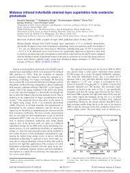
[12]. The inset to figure 1 shows an atomic force micrograph<br />
(AFM) of the detector structure over a 20 × 20 μm 2 area<br />
and root-mean-square (rms) surface roughness of 2 nm. The<br />
material of the barrier <strong>layer</strong> has a wider bandgap than absorbing<br />
and contact <strong>layer</strong>s in order to provide nearly zero valence<br />
band offset and a large conduction band offset. As a result, the<br />
majority carrier (electrons) current between the two electrodes<br />
2<br />
Figure 1. Normalized temperature-dependent spectral response<br />
from the <strong>InAs</strong>/<strong>GaSb</strong> SLS detector <strong>with</strong> nBn design. The inset<br />
shows an AFM of the full detector structure over 20 × 20 μm 2 areas.<br />
(This figure is in colour only in the electronic version)<br />
is blocked by the large energy offset, while there is no barrier<br />
for photogenerated minority carriers (holes).<br />
The material was processed into normal incidence 410 ×<br />
410 μm2 single pixel devices <strong>with</strong> a 300 μm diameter circular<br />
aperture. The processing was initiated by mesa definition<br />
etching in an inductively coupled plasma reactor <strong>with</strong> BCl3<br />
gas. Subsequently, ohmic contacts were made by depositing<br />
Ti/Pt/Au on the bottom and top contact <strong>layer</strong>s of the <strong>detectors</strong>.<br />
After contact metallization, the fabricated devices were wire<br />
bonded to a leadless chip carrier for further characterization.<br />
The 50% cut-off wavelength of the processed devices<br />
was obtained from spectral response measurements performed<br />
using a Fourier transform IR spectrometer <strong>with</strong> a glow-bar<br />
black body source. Normalized spectral response was obtained<br />
by dividing the photocurrent of the SLS detector <strong>with</strong> that<br />
obtained using a standard deuterated triglycine sulfate thermal<br />
detector. The responsivity and QE of devices were measured<br />
using a Mikron blackbody at 500 ◦C. Specific detectivity D∗ of the device was evaluated using the following equation:<br />
D ∗ = Ri · � Ad · �f / iN, (1)<br />
where Ri is the measured responsivity, Ad is the electrical area<br />
of the diode, and iN is the noise current obtained by integrating<br />
the noise spectrum in a bandwidth of �f beyond the corner<br />
frequency.<br />
3. Results and discussion<br />
The detector 50% cut-off wavelength was found to be 4.3 μm<br />
at 77 K (Vb = 0.5 V). Figure 1 shows the normalized spectral<br />
response of the detector at different temperatures. It should<br />
be noted that the bias was taken as positive when the voltage<br />
polarity was positive on the top contact. The applied bias did<br />
not significantly affect the behavior of the spectral response<br />
curves.<br />
Current voltage (IV) characteristics were measured for<br />
temperatures ranging from 77 to 293 K and are shown in
Semicond. Sci. Technol. 25 (2010) 085010 E Plis et al<br />
Table 1. Performance comparison of <strong>detectors</strong> grown on different substrates <strong>with</strong> conventional p-i-n or nBn designs.<br />
Parameter nBn on GaAs nBn on <strong>GaSb</strong> [12] p-i-n on GaAs [16] p-i-n on <strong>GaSb</strong> [25]<br />
λ50%cut−off (μm) 4.3 (77 K) 5.1 (250 K) 5.2 (300 K) ∼4.04 (77 K) ∼4.5 (260 K) 4.2 (77 K) 4.6 (250 K)<br />
Dark current density (A cm −2 ) 6× 10 −4 at Vb = 0.1 V 2 × 10 −3 at Vb =−0.5 V 3 × 10 −4 at Vb =−0.3 V 2 × 10 −5 at Vb = –0.3 V<br />
(77 K)<br />
Dark current density (A cm −2 ) 3.6 at Vb = 0.1 V 2 at Vb =−0.5 V 3 at Vb =−0.5 V 0.18 at Vb = –0.1 V<br />
(293 K)<br />
QE (%) (77 K, λ = 4.0 μm) 15 at Vb = 3V 20atVb =−0.3 V 17 at Vb = 0V 18atVb =−0.5 V<br />
Zero-bias D ∗ at 77 K (Jones) 10 11 at 4 μm N/A ∼3 × 10 11 at 4 μm 1.9 × 10 12 at 4 μm<br />
Zero-bias D ∗ at 293 K (Jones) 10 9 at 4 μm 10 9 at 4.5 μm ∼7 × 10 8 at 4 μm 1.9 × 10 9 at 4 μm<br />
Figure 2. Dark current density versus applied bias at different<br />
temperatures for the nBn detector <strong>with</strong> 410 × 410 μm 2 mesa size.<br />
The normal operating bias for the nBn detector is the forward bias<br />
voltage which is defined as a positive voltage applied to the bottom<br />
contact.<br />
figure 2. At 77 K and 0.1 V of the applied bias, the dark current<br />
density was 6 × 10 −4 Acm −2 corresponding to a differentialresistance-area<br />
product at zero bias (R0A) of 268 � cm 2 .At<br />
293 K and the same applied bias, the dark current density was<br />
3.6 A cm −2 <strong>with</strong> R0A of 2.2 × 10 −2 � cm 2 . The measured<br />
values of R0A in our device are worse compared <strong>with</strong> those<br />
for the recently reported <strong>InAs</strong>/<strong>GaSb</strong> p-i-n <strong>detectors</strong> grown on<br />
GaAs substrates <strong>with</strong> a 4 μm <strong>GaSb</strong> buffer <strong>layer</strong> [16]. Since<br />
the nBn detector is a minority carrier photoconductor, R0A is<br />
not a very good metric for such devices. Comparison of the<br />
measured values of dark current densities under operational<br />
bias conditions for our device, the nBn detector grown on<br />
<strong>GaSb</strong> [12] and p-i-n <strong>detectors</strong> grown on GaAs [16] and <strong>GaSb</strong><br />
[25] substrates is shown in table 1. At 77 K, our detector<br />
demonstrates performance comparable <strong>with</strong> nBn <strong>detectors</strong><br />
grown on <strong>GaSb</strong> [12] and p-i-n <strong>detectors</strong> grown on the GaAs<br />
substrate [16]. However, it showed a factor of ∼30 higher dark<br />
current density than p-i-n <strong>detectors</strong> grown on <strong>GaSb</strong> reported<br />
by our group earlier [25]. We attribute it to the longer cutoff<br />
wavelength of our device and possible imperfection of<br />
the IMF technique. Currently, an optimization of the IMF<br />
technique for the SLS <strong>detectors</strong> is being undertaken in our<br />
group.<br />
At 77 K and zero bias the device exhibited QE of 11%<br />
(figure 3). The maximum value of QE was equal to 15% at<br />
Vb = 3 V. Corresponding values of responsivity were<br />
3<br />
Figure 3. Quantum efficiency and responsivity measured for the<br />
<strong>InAs</strong>/<strong>GaSb</strong> nBn detector at 77 K and 4 μm.<br />
Figure 4. Noise current and detectivity obtained from the<br />
<strong>InAs</strong>/<strong>GaSb</strong> nBn detector at 77 K using a calibrated blackbody at<br />
500 ◦ C.<br />
0.35 A W −1 (zero bias) and ∼0.5 A W −1 (Vb = 3 V). It should<br />
be noted that QE remains constant in the (0–0.6) V bias region<br />
and it slightly increases at 0.6 V. This bias dependence of QE is<br />
probably due to the fact that not all the carriers are collected at<br />
lower bias voltages, which is attributed to the presence of small<br />
valence band offset. Further optimization of composition and<br />
the doping level of the ternary barrier <strong>layer</strong> are required to<br />
achieve a zero-energy valence band offset between the barrier<br />
and SLS forming the absorption region of the device.<br />
Finally, the specific detectivity D ∗ of the device was<br />
evaluated at 4 μm and the results are summarized in figure 4.
Semicond. Sci. Technol. 25 (2010) 085010 E Plis et al<br />
At 77 K the maximum D ∗ was found under zero bias and equal<br />
to 1.2 × 10 11 Jones which is similar to the performance of other<br />
MWIR type-II SLS grown on GaAs substrates [16] (∼3 ×<br />
10 11 Jones). At 293 K, D ∗ under zero bias was equal to<br />
∼10 9 Jones, which is slightly higher than D ∗ demonstrated<br />
by <strong>InAs</strong>/<strong>GaSb</strong> SLS <strong>detectors</strong> <strong>with</strong> p-i-n design grown on<br />
the GaAs substrate [16] (7× 10 8 Jones) and comparable<br />
<strong>with</strong> performance of nBn <strong>detectors</strong> grown on the <strong>GaSb</strong><br />
substrate [12] (10 9 Jones). Detailed performance comparison<br />
of <strong>detectors</strong> grown on different substrates <strong>with</strong> conventional<br />
p-i-n or nBn designs is shown in table 1.<br />
4. Conclusions<br />
In conclusion, we report an <strong>InAs</strong>/<strong>GaSb</strong> SLS detector <strong>with</strong><br />
nBn design operating in the MWIR wavelength range (λcut-off<br />
∼4.3 μm at 77 K) grown on a GaAs substrate <strong>with</strong> the IMF<br />
technique. QE between 11% and 18%, and specific detectivity<br />
D ∗ ∼10 11 Jones at 77 K and 4 μm were demonstrated. At<br />
293 K, D ∗ under the same conditions was equal to ∼10 9 Jones<br />
which is comparable to the p-i-n <strong>InAs</strong>/<strong>GaSb</strong> SLS <strong>detectors</strong><br />
grown on the GaAs substrate and the nBn <strong>InAs</strong>/<strong>GaSb</strong> SLS<br />
detector grown on <strong>GaSb</strong> substrates, and <strong>with</strong>in a factor of<br />
2 lower than D ∗ measured for the MWIR p-i-n detector grown<br />
on the <strong>GaSb</strong> substrate.<br />
Acknowledgments<br />
The authors would like to acknowledge support from AFOSR<br />
Contract FA9550-09-1-0231 and AFRL Contract FA9453-07-<br />
C-0171.<br />
References<br />
[1] Smith D L and Mailhiot C 1987 J. Appl. Phys. 62 2545<br />
[2] Haugan H J, Szmulowicz F, Brown G J and Mahalingam K<br />
2004 Appl. Phys. Lett. 84 5410<br />
[3] Youngdale E R, Meyer J R, Hoffman C A, Bartoli F J,<br />
Grein C H, Young P M, Ehrenreich H, Miles R H and<br />
Chow D H 2004 Appl. Phys. Lett. 64 3160<br />
[4] Walther M, Rehm R, Schmitz J, Rutz F, Fleissner J and<br />
Ziegler J 2008 Proc. SPIE 6940 69400A<br />
[5] Walther M, Schmitz J, Rehm R, Kopta S, Fuchs F, Fleibner J,<br />
Cabanski W and Ziegler J 2005 J. Cryst. Growth<br />
278 156<br />
4<br />
[6] Hill C J, Soibel A, Keo S A, Mumolo J M, Ting D Z,<br />
Gunapala S D, Rhiger D R, Kvaas R E and Harris S F 2009<br />
Proc. SPIE 7298 729804<br />
[7] Nguyen B M, Hoffman D, Delaunay P Y, Huang E K W,<br />
Razeghi M and Pellegrino J 2008 Appl. Phys. Lett.<br />
93 163502<br />
[8] Aifer E H, Tischler J G, Warner J H, Vurgaftman I,<br />
Bewley W W, Meyer J R, Kim J C, Whitman J L,<br />
Canedy C L and Jackson E M 2006 Appl. Phys. Lett.<br />
89 053519<br />
[9] Vurgaftman I, Aifer E H, Canedy C L, Tischler J G,<br />
Meyer J R, Warner J H, Jackson E M, Hildebrandt G<br />
and Sullivan G J 2006 Appl. Phys. Lett. 89 121114<br />
[10] Nguyen B M, Hoffman D, Delaunay P Y and Razeghi M 2007<br />
Appl. Phys. Lett. 91 163511<br />
[11] Maimon S and Wicks G W 2006 Appl. Phys. Lett. 89 1511009<br />
[12] Rodriguez J B, Plis E, Bishop G, Sharma Y D, Kim H,<br />
Dawson L R and Krishna S 2007 Appl. Phys. Lett.<br />
91 043514<br />
[13] Nguyen B M, Bogdanov S, Abdollahi Pour S and Razeghi M<br />
2009 Appl. Phys. Lett. 95 183502<br />
[14] Bishop G, Plis E, Rodriguez J B, Sharma Y D, Kim H S,<br />
Dawson L R and Krishna D 2008 J. Vac. Sci. Technol. B<br />
26 1145<br />
[15] Chandola A, Pino R and Dutta P S 2005 Semicond. Sci.<br />
Technol. 20 886<br />
[16] Nguyen B M, Hoffman D, Huang E K W, Bogdanov D,<br />
Delaunay P Y, Razeghi M and Tidrow M Z 2009 Appl.<br />
Phys. Lett. 94 223506<br />
[17] Zhang X B, Ryou J H, Dupuis R D, Petschke A, Mou S,<br />
Chuang S L, Xu C and Hsieh K C 2006 Appl. Phys. Lett.<br />
88 072104<br />
[18] Tang B, Xu Y Q, Zhou Z Q, Hao R T, Wang G W, Ren Z W<br />
and Niu Z C 2009 Chin. Phys. Lett. 26 028102<br />
[19] Johnson G R, Cavenett B C, Kerr T M, Kirby P B and Wood C<br />
E C 1988 Semicond. Sci. Technol. 3 1157<br />
[20] Michel E, Mohseni H, Kim J D, Wojkowski J, Sandven J, Xu<br />
J, Razeghi M, Bredthauer R, Vu P, Mitchel W and Ahoujja<br />
M 1997 Appl. Phys. Lett. 71 1071<br />
[21] Huang S H, Balakrishnan G, Khoshakhlagh A, Jallipalli A,<br />
Dawson L R and Huffaker D L 2006 Appl. Phys. Lett.<br />
88 131911<br />
[22] Jallipalli A, Nunna K, Kutty M N, Balakrishnan G, Dawson L<br />
R and Huffaker D L 2009 Appl. Phys. Lett. 95 202107<br />
[23] Hood A, Hoffman D, Wei Y, Fuchs F and Razeghi M 2006<br />
Appl. Phys. Lett. 88 052112<br />
[24] Cervera C, Rodriguez J B, Perez J P, Aït-Kaci H, Chaghi R,<br />
Konczewicz L, Contreras S and Christol P 2009 J. Appl.<br />
Phys. 106 033709<br />
[25] Plis E, Rodriguez J B, Kim H S, Bishop G, Sharma Y, Dawson<br />
R, Lee S J, Jones C E, Gopal V and Krishna S 2007 Appl.<br />
Phys. Lett. 91 133512