Download PDF - Carl Zeiss
Download PDF - Carl Zeiss
Download PDF - Carl Zeiss

Create successful ePaper yourself
Turn your PDF publications into a flip-book with our unique Google optimized e-Paper software.
Nanostructuring Using 3D Deposition Lith<br />
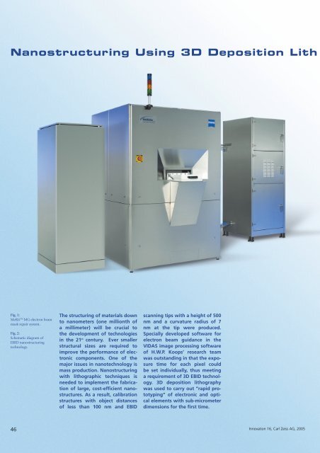
Fig. 1:<br />
MeRit TM MG electron beam<br />
mask repair system.<br />
Fig. 2:<br />
Schematic diagram of<br />
EBID nanostructuring<br />
technology.<br />
46<br />
The structuring of materials down<br />
to nanometers (one millionth of<br />
a millimeter) will be crucial to<br />
the development of technologies<br />
in the 21 st century. Ever smaller<br />
structural sizes are required to<br />
improve the performance of electronic<br />
components. One of the<br />
major issues in nanotechnology is<br />
mass production. Nanostructuring<br />
with lithographic techniques is<br />
needed to implement the fabrication<br />
of large, cost-efficient nanostructures.<br />
As a result, calibration<br />
structures with object distances<br />
of less than 100 nm and EBID<br />
scanning tips with a height of 500<br />
nm and a curvature radius of 7<br />
nm at the tip were produced.<br />
Specially developed software for<br />
electron beam guidance in the<br />
VIDAS image processing software<br />
of H.W.P. Koops’ research team<br />
was outstanding in that the exposure<br />
time for each pixel could<br />
be set individually, thus meeting<br />
a requirement of 3D EBID technology.<br />
3D deposition lithography<br />
was used to carry out “rapid prototyping”<br />
of electronic and optical<br />
elements with sub-micrometer<br />
dimensions for the first time.<br />
Innovation 16, <strong>Carl</strong> <strong>Zeiss</strong> AG, 2005