

Switch Mode Battery Eliminator Based on a PIC16C72A - Microchip
Switch Mode Battery Eliminator Based on a PIC16C72A - Microchip
Switch Mode Battery Eliminator Based on a PIC16C72A - Microchip

You also want an ePaper? Increase the reach of your titles
YUMPU automatically turns print PDFs into web optimized ePapers that Google loves.
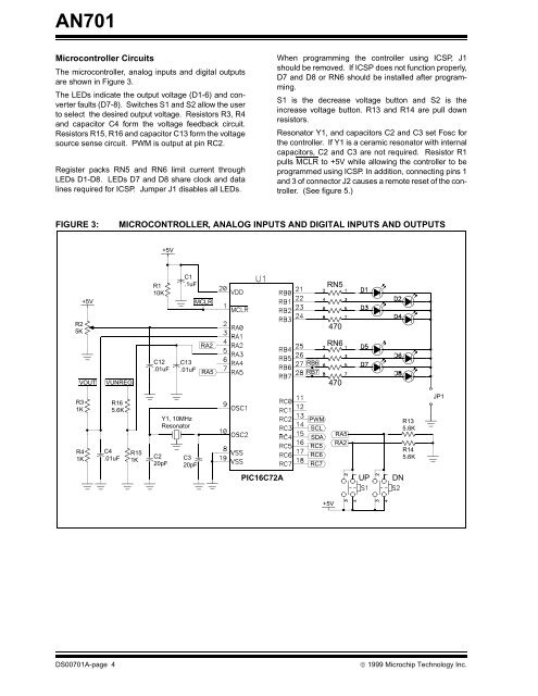
AN701<br />
Microc<strong>on</strong>troller Circuits<br />
The microc<strong>on</strong>troller, analog inputs and digital outputs<br />
are shown in Figure 3.<br />
The LEDs indicate the output voltage (D1-6) and c<strong>on</strong>verter<br />
faults (D7-8). <str<strong>on</strong>g>Switch</str<strong>on</strong>g>es S1 and S2 allow the user<br />
to select the desired output voltage. Resistors R3, R4<br />
and capacitor C4 form the voltage feedback circuit.<br />
Resistors R15, R16 and capacitor C13 form the voltage<br />
source sense circuit. PWM is output at pin RC2.<br />
Register packs RN5 and RN6 limit current through<br />
LEDs D1-D8. LEDs D7 and D8 share clock and data<br />
lines required for ICSP. Jumper J1 disables all LEDs.<br />
When programming the c<strong>on</strong>troller using ICSP, J1<br />
should be removed. If ICSP does not functi<strong>on</strong> properly,<br />
D7 and D8 or RN6 should be installed after programming.<br />
S1 is the decrease voltage butt<strong>on</strong> and S2 is the<br />
increase voltage butt<strong>on</strong>. R13 and R14 are pull down<br />
resistors.<br />
Res<strong>on</strong>ator Y1, and capacitors C2 and C3 set Fosc for<br />
the c<strong>on</strong>troller. If Y1 is a ceramic res<strong>on</strong>ator with internal<br />
capacitors, C2 and C3 are not required. Resistor R1<br />
pulls MCLR to +5V while allowing the c<strong>on</strong>troller to be<br />
programmed using ICSP. In additi<strong>on</strong>, c<strong>on</strong>necting pins 1<br />
and 3 of c<strong>on</strong>nector J2 causes a remote reset of the c<strong>on</strong>troller.<br />
(See figure 5.)<br />
FIGURE 3: MICROCONTROLLER, ANALOG INPUTS AND DIGITAL INPUTS AND OUTPUTS<br />
R2<br />
5K<br />
VOUT<br />
R3<br />
1K<br />
R4<br />
1K<br />
+5V<br />
VUNREG<br />
R16<br />
5.6K<br />
C4<br />
.01uF<br />
R15<br />
1K<br />
R1<br />
10K<br />
+5V<br />
C12<br />
.01uF<br />
Y1, 10MHz<br />
Res<strong>on</strong>ator<br />
C2<br />
20pF<br />
C1<br />
.1uF<br />
C13<br />
.01uF<br />
C3<br />
20pF<br />
MCLR<br />
RA2<br />
RA5<br />
<strong>PIC16C72A</strong><br />
UP DN<br />
DS00701A-page 4 © 1999 <strong>Microchip</strong> Technology Inc.<br />
RB6<br />
RB7<br />
PWM<br />
SCL<br />
SDA<br />
RC5<br />
RC6<br />
RC7<br />
RN5<br />
470<br />
RN6<br />
+5V<br />
470<br />
RA5<br />
RA2<br />
R13<br />
5.6K<br />
R14<br />
5.6K<br />
JP1


