Alumnus Jahrbuch 2009 (3,0 MB) - Physik-alumni.de
Alumnus Jahrbuch 2009 (3,0 MB) - Physik-alumni.de
Alumnus Jahrbuch 2009 (3,0 MB) - Physik-alumni.de

Erfolgreiche ePaper selbst erstellen
Machen Sie aus Ihren PDF Publikationen ein blätterbares Flipbook mit unserer einzigartigen Google optimierten e-Paper Software.
Silicon spin transistor<br />
Electrons have charge and spin. The<br />
mo<strong>de</strong>rn information technology uses<br />
the charge to store and process information.<br />
But the spin is catching up.<br />
There are several reasons for that. For<br />
one, the electron spin can control the<br />
transport of charge. Another reason is<br />
the fact that the information stored in<br />
the electron spin could survive sufficiently<br />
long to be processed in nanoscale<br />
<strong>de</strong>vices. The spin typically survives<br />
for nanoseconds (and can be transported<br />
for micrometers) while the electron<br />
momentum or velocity only up to picoseconds.<br />
Finally, the electron spin is a<br />
most natural qubit---a two-level quantum<br />
mechanical system that can be<br />
controlled coherently to process quantum<br />
information---projecting the potential<br />
of the spin in quantum computing.<br />
There are also fundamental<br />
aspects the electron spin brings into<br />
the solid-state environment. When one<br />
hears “spin” one most likely thinks of<br />
“ferromagnetism” or magnetism in general.<br />
The spin is also there to control<br />
the statistics: the Pauli principle leads<br />
to the Fermi-Dirac population distribution,<br />
but this is somehow given and<br />
the spin is rather passive in this role. In<br />
a ferromagnet the spin works its way<br />
through the exchange interaction. But<br />
there is another spin-<strong>de</strong>pen<strong>de</strong>nt interaction,<br />
the relativistic spin-orbit coupling<br />
which, while typically much smaller<br />
than the exchange one which gives<br />
ferromagnetism, leads to many fascinating<br />
phenomena, many of them observed<br />
in the recent years only. We still<br />
have a limited knowledge of what the<br />
ramifications of spin-orbit coupling are<br />
for the electronic properties of solid<br />
state systems, different material compositions,<br />
and different dimensionalities.<br />
But one thing is clear: as the name<br />
suggests, the interaction couples the<br />
spin and orbital <strong>de</strong>grees of freedom.<br />
In the same token, it couples ferromagnetism<br />
and transport, providing the<br />
control knob.<br />
The field encompassing both<br />
the fundamental and applied aspects<br />
of the electron spin in the solid-state<br />
environment is called spintronics. The<br />
major goals are finding ways to control<br />
the electric current by the spin and,<br />
vice versa, finding ways to control the<br />
spin by electrical means. The most successful<br />
spintronics <strong>de</strong>vices are based<br />
on the giant magnetoresistance effect<br />
(GMR). This effect, which earned its<br />
discoverers Albert Fert and Peter Grünberg<br />
the Nobel Prize in Physics in 2007,<br />
is about the changes in the electrical<br />
resistance in systems comprising ferromagnetic<br />
layers. If the magnetizations<br />
of the layers are parallel, the resistance<br />
is low. If they are antiparallel, the resistance<br />
is large.<br />
The GMR-based <strong>de</strong>vices had been<br />
used to launch a revolution in the magnetic<br />
storage (computer hard disk<br />
read heads). Nowadays the read heads<br />
use a similar effect, called the tunneling<br />
magnetoresistance (TMR), which works<br />
the same way as the GMR but in the<br />
tunneling regime.<br />
Both GMR and TMR <strong>de</strong>vices are<br />
based on ferromagnetic metals. Thus<br />
far, no useful spintronic <strong>de</strong>vice based<br />
on semiconductors has been ma<strong>de</strong>.<br />
There have been many experimental<br />
<strong>de</strong>monstrations of <strong>de</strong>vice-like structures,<br />
but it is yet too early to say which<br />
scheme of a semiconductor spintronic<br />
<strong>de</strong>vice will win a place in industry.<br />
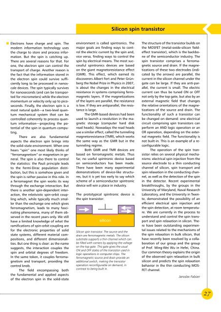
The prototypical spintronic <strong>de</strong>vice is<br />
the spin transistor:<br />
Silicon spin transistor. The source and the<br />
drain are ferromagnetic metals. The silicon<br />
substrate supports a thin channel which can<br />
be filled with carriers by applying the voltage<br />
on the top gate. This gate gives the usual<br />
ON and OFF states of the transistor used in<br />
logic operations in computer chips. The<br />
ferromagnetic source and drain provi<strong>de</strong> an<br />
additional switch, making the transistor<br />
operation reconfigurable on <strong>de</strong>mand, in<br />
contrast to being built in.<br />
The structure of the transistor builds on<br />
the MOSFET (metal-oxi<strong>de</strong>-silicon fiel<strong>de</strong>ffect<br />
transistor), which is the backbone<br />
of the semiconductor industry. The<br />
spin transistor comprises a ferromagnetic<br />
source and drain. If the magnetizations<br />
of these two electro<strong>de</strong>s (indicated<br />
by the arrows) are parallel, the<br />
current in the silicon channel un<strong>de</strong>r the<br />
gate can be large. If they are anti-parallel,<br />
the current is small. The electric<br />
current can thus be tuned ON or OFF<br />
not only by the top gate, but also by an<br />
external magnetic field that changes<br />
the relative orientations of the magnetizations<br />
of the source and drain. The<br />
functionality of such a transistor can<br />
be changed on <strong>de</strong>mand: one electrical<br />
circuit comprising spin transistors can<br />
perform an AND logic operation or an<br />
OR operation, <strong>de</strong>pending on the external<br />
magnetic field. The functionality is<br />
not built-in. This is an example of a reconfigurable<br />
logic.<br />
The operation of the spin transistor<br />
relies on several physical mechanisms:<br />
electrical spin injection from the<br />
source electro<strong>de</strong> to a thin conducting<br />
channel of silicon, spin transport and<br />
spin relaxation in the conducting channel,<br />
as well as the <strong>de</strong>tection of the spin<br />
in the <strong>de</strong>tector. Recent experimental<br />
breakthroughs, by the groups in the<br />
University of Maryland, Naval Research<br />
Laboratory, and the University in Twente,<br />
<strong>de</strong>monstrated the possibility of an<br />
efficient electrical spin injection and<br />
the spin <strong>de</strong>tection, at room temperature.<br />
We are currently in the process to<br />
un<strong>de</strong>rstand and control the spin transport<br />
and spin relaxation in silicon. There<br />
have been outstanding experimental<br />
issues related to the mechanisms of<br />
the spin relaxation in bulk silicon, that<br />
have recently been resolved by a collaboration<br />
of our group and the group<br />
of Prof. Ming-Wei Wu in Hefei, China.<br />
Our common theory explains the origin<br />
of the observed spin relaxation in bulk<br />
silicon and predicts the spin relaxation<br />
behavior in the thin conducting MOS-<br />
FET channel.<br />
Jaroslav Fabian<br />
27