6. Comprehensive List of Publications Prof. Dr. Daniel Erni
6. Comprehensive List of Publications Prof. Dr. Daniel Erni
6. Comprehensive List of Publications Prof. Dr. Daniel Erni

Create successful ePaper yourself
Turn your PDF publications into a flip-book with our unique Google optimized e-Paper software.
<strong>6.</strong> <strong>Comprehensive</strong> <strong>List</strong> <strong>of</strong> <strong>Publications</strong><br />
Pr<strong>of</strong>. <strong>Dr</strong>. <strong>Daniel</strong> <strong>Erni</strong><br />
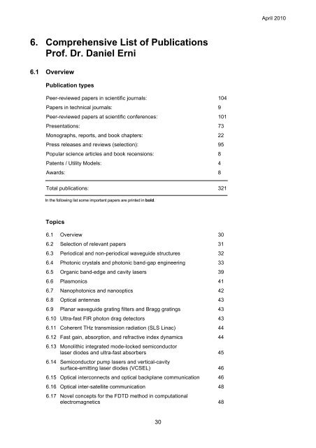
<strong>6.</strong>1 Overview<br />
Publication types<br />
Peer-reviewed papers in scientific journals: 104<br />
Papers in technical journals: 9<br />
Peer-reviewed papers at scientific conferences: 101<br />
Presentations: 73<br />
Monographs, reports, and book chapters: 22<br />
Press releases and reviews (selection): 95<br />
Popular science articles and book recensions: 8<br />
Patents / Utility Models: 4<br />
Awards: 8<br />
Total publications: 321<br />
In the following list some important papers are printed in bold.<br />
Topics<br />
<strong>6.</strong>1 Overview 30<br />
<strong>6.</strong>2 Selection <strong>of</strong> relevant papers 31<br />
<strong>6.</strong>3 Periodical and non-periodical waveguide structures 32<br />
<strong>6.</strong>4 Photonic crystals and photonic band-gap engineering 33<br />
<strong>6.</strong>5 Organic band-edge and cavity lasers 39<br />
<strong>6.</strong>6 Plasmonics 41<br />
<strong>6.</strong>7 Nanophotonics and nanooptics 42<br />
<strong>6.</strong>8 Optical antennas 43<br />
<strong>6.</strong>9 Planar waveguide grating filters and Bragg gratings 43<br />
<strong>6.</strong>10 Ultra-fast FIR photon drag detectors 43<br />
<strong>6.</strong>11 Coherent THz transmission radiation (SLS Linac) 44<br />
<strong>6.</strong>12 Fast gain, absorption, and refractive index dynamics<br />
<strong>6.</strong>13 Monolithic integrated mode-locked semiconductor<br />
44<br />
laser diodes and ultra-fast absorbers 45<br />
<strong>6.</strong>14 Semiconductor pump lasers and vertical-cavity<br />
surface-emitting laser diodes (VCSEL) 46<br />
<strong>6.</strong>15 Optical interconnects and optical backplane communication 46<br />
<strong>6.</strong>16 Optical inter-satellite communication 48<br />
<strong>6.</strong>17 Novel concepts for the FDTD method in computational<br />
electromagnetics 48<br />
30<br />
April 2010
<strong>6.</strong>18 RF technology and microwave electronics 49<br />
<strong>6.</strong>19 Electromagnetic metamaterials 49<br />
<strong>6.</strong>20 Process tomography and inverse scattering in natural soils 50<br />
<strong>6.</strong>21 General electrical engineering 50<br />
<strong>6.</strong>22 Science and Technology Studies (STS) 50<br />
<strong>6.</strong>23 Press releases and reviews (selection) 51<br />
<strong>6.</strong>24 Miscellaneaous 54<br />
<strong>6.</strong>25 Monographs and lecture notes 55<br />
<strong>6.</strong>26 Popular science articles and book recensions 55<br />
<strong>6.</strong>27 Patents / Utility Models 56<br />
<strong>6.</strong>28 Awards 56<br />
<strong>6.</strong>2 Selection <strong>of</strong> relevant papers<br />
31<br />
April 2010<br />
� E. Moreno, D. <strong>Erni</strong>, Ch. Hafner, and R. Vahldieck, "Multiple multipole method with automatic multipole<br />
setting applied to the simulation <strong>of</strong> surface plasmons in metallic nanostructures," J. Opt. Soc. Am. A,<br />
vol. 19, no. 1, pp. 101-111, Jan. 2002.<br />
� E. Moreno, D. <strong>Erni</strong>, and Ch. Hafner, "Band structure computations <strong>of</strong> metallic photonic crystals with<br />
the multiple multipole method," Phys. Rev. B, vol. 65, no. 15, pp. 155120-1-10, April 15, 2002.<br />
also in: � Virtual Journal <strong>of</strong> Nanoscale Science & Technology, vol. 5, no. 16, April 22, 2002.<br />
� Nanojournal, no. 45, Art. no. 3569, May 19, 2002.<br />
� J. Smajic, Ch. Hafner, and D. <strong>Erni</strong>, "Design and optimization <strong>of</strong> an achromatic photonic crystal bend,"<br />
Opt. Express, vol. 11, no. 12, pp. 1378-1384, June 16, 2003.<br />
also in: � Virtual Journal <strong>of</strong> Nanoscale Science & Technology, vol. 8, no. 4, July 28, 2003.<br />
� E. Moreno, D. <strong>Erni</strong>, and Ch. Hafner, "Modeling <strong>of</strong> discontinuities in photonic crystal waveguides with<br />
the multiple multipole method," Phys. Rev. E, vol. 66, no. 3, pp. 036618-1-12, Sept. 27, 2002.<br />
� E. Moreno, F. J. García-Vidal, D. <strong>Erni</strong>, J. I. Ignacio Cirac, and L. Martín-Moreno, "Theory <strong>of</strong> plasmonassisted<br />
transmission <strong>of</strong> entangled photons," Phys. Rev. Lett., vol. 92, no. 23, pp. 236801-1-4, June<br />
11, 2004.<br />
also in: � Virtual Journal <strong>of</strong> Quantum Information, vol. 4, no. 6, June 8, 2004.<br />
� S. Fasel, F. Robin, E. Moreno, D. <strong>Erni</strong>, N. Gisin, H. Zbinden, "Energy-time entanglement preservation<br />
in plasmon-assisted light transmission," Phys. Rev. Lett., vol. 94, no. 11, pp. 110501-1-4, March 25,<br />
2005.<br />
also in: � Virtual Journal <strong>of</strong> Nanoscale Science & Technology, vol. 11, no. 13, April 4, 2005.<br />
� Virtual Journal <strong>of</strong> Quantum Information, vol. 5, no. 4, April 4, 2005.<br />
� M. M. Spühler, B. J. Offrein, G.-L. Bona, R. Germann, I. Massarek and D. <strong>Erni</strong>, "A very short planar<br />
silica spot-size converter using a non-periodic segmented waveguide," J. Lightwave Technol., vol. 16,<br />
no. 9, pp.1680-1685, Sept. 1998.<br />
� C. Kromer, G. Sialm, C. Berger, T. Morf, M. Schmatz, F. Ellinger, D. <strong>Erni</strong>, G.-L. Bona, and H. Jäckel,<br />
"A 100 mW 4�10 Gb/s transceiver in 80-nm CMOS for high-density optical interconnects," IEEE J.<br />
Solid-State Circuits, vol. 40, no. 12, pp. 2667-2679, Dec. 2005, (invited paper).
32<br />
April 2010<br />
� D. <strong>Erni</strong>, D. Wiesmann, M. Spühler, S. Hunziker, E. Moreno, B. Oswald, J. Fröhlich and Ch. Hafner,<br />
"Applications <strong>of</strong> evolutionary optimization algorithms in computational optics," ACES Journal: Special<br />
Issue on Genetic Algorithms, vol. 15, no. 2, pp. 43-60, July 2000.<br />
award: � Outstanding journal paper award <strong>of</strong> the year 2000 (Applied Computational<br />
Electromagnetics Society ACES).<br />
� M. Jungo, D. <strong>Erni</strong>, and W. Bächtold, "VISTAS – A comprehensive system-oriented spatiotemporal<br />
VCSEL model," IEEE J. Select. Topics Quantum Electron., Special Issue on Optoelectronic Device<br />
Simulation, vol. 9, no. 3, pp. 939-948, May/June 2003.<br />
s<strong>of</strong>tware: � 3106 downloads (status March 2010).<br />
� X. Cui, D. <strong>Erni</strong>, and Ch. Hafner, "Optical forces on metallic nanoparticles induced by a photonic nanojet,"<br />
Opt. Express, vol. 16, no. 18, pp. 13560-13568. Sept. 1, 2008.<br />
also in: � Virtual Journal <strong>of</strong> Nanoscale Science & Technology, vol. 18, no. 15, Oct. 13, 2008.<br />
� Special mention as "Image <strong>of</strong> the week," Optics Infobase (OSA), Sept. 2, 2008.<br />
<strong>6.</strong>3 Periodical and non-periodical waveguide structures and laser cavities<br />
[1] D. <strong>Erni</strong>, J. Fröhlich, and O. J. Homan, "Analysis and optimization <strong>of</strong> non-priodic coupled-cavity laser<br />
diodes," Latsis Symposium on Computational Electromagnetics, Sept. 19-21, Zürich, Switzerland, pp.<br />
248-254, 1995.<br />
[2] D. <strong>Erni</strong>, "MMP analysis <strong>of</strong> very short doubly perturbed waveguide structures," 7th European Conf. on<br />
Integrated Optics ECIO'95, April 3-6, Delft, the Netherlands, pp. 387-390, 1995.<br />
[3] D. <strong>Erni</strong>, Periodische und nicht-periodische Wellenleitergitter- und Laserkavitätskonzepte. Diss. ETH,<br />
No. 11654, Zürich, 199<strong>6.</strong><br />
[4] D. <strong>Erni</strong>, "Nichtperiodische Konzepte in integrierten optischen Wellenleiterstrukturen," Bulletin<br />
SEV/VSE 3/97, vol. 88, no. 3, pp. 11-16, March 1997.<br />
[5] D. <strong>Erni</strong>, M. M. Spühler, and J. Fröhlich, "A generalized evolutionary optimization procedure applied to<br />
waveguide mode treatment in non-periodic optical structures," 8th European Conf. on Integrated<br />
Optics ECIO'97, April 2-4, Stockholm, Sweden, pp. 218-221, 1997.<br />
[6] D. <strong>Erni</strong>, M. M. Spühler, and J. Fröhlich, "Evolutionary optimization <strong>of</strong> non-periodic coupled-cavity<br />
semiconductor laser diodes," Optical and Quantum Electronics (OQE), Special Issue: The 1997<br />
International Workshop on Optical Waveguide Theory and Numerical Modelling, vol. 30, no. 5/6, pp.<br />
287-303, May 1998.<br />
[7] D. <strong>Erni</strong>, D. Wiesmann, M. M. Spühler, S. Hunziker, B. Oswald, J. Fröhlich and Ch. Hafner, Recent<br />
Research Developments in Optical Engineering, Research Signpost, chapter "Evolutionary<br />
optimization algorithms in computational optics," Recent Research Developments Series, vol. 2,<br />
Publisher: Research Signpost, Trivandrum, India, pp. 19-36, 1999.<br />
[8] D. <strong>Erni</strong>, D. Wiesmann, M. Spühler, S. Hunziker, E. Moreno, B. Oswald, J. Fröhlich and Ch. Hafner,<br />
"Applications <strong>of</strong> evolutionary optimization algorithms in computational optics," ACES Journal:<br />
Special Issue on Genetic Algorithms, vol. 15, no. 2, pp. 43-60, July 2000. (outstanding journal<br />
paper award)<br />
[9] M. M. Spühler, D. Wiesmann and D. <strong>Erni</strong>, "Evolutionary optimization in computational optics,"<br />
Progress in Electromagnetics Research Symposium PIERS 1999, March 22-26, Taipei, Taiwan, pp.<br />
765, 1999.<br />
[10] M. M. Spühler, D. <strong>Erni</strong>, and J. Fröhlich, "Topological investigations on evolutionary optimized nonperiodic<br />
optical structures," 1997 International Workshop on Optical Waveguide Theory and Numerical<br />
Modelling, Sept. 19-20, University <strong>of</strong> Twente, the Netherlands, 1997.<br />
[11] M. M. Spühler, D. <strong>Erni</strong> and J. Fröhlich, "An evolutionary optimization procedure applied to the<br />
synthesis <strong>of</strong> integrated spot-size converters," Optical and Quantum Electronics (OQE), Special Issue:<br />
The 1997 International Workshop on Optical Waveguide Theory and Numerical Modelling, vol. 30, no.<br />
5/6, pp. 305-321, May 1998.
33<br />
April 2010<br />
[12] M. M. Spühler, B. J. Offrein, G.-L. Bona, R. Germann, I. Massarek and D. <strong>Erni</strong>, "A very short planar<br />
silica spot-size converter using a non-periodic segmented waveguide," IBM Research Report, File no.<br />
6611, IBM Research Division, pp. 1-6, 1998.<br />
[13] M. M. Spühler, B. J. Offrein, G.-L. Bona, R. Germann, I. Massarek and D. <strong>Erni</strong>, "A very short<br />
planar silica spot-size converter using a non-periodic segmented waveguide," J. Lightwave<br />
Technol., vol. 16, no. 9, pp.1680-1685, Sept. 1998.<br />
[14] M. M. Spühler, B. J. Offrein, G.-L. Bona, R. Germann, and D. <strong>Erni</strong>, "Compact spot-size converter using<br />
non-periodic segments for high refractive index contrast planar waveguides," European Conference on<br />
Lasers and Electro-Optics CLEO’98 Sept 13-18, Glasgow, UK, 1998, CWN3, pp. 234, 1998.<br />
[15] M. M. Spühler, B. J. Offrein, G.-L. Bona, R. Germann, D. <strong>Erni</strong> and I. Massarek "Design and<br />
implementation <strong>of</strong> short optical spot-size converters," Bulletin SPG/SSP, vol. 15, no. 1, Swiss Physical<br />
Society (SPS) Annual Meeting, 2<strong>6.</strong> - 27. Feb., Bern, pp. 94, 1998.<br />
[16] M. M. Spühler, D. <strong>Erni</strong> "A design and optimization platform for integrated optics devices," Bulletin<br />
SPG/SSP, vol. 16, no. 1, Swiss Physical Society (SPS) Annual Meeting, 25. - 2<strong>6.</strong> Feb., Bern, pp. 43,<br />
1999.<br />
[17] M. M. Spühler, D. <strong>Erni</strong>, "Structural optimization in planar integrated optics," 1999 International<br />
Workshop on Optical Waveguide Theory and Numerical Modelling, Sept. 23-25, The University Jean<br />
Monnet, Saint-Etienne, France, 1999.<br />
[18] M. M. Spühler, D. <strong>Erni</strong>, "Towards structural optimization <strong>of</strong> planar integrated lightwave circuits," Optical<br />
and Quantum Electronics (OQE), Special Issue: The 1999 International Workshop on Optical<br />
Waveguide Theory and Numerical Modelling, vol. 32, no. 6/8, pp. 701-718, Aug. 2000.<br />
[19] E. Moreno, D. <strong>Erni</strong>, Ch. Hafner, R. E. Kunz, and R. Vahldieck, "Modeling and optimization <strong>of</strong> nonperiodic<br />
grating couplers," Optical and Quantum Electronics (OQE), vol. 34, no. 11, pp. 1051-1069,<br />
Nov. 2002.<br />
<strong>6.</strong>4 Photonic crystals and photonic band-gap engineering<br />
[20] D. <strong>Erni</strong>, "Photonic bandgap engineering for dense optical integration," NCCR «Quantum Photonics»<br />
1 st Tutorial Days, June 27-29, Chexbres, Switzerland, 2002.<br />
[21] E. Moreno, D. <strong>Erni</strong>, and Ch. Hafner, "Band structure computations <strong>of</strong> metallic photonic crystals<br />
with the multiple multipole method," Phys. Rev. B, vol. 65, no. 15, pp. 155120-1-10, April 15, 2002.<br />
[22] E. Moreno, D. <strong>Erni</strong>, and Ch. Hafner, "Band structure computations <strong>of</strong> metallic photonic crystals with<br />
the multiple multipole method," Virtual Journal <strong>of</strong> Nanoscale Science & Technology, vol. 5, no. 16,<br />
(reprint <strong>of</strong> the PRB journal article, for citation please refer to the PRB article), April 22, 2002.<br />
[23] E. Moreno, D. <strong>Erni</strong>, and Ch. Hafner, "Modeling <strong>of</strong> discontinuities in photonic crystal waveguides<br />
with the multiple multipole method," Phys. Rev. E, vol. 66, no. 3, pp. 036618-1-12, Sept. 27, 2002.<br />
[24] E. Moreno, D. <strong>Erni</strong>, and Ch. Hafner, "MMP computations <strong>of</strong> photonic crystals: Band structure <strong>of</strong><br />
perfect crystals and waveguides," Progress in Electromagnetics Research Symposium PIERS 2002,<br />
July 1-5, Cambridge, MA, USA, pp. 439, 2002.<br />
[25] E. Moreno, D. <strong>Erni</strong>, Ch. Hafner, A. Jebali, "Modeling <strong>of</strong> photonic crystal discontinuities using the<br />
multiple multipole method," Workshop and EOS Topical Meeting on Two Dimensional Photonic<br />
Crystals, Aug. 25-30, Monte Verità Ascona, I-01, Switzerland, 2002.<br />
[26] R. Zaridze, D. Karkashadze, K. Tavzarashvili, A. Bijamov, V. Tabatadze, Ch. Hafner, D. <strong>Erni</strong>, and E.<br />
Moreno, "PBG device simulations," Progress in Electromagnetics Research Symposium PIERS 2002,<br />
July 1-5, Cambridge, MA, USA, pp. 443, 2002.<br />
[27] R. Zaridze, D. Karkashadze, K. Tavzarashvili, A. Bijamov, V. Tabatadze, Ch. Hafner, D. <strong>Erni</strong>, and E.<br />
Moreno, "PBG devices based on periodic structures with defects," IEEE AP-S 2002, Antenna and<br />
Propagation Symposium, and USNC/URSI National Radio Science Meeting, vol. 2, Session 67.5, pp.<br />
856-859, June 16-21, San Antonio, TX, USA, 2002.<br />
[28] D. D. Karkashadze, F. G. Bogdanov, R. S. Zaridze, A. Y. Bijamov, C. Hafner, and D. <strong>Erni</strong>, "Simulation<br />
<strong>of</strong> finite photonic crystals made <strong>of</strong> biisotropic or chiral material using the method <strong>of</strong> auxiliary sources,"<br />
in Advances in Electromagnetics <strong>of</strong> Complex Media and Metamaterials. Said Zouhdi, Ari Sihvola and<br />
Mohamed Arsalane (Eds.), NATO Science Series II: Mathematics, Physics and Chemistry – vol. 89,<br />
pp. 175-193, Dordrecht: Kluwer Academic Publishers, 2003.
34<br />
April 2010<br />
[29] R. Zaridze, A. Bijamov, D. Karkashadze, K. N. Tavzarashvili, V. Tabatadze, I. Paroshina, Ch. Hafner,<br />
D. <strong>Erni</strong>, "Some antenna devices based on PBG systems," IEEE AP-S 2003, Antenna and Propagation<br />
Symposium, and USNC/URSI National Radio Science Meeting, June 22-27, Columbus, Ohio, Session<br />
62.9, USA, 2003.<br />
[30] R. Wüest, P. Strasser, M. Jungo, F. Robin, D. <strong>Erni</strong>, and H. Jäckel, "Towards a technology for photonic<br />
crystals in InP," 3 rd Wilhelm and Else Heraeus Summer School: Photonic Crystals – Optical Materials<br />
for the 21 st Century, July 14-25, Wittenberg, Germany, 2002.<br />
[31] R. Wüest, P. Strasser, M. Jungo, F. Robin, D. <strong>Erni</strong>, and H. Jäckel, "Towards a technology for photonic<br />
crystals in InP," Workshop and EOS Topical Meeting on Two Dimensional Photonic Crystals, Aug. 25-<br />
30, Monte Verità Ascona, III-25, Switzerland, 2002.<br />
[32] R. Wüest, P. Strasser, F. Robin, M. Jungo, D. <strong>Erni</strong>, and H. Jäckel, "An efficient proximity correction<br />
method for electron beam patterning <strong>of</strong> photonic crystal devices," International Conference on Microand<br />
Nanoengineering MNE 2002, Sept. 16-19, pp. 148-149, Lugano, Switzerland, 2002.<br />
[33] R. Wüest, P. Strasser, F. Robin, M. Jungo, D. <strong>Erni</strong>, and H. Jäckel, "An efficient proximity correction<br />
method for electron beam patterning <strong>of</strong> photonic crystal devices," Microelectronic Engineering (MEE),<br />
vol. 67-68, pp. 182-188, June 2003.<br />
[34] R. Wüest, P. Strasser, F. Robin, M. Jungo, D. <strong>Erni</strong>, and H. Jäckel, "An efficient proximity correction<br />
method for electron beam patterning <strong>of</strong> photonic crystal devices," Revue ‘Microelectronic Engineering’,<br />
vol. 67, no. 2, Maisons des Sciences de l’Homme, (online reprint <strong>of</strong> the MEE article, for citation please<br />
refer to the MEE article), France, 2003.<br />
[35] R. Harbers, J.-M. Lehky, D. <strong>Erni</strong>, and W. Bächtold, "Resonant waveguide coupling," 3 rd Wilhelm and<br />
Else Heraeus Summer School: Photonic Crystals – Optical Materials for the 21 st Century, July 14-25,<br />
Wittenberg, Germany, 2002.<br />
[36] R. Harbers, N. Moll, J.-M. Lehky, R. Wüest, D. <strong>Erni</strong>, and W. Bächtold, "Alternative waveguiding in<br />
integrated optics," Workshop and EOS Topical Meeting on Two Dimensional Photonic Crystals, Aug.<br />
25-30, Monte Verità Ascona, II-04, Switzerland, 2002.<br />
[37] P. Strasser, R. Wüest, F. Robin, D. <strong>Erni</strong>, H. Jäckel, "Towards a technology for 2D photonic crystals in<br />
InP," Bulletin SPG/SSP, vol. 20, Swiss Physical Society (SPS) Annual Meeting, March 20-21, Basel,<br />
804, pp. 87, 2003.<br />
[38] J. Smajic, Ch. Hafner, and D. <strong>Erni</strong>, "Automatic calculation <strong>of</strong> band diagrams <strong>of</strong> photonic crystals using<br />
the multiple multipole program," ACES Journal, vol. 18, no. 3, pp. 172-180, Nov. 2003.<br />
[39] J. Smajic, Ch. Hafner, and D. <strong>Erni</strong>, "On the design <strong>of</strong> photonic crystal multiplexers," Opt.<br />
Express, vol. 11, no. 6, pp. 566-571, March 24, 2003.<br />
[40] J. Smajic, Ch. Hafner, and D. <strong>Erni</strong>, "Design and optimization <strong>of</strong> an achromatic photonic crystal<br />
bend," Opt. Express, vol. 11, no. 12, pp. 1378-1384, June 16, 2003, (reprint in Virtual Journal <strong>of</strong><br />
Nanoscale Science & Technology, vol. 8, no. 4, July 28, 2003).<br />
[41] J. Smajic, Ch. Hafner, and D. <strong>Erni</strong>, " Design and optimization <strong>of</strong> an achromatic photonic crystal bend,"<br />
Virtual Journal <strong>of</strong> Nanoscale Science & Technology, vol. 8, no. 4, (reprint <strong>of</strong> the Opt. Express article,<br />
for citation please refer to the Opt. Express article), July 28, 2003.<br />
[42] P. Strasser, R. Wüest, F. Robin, D. <strong>Erni</strong>, and H. Jäckel, "Deep dry etching <strong>of</strong> InP with a Cl2/CH4/H2<br />
mixture on an ICP-RIE for photonic crystals," 27 th Workshop on Compound Semiconductor Devices<br />
and Integrated Circuits (WOCSDICE’03), May 26-28, Fürigen, pp. 81-82, Switzerland, 2003.<br />
[43] R. Wüest, C. Hunziker, F. Robin, P. Strasser, D. <strong>Erni</strong>, and H. Jäckel, "Limitations <strong>of</strong> proximity-effect<br />
corrections for electron-beam patterning <strong>of</strong> photonic crystals," Proc. SPIE vol. 5277, SPIE’s<br />
International Symposium on Microelectronics, MEMS, and Nanotechnology 2003, Dec. 10-12, pp.<br />
186-197, Perth, Australia, 2003.<br />
[44] D. <strong>Erni</strong>, "Modeling <strong>of</strong> photonic crystal devices," NCCR «Quantum Photonics» 2 nd Tutorial Days, July 6-<br />
8, Chexbres, Switzerland, 2003.<br />
[45] R. Harbers, N. Moll, D. <strong>Erni</strong>, G.-L. Bona, and W. Bächtold, "Efficient coupling into and out <strong>of</strong> high-Q<br />
resonators," J. Opt. Soc. Am. A, vol. 21, no. 8, pp. 1512-1517, Aug. 2004.<br />
[46] D. <strong>Erni</strong>, "Dicht integrierte Optik: Das Licht in die Schranken weisen," IT Business, Nr. 5, pp. 32-33, 15.<br />
Sept. 2003.
35<br />
April 2010<br />
[47] J. Smajic, Ch. Hafner, K. Rauscher, and D. <strong>Erni</strong>, "Computation <strong>of</strong> radiation leakage in photonic crystal<br />
waveguides," Progress in Electromagnetics Research Symposium PIERS 2004, March 28-31, Pisa,<br />
Session 36, pp. 21-24, Italy, 2004.<br />
[48] Ch. Hafner, J. Smajic, D. <strong>Erni</strong>, "Deterministic and probabilistic optimization <strong>of</strong> photonic crystals,"<br />
Progress in Electromagnetics Research Symposium PIERS 2004, March 28-31, Pisa, Session 36, pp.<br />
5-8, Italy, 2004.<br />
[49] K. Rauscher, D. <strong>Erni</strong>, J. Smajic, Ch. Hafner, "Improved transmission for 60° photonic crystal<br />
waveguide bends," Progress in Electromagnetics Research Symposium PIERS 2004, March 28-31,<br />
Pisa, Session 36, pp.25-28, Italy, 2004.<br />
[50] D. Karkashadze, R. Zaridze, A. Bijamov, Ch. Hafner, J. Smajic, D. <strong>Erni</strong>, "MAS and MMP simulations <strong>of</strong><br />
photonic crystal devices," Progress in Electromagnetics Research Symposium PIERS 2004, March<br />
28-31, Pisa, Session 36, pp. 29-32, Italy, 2004.<br />
[51] D. Karkashadze, R. Zaridze, A. Bijamov, J. Smajic, Ch. Hafner, and D. <strong>Erni</strong>, "Reflection compensation<br />
scheme for the efficient and accurate computation <strong>of</strong> waveguide discontinuities in photonic crystals,"<br />
ACES Journal, vol. 19, no. 1a, pp. 10-21, March 2004.<br />
[52] J. Smajic, Ch. Hafner, K. Rauscher, and D. <strong>Erni</strong>, "Analysis <strong>of</strong> photonic crystal waveguides using the<br />
open supercell approach," EOS Topical Meeting on Optics in Computing 2004, April 21-23, Engelberg,<br />
pp. 49-50, Switzerland, 2004.<br />
[53] Ch. Hafner, J. Smajic, and D. <strong>Erni</strong>, "On the optimization <strong>of</strong> photonic crystals," EOS Topical Meeting on<br />
Optics in Computing 2004, April 21-23, Engelberg, pp. 15-16, Switzerland, 2004.<br />
[54] K. Rauscher, D. <strong>Erni</strong>, J. Smajic, and Ch. Hafner, "Analysis <strong>of</strong> a photonic crystal taper," EOS Topical<br />
Meeting on Optics in Computing 2004, April 21-23, Engelberg, pp. 17-18, Switzerland, 2004.<br />
[55] R. Wüest, C. Hunziker, F. Robin, P. Strasser, D. <strong>Erni</strong>, and H. Jäckel, "Limitations <strong>of</strong> proximity-effect<br />
correction for electron-beam patterning <strong>of</strong> photonic crystals," Bulletin SPG/SSP, vol. 21, Swiss<br />
Physical Society (SPS) Annual Meeting, March 3-4, Neuchâtel, 842, pp. 142, 2004.<br />
[56] P. Strasser, R. Wüest, F. Robin, D. <strong>Erni</strong>, and H. Jäckel, "Process optimization for the fabrication <strong>of</strong><br />
photonic crystals in InP/InGaAsP," Bulletin SPG/SSP, vol. 21, Swiss Physical Society (SPS) Annual<br />
Meeting, March 3-4, Neuchâtel, 871, pp. 149, 2004.<br />
[57] K. Rauscher, D. <strong>Erni</strong>, F. Robin, J. Smajic, Ch. Hafner, R. Ferrini, and W. Bächtold, "Tapers in planar<br />
GaAs photonic crystals," Bulletin SPG/SSP, vol. 21, Swiss Physical Society (SPS) Annual Meeting,<br />
March 3-4, Neuchâtel, 841, pp. 142, 2004.<br />
[58] R. Harbers, N. Moll, A. Jebali, D. <strong>Erni</strong>, R. F. Mahrt, G.-L. Bona, and W. Bächtold, "Optical devices with<br />
high-Q resonators for filters and waveguide crossings," Bulletin SPG/SSP, vol. 21, Swiss Physical<br />
Society (SPS) Annual Meeting, March 3-4, Neuchâtel, 872, pp. 149, 2004.<br />
[59] R. Harbers, N. Moll, D. <strong>Erni</strong>, and W. Bächtold, "Optical devices with high-Q resonators for filters and<br />
waveguide crossings," Proc. SPIE vol. 5450, Photonics Europe – Conference on Photonic Crystal<br />
Materials and Nanostructures, April 27-29, Session 5, pp. 173-180, Strasbourg, France, 2004.<br />
[60] D. <strong>Erni</strong>, F. Robin, "Dicht integrierte Optik – Der planare photonische Kristall als Medium der engen<br />
Lichtführung in photonischen Chips," Bulletin SEV/VSE 11/04, vol. 95, no. 11, pp. 9-16, May 2004.<br />
[61] "FIRST Center for Micro- and Nanoscience – Annual Report 2002/2003," Swiss Federal Institute <strong>of</strong><br />
Technology, ETH Zurich, 2004:<br />
D. <strong>Erni</strong>, K. Rauscher, J. Smajic, Ch. Hafner, F. Robin, A. Jebali, R. Harbers, W. Bächtold, «On the<br />
design <strong>of</strong> planar photonic crystal devices».<br />
P. Strasser, R. Wüest, D. <strong>Erni</strong>, F. Robin, A. Neiger, H. Jäckel, «Planar InP-based photonic crystals for<br />
ultra-dense optical integrated circuits».<br />
F. Robin, E. Moreno, C. Widmeier, D. <strong>Erni</strong>, S. Fasel, H. Zbinden, «Plasmon-assisted transmission <strong>of</strong><br />
entangled photons».<br />
H. J. Lohe, R. Scollo, E. Gini, F. Robin, D. <strong>Erni</strong>, W. Vogt, A. Neiger, H. Jäckel, «Monolithically<br />
integrated InP/InGAsP Mode-locked laser diodes for sub-ps pulse generation».<br />
[62] P. Strasser, R. Wüest, F. Robin, D. <strong>Erni</strong>, and H. Jäckel "Process optimization for dry etching <strong>of</strong><br />
InP/InGaAsP-based photonic crystals with a Cl2/CH4/H2 mixture on an ICP-RIE," 16 th International<br />
Conference on Indium Phosphide and Related Materials (IPRM’04), May 31 – June 4, pp. 175-178,<br />
Kagoshima, Japan, 2004.
April 2010<br />
[63] R. Wüest, F. Robin, C. Hunziker, P. Strasser, D. <strong>Erni</strong>, and H. Jäckel, "Limitations <strong>of</strong> proximity-effect<br />
corrections for electron-beam patterning <strong>of</strong> photonic crystals," ETH Optical Sciences Symposium,<br />
March 17, ETH Zürich, HCI Hönggerberg, 2004.<br />
[64] P. Strasser, R. Wüest, F. Robin, R. Ferrini, D. <strong>Erni</strong>, and H. Jäckel, "Process optimization for the<br />
fabrication <strong>of</strong> photonic crystals in InP/InGaAsP," ETH Optical Sciences Symposium, March 17, ETH<br />
Zürich, HCI Hönggerberg, 2004.<br />
[65] K. Rauscher, R. Wüest, J. Smajic, C. Hafner, J. Fröhlich, D. <strong>Erni</strong>, F. Robin, and W. Bächtold,<br />
"Simulations <strong>of</strong> planar photonic crystals," ETH Optical Sciences Symposium, March 17, ETH Zürich,<br />
HCI Hönggerberg, 2004.<br />
[66] K. Rauscher, D. <strong>Erni</strong>, P. Strasser, R. Wüeest, F. Robin, W. Bächtold, "Realistic 2D models for planar<br />
3D photonic crystal devices," Optics East – Nanophotonics for Communication: Materials and Devices,<br />
Oct. 25-28, Session 1/5597-04, pp. 47, Philadelphia, PA, USA, 2004.<br />
[67] K. Rauscher, J.-R. van Look, R. Harbers, D. <strong>Erni</strong>, P. Strasser, R. Wüest, F. Robin, W. Bächtold,<br />
"Realistic two-dimensional models for planar photonic crystal devices," Proc. SPIE vol. 5597, pp. 20-<br />
29, Oct., 2004.<br />
[68] H. Jäckel, D. <strong>Erni</strong>, F. Robin, "Indium phosphide based photonic crystals for telecommunications,"<br />
Alpnach microTalks, July 28, CSEM – Centre Suisse d’Electronique et de Microtechnique SA,<br />
Neuchâtel, 2004.<br />
[69] J. Smajic, Ch. Hafner, and D. <strong>Erni</strong>, "Automatic calculation <strong>of</strong> band diagrams <strong>of</strong> photonic crystals using<br />
the multiple multipole program," ACES Journal, vol. 19, no. 1a, pp. 46-54, March 2004, (repeated<br />
edition).<br />
[70] P. Strasser, R. Wüest, K. Rauscher, F. Robin, D. <strong>Erni</strong>, and H. Jäckel, "Fabrication <strong>of</strong> InP-based<br />
photonic crystals by deep ICP etching with a Cl2/CH4/H2 gas mixture," NCCR «Quantum Photonics»<br />
3 rd Tutorial Days, July 4-6, Chaumont, Switzerland, 2004.<br />
[71] K. Rauscher, D. <strong>Erni</strong>, J. Smajic, C. Hafner, and W. Bächtold, "Simulation <strong>of</strong> 2D planar photonic<br />
crystals," NCCR «Quantum Photonics» 3 rd Tutorial Days, July 4-6, Chaumont, Switzerland, 2004.<br />
[72] J. Smajic, Ch. Hafner, and D. <strong>Erni</strong>, "Optimization <strong>of</strong> photonic crystal structures," J. Opt. Soc. Am. A,<br />
vol. 21, no. 11, pp. 2223-2232. Nov. 2004.<br />
[73] J. Smajic, Ch. Hafner, and D. <strong>Erni</strong>, "Optimization <strong>of</strong> photonic crystal structures,"Virtual Journal <strong>of</strong><br />
Nanoscale Science & Technology, vol. 10, no. 20, (reprint <strong>of</strong> the JOSA A journal article, for citation<br />
please refer to the JOSA A article), Nov. 15, 2004.<br />
[74] R. Wüest, F. Robin, C. Hunziker, P. Strasser, D. <strong>Erni</strong>, and H. Jäckel, "Limitations <strong>of</strong> proximity-effect<br />
correction for electron-beam patterning <strong>of</strong> photonic crystals," Opt. Engineering, vol. 44, no. 4, pp.<br />
043401-1-10, April 2005.<br />
[75] R. Wüest, B. Buchler, K. Rauscher, P. Strasser, F. Robin, D. <strong>Erni</strong>, V. Sandoghdar, and H. Jäckel,<br />
"Near-field optical microscopy <strong>of</strong> light propagation through photonic crystal waveguide tapers," SPIE’s<br />
International Symposium on Microtechnologies for the New Millenium 2005, May 9-11, Session 3, pp.<br />
100, Sevilla, Spain, 2005.<br />
[76] P. Strasser, R. Wüest, F. Robin, K. Rauscher, B. Wild, D. <strong>Erni</strong>, and H. Jäckel, "An ICP-RIE etching<br />
process for InP-based photonic crystals using Cl2/Ar/N2 chemistry," 17 th International Conference on<br />
Indium Phosphide and Related Materials (IPRM’05), May 8-12, TP-24, Glasgow, Scotland, UK, 2005.<br />
[77] Ch. Hafner, J. Smajic, D. <strong>Erni</strong>, Electromagnetic Theory and Applications for Photonic Crystals (Ed.:<br />
Kiyotoshi Yasumoto), Chapter 4 "Simulation and Optimization <strong>of</strong> Photonic Crystals Using the Multiple<br />
Multipole Program," pp. 191-224, Optical Science and Engineering Series vol. 102, New York: CRC<br />
Press / Taylor & Francis, (ISBN 0-8493-3677-5), 200<strong>6.</strong><br />
[78] Ch. Hafner, J. Smajic, D. <strong>Erni</strong>, Handbook <strong>of</strong> Theoretical and Computational Nanotechnology. vol. 1,<br />
Michael Rieth, Wolfgang Schommers (Eds.), Chapter 54 "Simulation and Optimization <strong>of</strong> Composite<br />
Doped Metamaterials," Stevenson Ranch, CA: American Scientific Publishers, 200<strong>6.</strong><br />
[79] "FIRST Center for Micro- and Nanoscience – Annual Report 2004," Swiss Federal Institute <strong>of</strong><br />
Technology, ETH Zurich, 2005:<br />
D. <strong>Erni</strong>, K. Rauscher, R. Harbers, A. Jebali, Ch. Hafner, J. Smajic, F. Robin, W. Bächtold, «Modeling<br />
<strong>of</strong> passive and active photonic crystal devices».<br />
F. Robin, P. Strasser, R. Wüest, G. Stark, D. <strong>Erni</strong>, A. Neiger, H. Jäckel, «Planar InP-based photonic<br />
crystals for ultra-dense optical integrated circuits».<br />
D. <strong>Erni</strong>, F. Robin, E. Moreno, S. Fasel, H. Zbinden, W. Bächtold, H. Jäckel, N. Gisin, «Plasmon-<br />
36
37<br />
April 2010<br />
assisted transmission <strong>of</strong> entangled biphotons».<br />
H. J. Lohe, R. Scollo, E. Gini, F. Robin, D. <strong>Erni</strong>, W. Vogt, A. Neiger, H. Jäckel, «Monolithically<br />
integrated InP/InGAsP mode-locked laser diodes for sub-ps pulse generation».<br />
O. Ostinelli, E. Gini, M. Ebnöther, K. H. Gulden, M. Moser, G. Almuneau, W. Bächtold, «Monolithically<br />
integrated long wavelength VCSELs».<br />
[80] K. Rauscher, D. <strong>Erni</strong>, and W. Bächtold, "Accurate 2D model for a broadband power splitter in a<br />
substrate-type photonic crystal," XIII Int. Workshop on Optical Waveguide Theory and Numerical<br />
Modeling (OWTNM 2005), April 8-9, P 12, pp. 80, Grenoble, France, 2005.<br />
[81] R. Wüest, P. Strasser, F. Robin, D. <strong>Erni</strong>, and H. Jäckel, "Fabrication <strong>of</strong> a hard mask for etching <strong>of</strong> InP<br />
based photonic crystals: Increasing the selectivity <strong>of</strong> PMMA versus plasma etching <strong>of</strong> SiO2 and Si3N4,"<br />
45 th Int. Conference on Electron, Ion, and Photon Beam Technolgy & Nan<strong>of</strong>abrication (EIPBN 2005),<br />
May 31–June 3, Session Th5.5, pp. 397-398, Orlando, FL, USA, 2005.<br />
[82] J. F. Holzman, P. Strasser, R. Wüest, F. Robin, D. <strong>Erni</strong>, and H. Jäckel, "Ultrafast carrier dynamics<br />
in InP photonic crystal lattices," Nanotechnology, vol. 16, no. 6, pp. 949-952, June 2005.<br />
[83] J. F. Holzman, P. Strasser, R. Wüest, F. Robin, D. <strong>Erni</strong>, and H. Jäckel, "Picosecond free-carrier<br />
recombination in indium phosphide photonic crystals," 17 th International Conference on Indium<br />
Phosphide and Related Materials (IPRM’05), May 8-12, Session WP-45, Glasgow, Scotland, UK,<br />
2005.<br />
[84] K. Rauscher, P. Strasser, R. Wüest, D. <strong>Erni</strong>, F. Robin, and W. Bächtold, "Modeling and<br />
characterization <strong>of</strong> photonic crystal devices," ePIXnet Gender Meeting, (ePIXnet is a Network <strong>of</strong><br />
Excellence on Photonic Integrated Components and Circuits within the European FP6), April 1-2,<br />
Mürren, Switzerland, 2005.<br />
[85] P. Strasser, R. Wüest, F. Robin, K. Rauscher, D. <strong>Erni</strong>, and H. Jäckel, "Photonic crystals in InP:<br />
fabrication technology," IBM Research, Zurich Research Laboratory, June 9, 2005, (invited talk).<br />
[86] R. Wüest, B. C. Buchler, R. Harbers, D. <strong>Erni</strong>, P. Strasser, K. Rauscher, F. Robin, V. Sandoghdar, and<br />
H. Jäckel, "Near-field investigations <strong>of</strong> planar photonic crystals: Waveguides and waveguide<br />
transitions," NCCR Quantum Photonics, 4th Tutorial Days, June 26-28, Leysin, Switzerland, 2005.<br />
[87] R. Wüest, B. Buchler, R. Harbers, P. Strasser, K. Rauscher, F. Robin, D. <strong>Erni</strong>, V. Sandoghdar, and H.<br />
Jäckel, "Near-field optical microscopy <strong>of</strong> light propagation through photonic crystal waveguide tapers,"<br />
Proc. SPIE vol. 5840, pp. 110-117, 2005.<br />
[88] P. Strasser, R. Wüest, F. Robin, K. Rauscher, D. <strong>Erni</strong>, and H. Jäckel, "Photonic crystals in InP:<br />
Fabrication Technology," III/V Workshop on <strong>Dr</strong>y Etching, Plasma Deposition, Sputtering, MBE and Ion<br />
Beam Processing, Oxford Instruments and FIRST Lab ETH Zürich, Sept. 13-14, Zürich, Switzerland,<br />
2005.<br />
[89] R. Wüest, P. Strasser, F. Robin, D. <strong>Erni</strong>, and H. Jäckel, "Fabrication <strong>of</strong> a hard mask for etching <strong>of</strong> InP<br />
based photonic crystals: Increasing the selectivity <strong>of</strong> poly(methyl methacrylate) versus plasma etching<br />
<strong>of</strong> SiO2 and SiNx," J. Vac. Sci. Technol. B, vol. 26, no. 3, pp. 3197-3201, Nov./Dec. 2005.<br />
[90] A. F. Koenderink, R. Wüest, B. C. Buchler, S. Richter, P. Strasser, M. Kafesaki, A. Rogach, R. B.<br />
Wehrspohn, C. M. Soukoulis, D. <strong>Erni</strong>, F. Robin, H. Jäckel, and V. Sandoghdar, "Near-field optics and<br />
control <strong>of</strong> photonic crystals," Photon. Nanostruct. – Fundamentals and Applications, vol. 3, no. 2-3, pp.<br />
63-74, Dec. 2005. (cited as amongst the top hottest 25 articles <strong>of</strong> 2007 in 'Photonics and<br />
Nanostructures – Fundamentals and Applications')<br />
[91] R. Wüest, D. <strong>Erni</strong>, P. Strasser, F. Robin, H. Jäckel, B. C. Buchler, A. F. Koenderink, V.<br />
Sandoghdar, and R. Harbers, "A ‘standing-wave meter’ to measure dispersion and loss <strong>of</strong><br />
photonic-crystal waveguides," Appl. Phys. Lett., vol. 87, no. 26, pp. 261110-1-3, Dec. 26, 2005,<br />
(reprint in Virtual Journal <strong>of</strong> Nanoscale Science & Technology, vol. 13, no. 1, Jan. 9, 2006).<br />
[92] H.-J. Lohe, R. Scollo, K. Rauscher, P. Strasser, R. Wüest, P. Cristea, Y. Fedoryshyn, P. Ma, J. F.<br />
Holzman, E. Gini, W. Vogt, D. <strong>Erni</strong>, F. Robin, and H. Jäckel, "Photonic integration <strong>of</strong> active and<br />
passive devices for micro- and nanophotonics," OptETH Annual Meeting, Oct. 28, ETH Zürich,<br />
Switzerland, 2005.<br />
[93] H.-J. Lohe, R. Scollo, K. Rauscher, P. Strasser, R. Wüest, P. Cristea, Y. Fedoryshyn, P. Ma, J. F.<br />
Holzman, E. Gini, W. Vogt, D. <strong>Erni</strong>, F. Robin, and H. Jäckel, "Photonic integration <strong>of</strong> active and<br />
passive devices for micro- and nanophotonics," MNSP Workshop, Oct. 4-6, Merlischachen,<br />
Switzerland, 2005.
38<br />
April 2010<br />
[94] H. Jäckel, F. Robin, D. <strong>Erni</strong>, E. Gini, J. Holzman, H.-J. Lohe, K. Rauscher, R. Scollo, P. Strasser, W.<br />
Vogt, and R. Wüest, "Photonic integration for high density and multi-functionality in the InP-material<br />
system," SPIE Symposium OPTO 2006: Optoelectronic Integrated Circuits X (OE 11) – Photonics<br />
West 2006, Jan. 21-26, Session 11, PW06O-OE11-34, San Jose, CA, USA, 2006, (invited talk).<br />
[95] F. Robin, D. <strong>Erni</strong>, S. Costea, P. Cristea, X. Cui, Y. Fedoryshyn, E. Gini, C. Hafner, R. Harbers, J.<br />
Holzman, H.-J. Lohe, P. Ma, K. Rauscher, R. Scollo, G. Stark, P. Strasser, W. Vogt, R. Wüest, H.<br />
Jäckel, "Photonic integration for high density and multi-functionality in the InP-material<br />
system," Proc. SPIE vol. 6124, pp. 612415-1-15, March 2006, (invited paper).<br />
[96] "FIRST Center for Micro- and Nanoscience – Annual Report 2005," Swiss Federal Institute <strong>of</strong><br />
Technology, ETH Zurich, 2006:<br />
D. <strong>Erni</strong>, R. Harbers, A. Jebali, K. Rauscher, P. Strasser, W. Bächtold, «Lasing in organic photonic<br />
crystal structures».<br />
F. Robin, P. Strasser, R. Wüest, S. Costea, D. <strong>Erni</strong>, K. Rauscher, E. Gini, A. Neiger, H. Jäckel,<br />
«Planar InP-based photonic crystals for ultra-dense optical integrated circuits».<br />
H. J. Lohe, R. Scollo, E. Gini, F. Robin, D. <strong>Erni</strong>, W. Vogt, A. Neiger, H. Jäckel, «Monolithically<br />
integrated InP/InGAsP mode-locked laser diodes for sub-ps pulse generation».<br />
[97] R. Wüest, D. <strong>Erni</strong>, P. Strasser, F. Robin, H. Jäckel, B. C. Buchler, A. F. Koenderink, V. Sandoghdar,<br />
and R. Harbers, "A ‘standing-wave meter’ to measure dispersion and loss <strong>of</strong> photonic-crystal<br />
waveguides," Virtual Journal <strong>of</strong> Nanoscale Science & Technology, vol. 13, no. 1, (reprint <strong>of</strong> the Appl.<br />
Phys. Lett. article, for citation please refer to the Appl. Phys Lett. article), Jan. 9, 200<strong>6.</strong><br />
[98] F. Robin, P. Strasser, R. Wüest, G. Stark, S. Costea, K. Rauscher, D. <strong>Erni</strong>, and H. Jäckel, "Electronbeam<br />
lithography and NanoPECS: Accurate tool for the fabrication <strong>of</strong> photonic crystals," NANO2006 –<br />
12 th Seminar on Electron Beam Lithography for Applications in Nanotechnology, Feb. 13-14,<br />
Dortmund, Germany, 200<strong>6.</strong><br />
[99] P. Strasser, R. Wüest, F. Robin, K. Rauscher, D. <strong>Erni</strong>, and H. Jäckel, "Photonic crystal device<br />
fabrication in a low-index vertical guiding regime," ePIXnet Winter School – Optoelectronics<br />
Integration:Technology and Applications, March 13-17, Pontresina, Switzerland, 200<strong>6.</strong><br />
[100] G. Stark, F. Robin, D. <strong>Erni</strong>, R. Wüest, A. Christ, H. Jäckel, and N. Kuster, "Finite-difference timedomain<br />
for photonic crystal devices," ePIXnet Winter School – Optoelectronics Integration:<br />
Technology and Applications, March 13-17, Pontresina, Switzerland, 200<strong>6.</strong><br />
[101] R. Wüest, B. C. Buchler, D. <strong>Erni</strong>, R. Harbers, P. Strasser, A. F. Koenderink, K. Rauscher, F. Robin, V.<br />
Sandoghdar, and H. Jäckel, "Optical near-field characterization <strong>of</strong> planar photonic crystal structures:<br />
waveguides and waveguide transitions," ePIXnet Winter School – Optoelectronics Integration:<br />
Technology and Applications, March 13-17, Pontresina, Switzerland, 200<strong>6.</strong><br />
[102] G. Stark, F. Robin, D. <strong>Erni</strong>, R. Wüest, A. Christ, H. Jäckel, and N. Kuster, "Finite-difference timedomain<br />
applications for photonic crystal devices," Workshop on Numerical Methods for Optical Nano<br />
Structures (organized by OptETH and the Fred Tischer Lecture Series), July 10, ETH Zurich, Session<br />
C, Switzerland, 200<strong>6.</strong><br />
[103] P. Strasser, R. Wüest, P. Ma, P. Kaspar, G. Stark, F. Robin, D. <strong>Erni</strong>, and H. Jäckel, "Applications <strong>of</strong><br />
2D photonic crystals for dense integrated optics," Industry Days, ETH Zurich Micro and Nano Science<br />
Platform Sept. 4, ETH Zurich, Switzerland, 200<strong>6.</strong><br />
[104] T. Jalali, K. Rauscher, D. <strong>Erni</strong>, W. Bächtold, A. Mohammadi, Ch. Hafner, and M. Z. Shoushtari,<br />
"Comparison <strong>of</strong> an optimized 60° photonic crystal waveguide bend simulation by an improved FDTD<br />
method and other packages," 10 th Iranian Annual Physics Conference, Physical Society <strong>of</strong> Iran, Aug.<br />
28 – Sept. 1, Shahrood University <strong>of</strong> Technology, 1385 Shahrood, Iran, 200<strong>6.</strong><br />
[105] P. Strasser, F. Robin, R. Wüest, H. Jäckel, D. <strong>Erni</strong>, N. Le Thomas, R. Houdré, K. Meunier, A. Talneau,<br />
C.-F. Carlström, R. van der Heijden, F. Karouta, and H. W. M. Salemink, "JRA2: Photonic rystals –<br />
loss analysis, tuning and technology," ePIXnet Annual Meeting 2006, Sept 6-8, Swiss Federal Institute<br />
<strong>of</strong> Technology Lausanne EPFL, Switzerland, 200<strong>6.</strong><br />
[106] P. Strasser, F. Robin, R. Wüest, H. Jäckel, D. <strong>Erni</strong>, N. Le Thomas, R. Houdré, K. Meunier, T. Anne,<br />
C.-F. Carlström, R. van der Heijden, F. Karouta, and H. Salemink, "Photonic crystals: Loss analysis,<br />
tuning and technology," optETH General Meeting 2006, (together with the meeting <strong>of</strong> the Swiss<br />
Society for Optics and Micrsoscopy SSOM – Section Optics), Sept. 21, ETH Zurich, HCI J-3,<br />
Switzerland, 200<strong>6.</strong>
39<br />
April 2010<br />
[107] P. M. Nellen, V. Callegari, P. Strasser, K. Rauscher, R. Wüest, D. <strong>Erni</strong>, and F. Robin, "Focused ion<br />
beam modifications <strong>of</strong> indium phosphide photonic crystals," International Conference on Micro- and<br />
Nanoengineering MNE 2006, Sept. 17-20, Barcelona, P-MST19, Spain, 200<strong>6.</strong><br />
[108] P. Strasser, R. Wüest, K. Rauscher, F. Robin, D. <strong>Erni</strong>, and H. Jäckel, "InP-basedphosphide photonic<br />
crystals," in ‘Electron-beam lithography applications at ETH Zurich’ (F. Robin), Raith Application Note,<br />
Raith GmbH, pp. 1-6, 200<strong>6.</strong><br />
[109] P. Strasser, R. Wüest, F. Robin, D. <strong>Erni</strong>, and H. Jäckel, "A detailed analysis <strong>of</strong> the influence <strong>of</strong> an ICP-<br />
RIE process on the hole depth and shape for photonic crystals in InP/InGaAsP," J. Vac. Sci. Technol.<br />
B, vol. 25, no. 2, pp. 387-393, March/April 200<strong>6.</strong><br />
[110] P. M. Nellen, P. Strasser, V. Callegari, R. Wüest, D. <strong>Erni</strong>, and F. Robin, "Focused ion beam<br />
modifications <strong>of</strong> indium phosphide photonic crystals," Microelectronic Engineering (MEE), vol. 85, no.<br />
5-8, pp. 1244-1247, May/Aug. 2007.<br />
[111] Philipp Nellen, Victor Callegari, Urs Sennhauser, Patric Strasser, Robert Wüest, Franck Robin, <strong>Daniel</strong><br />
<strong>Erni</strong>, "Focused ion beam modifications <strong>of</strong> indium phosphide photonic crystals," EMPA Activities 2006,<br />
(Annual Report 2006 <strong>of</strong> EMPA – Swiss Federal Laboratories for Materials Testing and Research), pp. 54-<br />
55, 2007.<br />
[112] "FIRST Center for Micro- and Nanoscience – Annual Report 2006," Swiss Federal Institute <strong>of</strong><br />
Technology, ETH Zurich, 2007:<br />
P. Strasser, F. Robin, R. Wüest, P. Kaspar, D. <strong>Erni</strong>, E. Gini, H. Jäckel, «Photonic bandgap<br />
engineering for dense optical integration / Photonic crystals for active optical devices».<br />
[113] X. Cui, Ch. Hafner, F. Robin, D. <strong>Erni</strong>, K. Tavzarashvili, and R. Vahldieck, "Sharp trench waveguide<br />
bend with photonic crystals: Simulation, fabrication and characterization," Proc. SPIE vol. 6617, WoP<br />
2007 – World <strong>of</strong> Photonics Congress, (SPIE Europe Optical Metrology), pp. 66170D-1-11, June 17-21,<br />
Munich, Germany, 2007.<br />
[114] A. Bijamov, D. Kakulia, G. Saparishvili, V. Tabatadze, K. Tavzarashvili, R. Zaridze, Ch. Hafner, D.<br />
<strong>Erni</strong>, "Simulation and investigation <strong>of</strong> 2D and 3D photonic devices," Journal <strong>of</strong> Applied Electromagnetism,<br />
(JAE, ISSN 1109-1606), vol. 9, no. 1, pp.1-19, June 2007.<br />
[115] R. Wüest, F. Robin, P. Strasser, H. Jäckel, and D. <strong>Erni</strong>, "Simulation and measurement <strong>of</strong> the<br />
influence <strong>of</strong> proximity effects in electron-beam patterning on the optical properties <strong>of</strong> planar<br />
photonic-crystal waveguides," J. Appl. Phys., vol. 102, no. 8, pp. 083110-1-7, Oct. 15, 2007.<br />
[116] P. Strasser, G. Stark, F. Robin, D. <strong>Erni</strong>, K. Rauscher, R. Wüest, and H. Jäckel, "Optimization <strong>of</strong> a<br />
60° waveguide bend in InP-based 2D planar photonic crystals," J. Opt. Soc. Am. A., vol. 25, no.<br />
1, pp. 67-73, Jan. 2008.<br />
[117] V. Tabatadze, A. Bijamov Jr., D. Kakulia, G. Saparashvili, D. Kakulia, R. Zaridze, Ch. Hafner, and D. <strong>Erni</strong>,<br />
"Design and analysis <strong>of</strong> planar photonic band gap devices," Int. J. Infrared Milli. Waves, vol. 29, no. 12, pp.<br />
1172-1185, Dec., 2008.<br />
<strong>6.</strong>5 Organic band-edge and cavity lasers<br />
[118] A. Jebali, R. Harbers, D. <strong>Erni</strong>, W. Bächtold, R. F. Mahrt, N. Moll, G.-L. Bona, C. Bauer, and E. B. Kley,<br />
"Lasing in organic 2-D photonic band gap structures," 27 th Workshop on Compound Semiconductor<br />
Devices and Integrated Circuits (WOCSDICE’03), May 26-28, Fürigen, pp. 83-84, Switzerland, 2003.<br />
[119] A. Jebali, R. F. Mahrt, N. Moll, D. <strong>Erni</strong>, C. Bauer, G.-L. Bona, and W. Bächtold, "Lasing in organic<br />
circular grating structures," J. Appl. Phys., vol. 96, no. 6, pp. 3043-3049, Sept. 15, 2004.<br />
[120] A. Jebali, R. F. Mahrt, N. Moll, D. <strong>Erni</strong>, C. Bauer, G.-L. Bona, and W. Bächtold, "Lasing in organic<br />
circular grating structures," Virtual Journal <strong>of</strong> Nanoscale Science & Technology, vol. 10, no. 11,<br />
(reprint <strong>of</strong> the JAP journal article, for citation please refer to the JAP article), Sept. 13, 2004.<br />
[121] A. Jebali, R. F. Mahrt, N. Moll, D. <strong>Erni</strong>, C. Bauer, E. B. Kley, G.-L. Bona, and W. Bächtold, "Lasing in a<br />
2D photonic bandgap structure," Proc. SPIE vol. 5450, Photonics Europe – Conference on Photonic<br />
Crystal Materials and Nanostructures, April 27-29, Session 8, pp. 403-411, Strasbourg, France, 2004.<br />
[122] A. Jebali, R. Harbers, D. <strong>Erni</strong>, Bächtold, N. Moll, S. Gulde, S. Jochim, and R.-F. Mahrt, "Integrated<br />
TiO2 and SU8 waveguides for ultra-fast all optical switching," ePIXnet Gender Meeting, (ePIXnet is a<br />
Network <strong>of</strong> Excellence on Photonic Integrated Components and Circuits within the European FP6),<br />
April 1-2, Mürren, Switzerland, 2005.
40<br />
April 2010<br />
[123] R. Harbers, P. Strasser, N. Moll, R. F. Mahrt, D. <strong>Erni</strong>, B. J. Offrein, and W. Bächtold, "Feedback<br />
enhancement in photonic crystal lasers with organic gain material," 2005 MRS Spring Meeting,<br />
Materials Research Society, March 28 – April 1, Session I <strong>6.</strong>53, pp. 7, San Francisco, CA, USA, 2005.<br />
[124] R. Harbers, N. Moll, R. F. Mahrt, D. <strong>Erni</strong>, and W. Bächtold, "Enhancement <strong>of</strong> the mode coupling in<br />
photonic-crystal-based organic lasers," J. Opt. A: Pure Appl. Opt., Special Issue on Nanostructured<br />
Optical Metamaterials: Beyond Photonic Bandgap Effects, vol. 7, no. 2, pp. S203-S234, Feb. 2005.<br />
[125] R. Harbers, A. Jebali, N. Moll, B. Offrein, R. F. Mahrt, D. <strong>Erni</strong>, and W. Bächtold, "Photonic crystal<br />
lasers with organic gain materials," SPIE’s International Symposium on Microtechnologies for the New<br />
Millenium 2005, May 9-11, Session 4, pp. 101, Sevilla, Spain, 2005.<br />
[126] R. Harbers, N. Moll, R. Mahrt, D. <strong>Erni</strong>, and W. Bächtold, "Enhancement <strong>of</strong> the mode coupling in<br />
photonic crystal-based organic lasers," Workshop on Numerical Methods for Optical Nano Structures<br />
(organized by OptETH and the Fred Tischer Lecture Series), Jan. 20, ETH Zurich, Switzerland, 2005.<br />
[127] R. Harbers, P. Strasser, R. F. Mahrt, D. <strong>Erni</strong>, W. Bächtold, B. J. Offrein, and U. Scherf, "Feedback<br />
enhancement in lasers with organic gain material," Proc. SPIE vol. 5840, pp. 134-138, 2005.<br />
[128] R. Harbers, P. Strasser, R. F. Mahrt, D. <strong>Erni</strong>, W. Bächtold, B. J. Offrein, and U. Scherf, "Feedback<br />
enhancement in photonic crystal lasers with organic gain material," IEEE/LEOS Benelux Chapter<br />
Annual Workshop, May 20, Eindhoven, the Netherlands, 2005.<br />
[129] R. Harbers, P. Strasser, D. Caimi, R. F. Mahrt, N. Moll, B. J. Offrein, D. <strong>Erni</strong>, W. Bächtold, and U.<br />
Scherf, "Enhanced feedback in organic photonic-crystal lasers," Appl. Phys. Lett., vol. 87, no. 15, pp.<br />
151121-1-3, Oct. 10, 2005, (reprint in Virtual Journal <strong>of</strong> Nanoscale Science & Technology, vol. 12, no.<br />
16, Oct. 17, 2005).<br />
[130] R. Harbers, P. Strasser, D. Caimi, R. F. Mahrt, N. Moll, B. J. Offrein, D. <strong>Erni</strong>, W. Bächtold, and U.<br />
Scherf, "Enhanced feedback in organic photonic-crystal lasers," Virtual Journal <strong>of</strong> Nanoscale Science<br />
& Technology, vol. 12, no. 16, (reprint <strong>of</strong> the APL journal article, for citation please refer to the JAP<br />
article), Oct. 17, 2005.<br />
[131] R. Harbers, J. A. H<strong>of</strong>fnagle, W. D. Hinsberg, R. F. Mahrt, N. Moll, D. <strong>Erni</strong>, W. Bächtold, "Lasing<br />
in interferometrically structured organic materials," Appl. Phys. Lett., vol. 87, no. 24, pp.<br />
241124-1-3, Dec. 12, 2005.<br />
[132] R. Harbers, J. A. H<strong>of</strong>fnagle, W. D. Hinsberg, R. F. Mahrt, N. Moll, D. <strong>Erni</strong>, W. Bächtold, "Lasing in<br />
inter-ferometrically structured organic materials," Virtual Journal <strong>of</strong> Nanoscale Science & Technology,<br />
vol. 12, no. 26, (reprint <strong>of</strong> the Appl. Phys. Lett. article, for citation please refer to the Appl. Phys Lett.<br />
article), Dec. 26, 2005.<br />
[133] R. Harbers, P. Strasser, D. Caimi, R. F. Mahrt, N. Moll, D. <strong>Erni</strong>, W. Bächtold, B. J. Offrein, and U.<br />
Scherf, "Enhanced feedback and experimental band mapping <strong>of</strong> organic photonic-crystal lasers," J.<br />
Opt. A: Pure Appl. Opt, special issue on Fundamental Aspects <strong>of</strong> Nanophotonics, vol. 8, no. 4, pp.<br />
S273-S277, April 200<strong>6.</strong><br />
[134] R. Harbers, S. Jochim, D. <strong>Erni</strong>, J. A. H<strong>of</strong>fnagle, W. D. Hinsberg, N. Moll, and R. F. Mahrt, "Control <strong>of</strong><br />
quantum interference through photonic crystal structures," 7 th International Conference on Excitonic<br />
Processes in Condensed Matter (EXCON 2006), June 26-30, Session 2-Plenary B, Winston-Salem,<br />
NC, USA, 2006, (plenary talk).<br />
[135] A. Jebali, D. <strong>Erni</strong>, S. Gulde, R. F. Mahrt, and W. Bächtold, "In-plane coupling into circular-grating<br />
resonators for all-optical switching," 8 th International Conference on Transparent Optical Networks<br />
(ICTON’2006), Special Session on Microresonators and Photonic Molecules, June 18-22, Tu.A1.6, pp.<br />
88-91, Nottingham, UK, 200<strong>6.</strong><br />
[136] A. Jebali, D. <strong>Erni</strong>, S. Gulde, R.-F. Mahrt, and W. Bächtold "Analytical calculation <strong>of</strong> the Q-factor<br />
for circular-grating microcavities," J. Opt. Soc. Am. B, vol. 24, no.4, pp. 906-915, April 2007.<br />
[137] R. Harbers, S. Jochim, N. Moll, R. F. Mahrt, D. <strong>Erni</strong>, J. A. H<strong>of</strong>fnagle, and W. D. Hinsberg,<br />
"Control <strong>of</strong> Fano line shapes by means <strong>of</strong> photonic crystal structures in a dye-doped polymer,"<br />
Appl. Phys. Lett., vol. 90, no. 20, pp. 201105-1-3, May 14, 2007, (reprint in Virtual Journal <strong>of</strong><br />
Nanoscale Science & Technology, vol. 15, no. 21, May. 28, 2007).<br />
[138] R. Harbers, S. Jochim, N. Moll, R. F. Mahrt, D. <strong>Erni</strong>, J. A. H<strong>of</strong>fnagle, and W. D. Hinsberg, "Control <strong>of</strong><br />
Fano line shapes by means <strong>of</strong> photonic crystal structures in a dye-doped polymer," Virtual Journal <strong>of</strong><br />
Nanoscale Science & Technology, vol. 15, no. 21, (reprint <strong>of</strong> the Appl. Phys. Lett. article, for citation<br />
please refer to the Appl. Phys. Lett. article), May. 28, 2007.
<strong>6.</strong>6 Plasmonics<br />
41<br />
April 2010<br />
[139] E. Moreno, D. <strong>Erni</strong>, Ch. Hafner, and R. Vahldieck, "Multiple multipole method with automatic multipole<br />
setting applied to the simulation <strong>of</strong> surface plasmons in metallic nanostructures," J. Opt. Soc. Am. A,<br />
vol. 19, no. 1, pp. 101-111, Jan. 2002.<br />
[140] E. Moreno, F. J. García-Vidal, D. <strong>Erni</strong>, J. I. Ignacio Cirac, and L. Martín-Moreno, "Theory <strong>of</strong><br />
plasmon-assisted transmission <strong>of</strong> entangled photons," Phys. Rev. Lett., vol. 92, no. 23, pp.<br />
236801-1-4, June 11, 2004, (reprint in Virtual Journal <strong>of</strong> Quantum Information, vol. 4, no. 6, June<br />
8, 2004).<br />
[141] E. Moreno, F. J. García-Vidal, D. <strong>Erni</strong>, J. I. Ignacio Cirac, and L. Martín-Moreno, "Theory <strong>of</strong> plasmonassisted<br />
transmission <strong>of</strong> entangled photons," Virtual Journal <strong>of</strong> Quantum Information, vol. 4, no. 6,<br />
(reprint <strong>of</strong> the PRL journal article, for citation please refer to the PRL article), June 8, 2004.<br />
[142] E. Moreno, F. J. García-Vidal, D. <strong>Erni</strong>, J. I. Ignacio Cirac, and L. Martín-Moreno, "Theory <strong>of</strong> plasmonassisted<br />
transmission <strong>of</strong> entangled photons," Surface Plasmon Photonics – EuroConference on Nano-<br />
Optics, 20-25 September, pp. 81, Granada, Spain, 2003.<br />
[143] S. Fasel, D. <strong>Erni</strong>, N. Gisin, E. Moreno, F. Robin, and H. Zbinden, "Entanglement involving photons and<br />
plasmons," Bulletin SPG/SSP, vol. 21, Swiss Physical Society (SPS) Annual Meeting, March 3-4,<br />
Neuchâtel, 880, pp. 152, 2004.<br />
[144] S. Fasel, D. <strong>Erni</strong>, N. Gisin, E. Moreno, F. Robin, and H. Zbinden, "Entanglement involving photons and<br />
plasmons," 1 st Workshop on Plasmo-Nano-Devices, IST Network <strong>of</strong> Excellence, June 3-4, CSEM<br />
Neuchâtel, 2004.<br />
[145] S. Fasel, F. Robin, E. Moreno, D. <strong>Erni</strong>, N. Gisin, H. Zbinden, "Energy-time entanglement<br />
preservation in plasmon-assisted light transmission," Phys. Rev. Lett., vol. 94, no. 11, pp.<br />
110501-1-4, March 25, 2005, (reprints in Virtual Journal <strong>of</strong> Nanoscale Science & Technology, vol.<br />
11, no. 13, April 4, 2005, and Virtual Journal <strong>of</strong> Quantum Information, vol. 5, no. 4, April, 2005).<br />
[146] S. Fasel, F. Robin, E. Moreno, D. <strong>Erni</strong>, N. Gisin, H. Zbinden, "Energy-time entanglement preservation<br />
in plasmon-assisted light transmission," Virtual Journal <strong>of</strong> Nanoscale Science & Technology, vol. 11,<br />
no. 13, (reprint <strong>of</strong> the PRL journal article, for citation please refer to the PRL article), April 4, 2005.<br />
[147] S. Fasel, F. Robin, E. Moreno, D. <strong>Erni</strong>, N. Gisin, H. Zbinden, "Energy-time entanglement preservation<br />
in plasmon-assisted light transmission," Virtual Journal <strong>of</strong> Quantum Information, vol. 5, no. 4, (reprint<br />
<strong>of</strong> the PRL journal article, for citation please refer to the PRL article), April 4, 2005.<br />
[148] Publisher's Note: Energy-time entanglement preservation in plasmon-assisted light transmission<br />
[Phys. Rev. Lett. 94, 110501 (2005)], S. Fasel, F. Robin, E. Moreno, D. <strong>Erni</strong>, N. Gisin, H. Zbinden,<br />
Phys. Rev. Lett., vol. 94, no. 14, pp. 149901 (E), April 15, 2005.<br />
[149] F. Robin, D. <strong>Erni</strong>, S. Fasel, N. Gisin, H. Zbinden, and E. Moreno, "Entanglement preservation in<br />
plasmon-assisted light transmission," in ‘Electron-beam lithography applications at ETH Zurich’ (F.<br />
Robin), Raith Application Note, Raith GmbH, pp. 1-6, 200<strong>6.</strong><br />
[150] André Rennings, <strong>Daniel</strong> <strong>Erni</strong>, Ingo Wolff, "Time-domain simulation <strong>of</strong> surface plasmons in ultracompact<br />
optical devices," 3 rd Workshop on Numerical Methods for Optical Nano Structures (organized<br />
by OptETH and the Fred Tischer Lecture Series), July 9-10, ETH Zurich, Switzerland, 2007.<br />
[151] A. Rennings, J. Mosig, S. Gupta, C. Caloz, R. Kashyap, D. <strong>Erni</strong>, and P. Waldow, "Ultra-Compact<br />
power splitter based on surface plasmons," Int. Symp. On Signals, Systems and Electronics (ISSSE<br />
2007), July 30 – Aug. 2, pp. 471-474, THA2-3.2, Montréal, Québec, Canada 2007.<br />
[152] X. Cui, D. <strong>Erni</strong>, Ch. Hafner, K. Tavzarashvili, and R. Vahldieck, "Study <strong>of</strong> metallic nano-shelled<br />
structures with rigorous electromagnetic analysis," Proc. SPIE vol. 6717, Int. Symp. on<br />
Optomechatronic Technologies (ISOT 2007), Beaulieu Congress Center, Oct. 8-10, 67170O-1-10,<br />
Lausanne, Switzerland, 2007, (invited paper).<br />
[153] T. Jalali, D. <strong>Erni</strong> and Ch. Hafner, "Analysis <strong>of</strong> surface plasmons in metallic nanoparticles <strong>of</strong> different<br />
shapes using the multiple multipole method," 2 nd Conf. on Nano Structures (NS 2008), Kish University,<br />
March 11-14, pp. 39, G18-F, Kish Island, Iran, 2008.<br />
[154] A. Rennings, J. Mosig, C. Caloz, D. <strong>Erni</strong>, and P. Waldow, "Equivalent circuit (EC) FDTD method<br />
for the modelling <strong>of</strong> surface plasmon based couplers," J. Comput. Theor. Nanosci., vol. 5, no. 4,<br />
pp.690-703, April 2008.
42<br />
April 2010<br />
[155] X. Cui, and D. <strong>Erni</strong>, "Nanorice chain waveguides based on low and high order mode coupling," 14th<br />
European Conf. on Integrated Optics (ECIO'08), June 11-13, pp. 245-248, ThP18, Eindhoven, the<br />
Netherlands, 2008.<br />
[156] X. Cui, and D. <strong>Erni</strong>, "Enhanced propagation in a plasmonic chain waveguide with nanoshell<br />
structures based on low- and high-order mode coupling," J. Opt. Soc. Am. A., vol. 25, no. 7, pp.<br />
1783-1789, July 2008.<br />
[157] X. Cui, and D. <strong>Erni</strong>, "Ultracompact surface plasmon polariton beam focusing with metal-coated<br />
nanoshell structures," J. Comput. Theor. Nanosci., vol. 6, no. 3, pp. 744-748, March 2009.<br />
[158] X. Cui, and D. <strong>Erni</strong>, "Numerical studies on nearly touching plasmonic nanoparticle dimers," 5 th Workshop<br />
on Numerical Methods for Optical Nano Structures (organized by OptETH, the Fred Tischer Lecture<br />
Series, and the MNSP – ETH Zurich Micro and Nano Science Platform), July 6-7, ETH Zurich, Switzerland,<br />
2009.<br />
[159] X. Cui, and D. <strong>Erni</strong>, "The influence <strong>of</strong> material properties and particle shapes on the optical response<br />
<strong>of</strong> nearly touching plamonic nanoparticle dimers," accepted for publication in J. Comput. Theor.<br />
Nanosci., Sept. 2009.<br />
<strong>6.</strong>7 Nanophotonics and nanooptics<br />
[160] E. Moreno, D. <strong>Erni</strong>, Ch. Hafner, and R. E. Kunz, "Theoretical modeling and optimization <strong>of</strong> integrated<br />
optical nanostructures," CSEM – Scientific and Technical Report 2000, Centre Suisse d’Electronique<br />
et de Microtechnique SA, Neuchâtel, 2000.<br />
[161] T. Jalali, D. <strong>Erni</strong>, and Ch. Hafner, "Molding the emission <strong>of</strong> photonic nanojets by different particle<br />
shapes," XV Int. Workshop on Optical Waveguide Theory and Numerical Modeling (OWTNM 2006),<br />
April 20-21, Varese, Italy, 200<strong>6.</strong><br />
[162] T. Jalali, D. <strong>Erni</strong>, M. Z. Shoushtari, and Ch. Hafner, "Modeling photonic nanojet emission from<br />
spherical nano particles using the 3D multiple multipole method," 38<strong>6.</strong> WE-Heraeus Seminar, Bad<br />
Honnef, 25.-28. Februar, Deutschland, 2007.<br />
[163] T. Jalali, M. Z. Shoushtari, D. <strong>Erni</strong>, and Ch. Hafner, "Emission <strong>of</strong> photonic nanojet by a two<br />
dimensional dielectic microlens," 13 th Iranian Conference on Optics and Photonics (ICOP 2007), Iran<br />
Telecom Research Center, Feb. 6-8, Teheran, Iran, 2007.<br />
[164] T. Jalali, M. Z. Shoushtari, and D. <strong>Erni</strong>, "Optimized 60° photonic crystal waveguide bend and photonic<br />
nanojet simulations using the FDTD and the MMP method," The First Nanotechnology Student<br />
Conference, Tarbiat Modares University, Feb. 19-21, Teheran, Iran, 2007.<br />
[165] X. Cui, W. Zhang, B.-S. Yeo, R. Zenobi, Ch. Hafner, and D. <strong>Erni</strong>, "Tuning the resonance frequency <strong>of</strong><br />
Ag-coated dielectric tips," Opt. Express, vol. 15, no. 13, pp. 8309-8316, June 25, 2007.<br />
[166] X. Cui, D. <strong>Erni</strong>, W. Zhang, and R. Zenobi, "Highly efficient nano-tips with metal-dielectric coatings for tipenhanced<br />
spectroscopy applications," Chem. Phys. Lett., vol. 453, no. 4-6, pp. 262-265, March 3, 2008.<br />
[167] T. Liebig, and D. <strong>Erni</strong>, "Using optically induced forces in numerical structural optimization," XVII Int.<br />
Workshop on Optical Waveguide Theory and Numerical Modeling (OWTNM 2008), June 13-14, pp. 36,<br />
PO-14, Eindhoven, the Netherlands, 2008.<br />
[168] X. Cui, D. <strong>Erni</strong>, and Ch. Hafner, "MMP simulation <strong>of</strong> optical forces acting on a metallic nanoparticle within<br />
a photonic nanojet," 4 th Workshop on Numerical Methods for Optical Nano Structures (organized by<br />
OptETH and the Fred Tischer Lecture Series), July 7-9, ETH Zurich, Switzerland, 2008.<br />
[169] X. Cui, D. <strong>Erni</strong>, and Ch. Hafner, "Optical forces on metallic nanoparticles induced by a photonic<br />
nanojet," Opt. Express, vol. 16, no. 18, pp. 13560-13568. Sept. 1, 2008, [reprint in Virtual Journal <strong>of</strong><br />
Nanoscale Science & Technology, vol. 18, no. 15, Oct. 13, 2008, and special mention as "Image <strong>of</strong><br />
the week," Optical Society <strong>of</strong> America (OSA), Optics Info Base (www.opticsinfobase.org), Sept. 2,<br />
2008].<br />
[170] X. Cui, D. <strong>Erni</strong>, and Ch. Hafner, "Optical forces on metallic nanoparticles induced by a photonic nanojet,"<br />
Virtual Journal <strong>of</strong> Nanoscale Science & Technology, vol. 18, no. 15, (reprint <strong>of</strong> the Opt. Express<br />
article, for citation please refer to the Opt. Express article), Oct. 13, 2008.<br />
[171] T. Liebig, I. Kemper, and D. <strong>Erni</strong>, "Iterative strategies for the structural design <strong>of</strong> nanophotonic<br />
components," 1 st Int. Workshop on Theoretical and Computational Nano-Photonics (TaCoNa 2008),<br />
Dec. 3-5, pp. 52, Bad Honnef, Germany, 2008.
43<br />
April 2010<br />
[172] X. Cui and D. <strong>Erni</strong>, "Optimization <strong>of</strong> nanophotonic structures by using genetic algoritms and<br />
evolutionary strategies," 1 st Int. Workshop on Theoretical and Computational Nano-Photonics<br />
(TaCoNa 2008), Dec. 3-5, pp. 43, Bad Honnef, Germany, 2008.<br />
[173] D. <strong>Erni</strong>, and C. Caloz, "A Special Issue on Functional Nanophotonics and Nanoelectromagnetics,"<br />
J. Comput. Theor. Nanosci., vol. 6, no. 9, pp. 1977-1978, Sept. 2009.<br />
[174] D. <strong>Erni</strong>, T. Liebig, and J. Fröhlich, "Numerical structural optimization in microoptics and nanophotonics,"<br />
6 th Workshop on Numerical Methods for Optical Nano Structures (organized by OptETH, the Fred<br />
Tischer Lecture Series, and the MNSP – ETH Zurich Micro and Nano Science Platform), July 6-8, ETH<br />
Zurich, Switzerland, 2010, (invited keynote presentation).<br />
<strong>6.</strong>8 Optical antennas<br />
[175] R. Kappeler, D. <strong>Erni</strong>, and L. Novotny, "Simulations <strong>of</strong> nano-antennas for SNOM applications,"<br />
Workshop on Numerical Methods for Optical Nano Structures (organized by OptETH and the Fred<br />
Tischer Lecture Series), July 10, ETH Zurich, Switzerland, Session A, 200<strong>6.</strong><br />
[176] R. Kappeler, D. <strong>Erni</strong>, C. Xudong, and L. Novotny, "Field computations <strong>of</strong> optical antennas," J.<br />
Comput. Theor. Nanosci., vol. 4, no. 3, pp. 686-691, May 2007.<br />
[177] X. Cui, D. <strong>Erni</strong>, L. Dong, and W. Zhang, "Optical antennas based on segmented metal-nanotube<br />
structures," 2 nd Topical Meeting on Nanophotonics and Metamaterials (NANOMETA 2009), Jan. 5-8,<br />
pp. 30, TUE4f.74, Seefeld, Austria, 2009.<br />
[178] X. Cui, L. Dong, W. Zhang, and D. <strong>Erni</strong>, "Numerical investigations <strong>of</strong> a multiwalled carbon nanotube<br />
based multisegmented optical antenna," submitted to Appl. Phys. B: Lasers and Optics, 2010.<br />
[179] X. Cui, D. <strong>Erni</strong>, W. Zhang, and L. Dong, "Optical properties <strong>of</strong> a nanomatch-like plasmonic structure,"<br />
to be submitted to J. Opt. Soc. Am. A, 2010.<br />
<strong>6.</strong>9 Planar waveguide grating filters and UV-induced Bragg gratings<br />
[180] D. Wiesmann, J. Hübner, R. Germann, I. Massarek, B. J. Offrein, H. W. M. Salemink, G.-L. Bona, D.<br />
<strong>Erni</strong> and H. Jäckel, "UV-induced Bragg gratings in planar silicon oxinitride waveguides," Bulletin<br />
SPG/SSP, vol. 15, no. 1, Swiss Physical Society (SPS) Annual Meeting, 2<strong>6.</strong> - 27. Feb., Bern, pp.95,<br />
1998.<br />
[181] D. Wiesmann, D. <strong>Erni</strong>, J. Fröhlich, H. Rothuizen, R. Germann, and H. Jäckel, "Optimization <strong>of</strong><br />
concatenated Bragg gratings with different duty cycles by means <strong>of</strong> an evolutionary algorithm," 1998<br />
International Workshop on Optical Waveguide Theory and Numerical Modelling, 18.-19. Sept., Hagen,<br />
Germany, 1998.<br />
[182] D. Wiesmann, D. <strong>Erni</strong>, J. Fröhlich, H. Rothuizen, R. Germann, G.-L. Bona, Ch. David and H. Jäckel,<br />
"Apodization <strong>of</strong> a grating filter by concatenation <strong>of</strong> Bragg gratings with different ridge patterns," 9th<br />
European Conf. on Integrated Optics ECIO'99, April 14-16, Torino, Italy, WeG. Pp. 159-162, 1999.<br />
[183] C. David, D. Wiesmann, D. <strong>Erni</strong>, B. J. Offrein, F. Horst, R. Germann, and G.-L. Bona, "Apodized Bragg<br />
gratings in SiON planar waveguides," PSI Annual Report, 1999.<br />
[184] D. Wiesmann, C. David, R. Germann, D. <strong>Erni</strong>, and G.-L. Bona, "Apodized surface-corrugated<br />
gratings with varying duty cycles," IEEE Photon. Technol. Lett., vol. 12, no. 6, pp. 639-641, June<br />
2000.<br />
[185] D. Wiesmann, R. Germann, G.-L. Bona, C. David, D. <strong>Erni</strong>, and H. Jäckel, "Add-drop filters based on<br />
apodized surface-corrugated gratings," J. Opt. Soc. Am. B, vol. 20, no. 3, pp. 417-423, March 2003.<br />
<strong>6.</strong>10 Ultra-fast FIR photon drag detectors<br />
[186] H. Sigg, M. Kwakernaak, B. Margotte, D. <strong>Erni</strong>, P. van Son, and K. Köhler, "Ultrafast far-infrared<br />
GaAs/AlGaAs photon drag detector in microwave transmission line topology," Appl. Phys. Lett.,<br />
67(19):2827-2829, Nov. 1995.
44<br />
April 2010<br />
[187] H. Sigg, S. Graf, M. Kwakernaak, B. Margotte, D. <strong>Erni</strong>, P. van Son, and K. Köhler. "Ultrafast photon<br />
drag detector for intersubband spectroscopy," In International Conference on Intersubband Transitions<br />
in Quantum Wells, Ginosar, Israel, Oct. 1995.<br />
[188] H. Sigg, S. Graf, M. Kwakernaak, B. Margotte, D. <strong>Erni</strong>, P. van Son, and K. Köhler. "Ultrafast photon<br />
drag detector for intersubband spectroscopy," Superlattices and Microstructures, 19(2):105-114, 199<strong>6.</strong><br />
[189] S. Graf, H. Siegwart, H. C. Sigg, M. Kwakernaak, B. Margotte, D. <strong>Erni</strong>, P. van Son, and K. Köhler.<br />
"Photon drag study <strong>of</strong> a two dimensional electron system," In NATO Advanced Study Institute Summer<br />
School: New Directions in Terahertz Technology, Chateau de Bonas, Castera-Verduzan, France,<br />
NATO ASI, June/July 199<strong>6.</strong><br />
[190] M. H. Kwakernaak, D. <strong>Erni</strong>, and H. Sigg. New directions in terahertz technology, volume 334 <strong>of</strong> NATO<br />
ASI Series E: Applied Sciences, chapter 2.6 "Travelling wave detectors – a principle for terahertz<br />
operation," pp. 143-153, Dordrecht: Kluwer Academic Publishers, 1997.<br />
<strong>6.</strong>11 Coherent THz transmission radiation (SLS Linac)<br />
[191] D. Sütterlin, H. Sigg, V. Schlott, H. Jäckel, D. <strong>Erni</strong>, "Characterization <strong>of</strong> coherent transition radiation at<br />
the SLS Linac," PSI Annual Scientific Research Report, Synchrotron Radiation and Nanotechnology,<br />
pp. 161, 2003.<br />
[192] D. Sütterlin, T. Korhonen, T. Schilcher, H. Sigg, V. Schlott, H. Jäckel, D. <strong>Erni</strong>, S. Casalbuoni, P.<br />
Schmüser, S. Simrock, B. Steffen, M. Tonutti, A. Winter, "Status <strong>of</strong> the electron bunch length<br />
measurements with electro-optical methods at the SLS Linac," PSI Annual Scientific Report, Large<br />
Research Facilities, 2003.<br />
[193] D. Sütterlin, H. Sigg, V. Schlott, H. Jäckel, D. <strong>Erni</strong>, "First results <strong>of</strong> a autocorrelation measurements<br />
with coherent transition radiation at the SLS pre-injector LINAC," PSI Annual Scientific Report,<br />
Laboratory for Micro and Nanotechnology, 2004.<br />
[194] D. Sütterlin, V. Schlott, H. Sigg, D. <strong>Erni</strong>, H. Jäckel, and A. Murk, "Spatial auto-correlation<br />
interferometer with single shot capability using coherent transition radiation," 7th European Workshop<br />
on Beam Diagnostics and Instrumentation for Particle Accelerators (DIPAC 2005), June 6-8,<br />
(organizer: CERN, Geneva), 1475–POT-T029, Lyon, France, 2005.<br />
[195] D. Sütterlin, V. Schlott, H. Sigg, D. <strong>Erni</strong>, H. Jäckel, and A. Murk, "Single-shot electron bunch length<br />
measurements usin a spatial auto-correlation interferometer," 27th Int. Free Electron Laser Conf. (FEL<br />
2005), Aug. 21-26, THPP072, Stanford, CA, USA, 2005. (invited paper, elected as a conference<br />
highlight)<br />
[196] D. Sütterlin, D. <strong>Erni</strong>, M. Dehler, H. Jäckel, H. Sigg, and V. Schlott, "An analytic formalism for the<br />
emission <strong>of</strong> coherent transition radiation from an oblique finite thin metallic target screen,"<br />
Nuc. Instr. and Meth. In Phys. Res. B, vol. 264, no. 2, pp. 362-370, Nov. 15, 2007.<br />
[197] D. Sütterlin, D. <strong>Erni</strong>, V. Schlott, H. Sigg, and H. Jäckel, "Single-shot electron bunch length<br />
measurements using a spatial electro-optical auto-correlation interferometer," submitted to Rev. Sci.<br />
Instrum., 2010.<br />
<strong>6.</strong>12 Fast gain, absorption, and refractive index dynamics<br />
[198] M. Kwakernaak, R. Schreieck, A. Neiger, D. <strong>Erni</strong>, H. Jäckel, E. Gini, and H. Melchior, "Chirp<br />
investigation <strong>of</strong> monolithic mode locked laser diode pulses with a spectral domain interference<br />
method," Conference on Lasers and Electro-Optics / Quantum Electronics and Laser Science<br />
Conference CLEO/QUELS 2000, May 7-12, San Francisco, CA, USA, 2000.<br />
[199] R. Schreieck, M. Kwakernaak, H. Jäckel, T. Hessler, and D. <strong>Erni</strong>, "Pulse break-up due to cross-gain<br />
modulation in an InGaAsP laser diode amplifier," Optical Amplifiers & their Applications and Integrated<br />
Photonics Research, OAA / IPR 2000, July 10-15, Québec, Canada, OTuB5, pp. 128-128, 2000.<br />
[200] R. Schreieck, M. Kwakernaak, H. Jäckel, T. Hessler, and D. <strong>Erni</strong>, "Pulse break-up due to cross-gain<br />
modulation in an InGaAsP laser diode amplifier," Optical Amplifiers and their Applications, OSA<br />
Trends in Optics and Photonics Series TOPS, vol. 44, pp. 184-186, 2001.
April 2010<br />
[201] H.-J. Lohe, R. Scollo, D. <strong>Erni</strong>, F. Robin, and H. Jäckel, "Modeling <strong>of</strong> mode-locked laser diodes (MLLD)<br />
– the influences <strong>of</strong> the gain spectrum," Bulletin SPG/SSP, vol. 20, Swiss Physical Society (SPS)<br />
Annual Meeting, March 20-21, Basel, 241, pp. 59, 2003.<br />
[202] J. F. Holzman, R. Scollo, H.-J. Lohe, F. Robin, H. Jäckel, and D. <strong>Erni</strong>, "Phase-sensitive lock-in<br />
detection <strong>of</strong> semiconductor waveguide intensity pr<strong>of</strong>iles," Rev. Sci. Instrum., vol. 76, no. 11, pp.<br />
113102-1-4, Nov. 2005.<br />
<strong>6.</strong>13 Monolithic integrated mode-locked semiconductor laser diodes<br />
and ultra-fast absorbers<br />
[203] R. Scollo, H.-J. Lohe, D. <strong>Erni</strong>, and H. Jäckel, "Simulation <strong>of</strong> mode-locked semiconductor laser<br />
performance," Bulletin SPG/SSP, vol. 20, Swiss Physical Society (SPS) Annual Meeting, March 20-21,<br />
Basel, 2 ANDO 204, pp. 50, 2003.<br />
[204] H.-J. Lohe, R. Scollo, W. Vogt, E. Gini, F. Robin, D. <strong>Erni</strong>, and H. Jäckel, "A Process for integrated<br />
InPGaAs mode locked laser diodes with different structures for gain, absorber and passive<br />
waveguide," Bulletin SPG/SSP, vol. 21, Swiss Physical Society (SPS) Annual Meeting, March 3-4,<br />
Neuchâtel, 826, pp. 138, 2004.<br />
[205] R. Scollo, H.-J. Lohe, W. Vogt, E. Gini, F. Robin, D. <strong>Erni</strong>, and H. Jäckel, "An ultrafast absorber for<br />
monolithically integrated modelocked InGaAs/InP laser diodes," Bulletin SPG/SSP, vol. 21, Swiss<br />
Physical Society (SPS) Annual Meeting, March 3-4, Neuchâtel, 823, pp. 137, 2004.<br />
[206] R. Scollo, H.-J. Lohe, F. Robin, D. <strong>Erni</strong>, W. Vogt, E. Gini, and H. Jäckel, "Design and measurement <strong>of</strong><br />
an ultrafast absorber for monolithically integrated InGaAsP/InP mode-locked laser diodes,"<br />
International Conference on Numerical Simulation <strong>of</strong> Semiconductor Optoelectronic Devices, NUSOD-<br />
04, Aug. 24-26, Santa Barbara, CA, USA, ThC1, pp. 99-100, 2004.<br />
[207] R. Scollo, H. J. Lohe, F. Robin, H. Jäckel, D. <strong>Erni</strong>, E. Gini, and W. Vogt, "Monolithically integrated<br />
InGaAsP/InP mode-locked laser diodes," NCCR «Quantum Photonics» 3 rd Tutorial Days, July 4-6,<br />
Chaumont, Switzerland, 2004.<br />
[208] R. Scollo, H.-J. Lohe, J. F. Holzman, F. Robin, H. Jäckel, D. <strong>Erni</strong>, W. Vogt, and E. Gini, "Modelocked<br />
laser diode with an ultrafast integrated uni-traveling carrier saturable absorber," Opt.<br />
Lett., vol. 30, no. 20, pp. 2808-2810, Oct. 15, 2005.<br />
[209] R. Scollo, H.-J. Lohe, J. F. Holzman, F. Robin, H. Jäckel, D. <strong>Erni</strong>, W. Vogt, and E. Gini, "Mode-locked<br />
laser diode with an ultrafast integrated uni-traveling carrier saturable absorber," Virtual Journal <strong>of</strong><br />
Ultrafast Science, vol. 4, no. 11, (reprint <strong>of</strong> the Opt. Lett. article, for citation please refer to the Opt.<br />
Lett. article), Nov., 2005.<br />
[210] H.-J. Lohe, R. Scollo, J. F. Holzman, F. Robin, H. Jäckel, D. <strong>Erni</strong>, E. Gini, and W. Vogt, "Monolithically<br />
integrated InGaAsP/InP mode-locked laser diodes (MLLD)," NCCR Quantum Photonics, 4th Tutorial<br />
Days, June 26-28, Leysin, Switzerland, 2005.<br />
[211] H.-J. Lohe, R. Scollo, J. F. Holzman, F. Robin, D. <strong>Erni</strong>, W. Vogt, E. Gini, and H. Jäckel, "Comparison<br />
<strong>of</strong> monolithically integrated mode-locked laser diodes with uni-traveling carrier and multi-quantum well<br />
saturable absorbers," The 18 th Annual Meeting <strong>of</strong> the IEEE Lasers and Electro-Optics Society, LEOS<br />
2005, Oct. 23-27, Sydney, Australia, ThS 4, pp. 874-875, 2005.<br />
[212] R. Scollo, H.-J. Lohe, F. Robin, D. <strong>Erni</strong>, E. Gini, W. Vogt, and H. Jäckel, "Characterization <strong>of</strong> an<br />
ultrafast uni-traveling-carrier absorber for monolithially integrated InGaAsP/InP mode-locked laser<br />
diodes," Photonics Europe 2006, April 3-7, Strasbourg, France, Session 12, [6184-52], pp. 23, 2006,<br />
(invited talk).<br />
[213] H.-J. Lohe, R. Scollo, F. Robin, H. Jäckel, E. Gini, W. Vogt, R. Harbers, and D. <strong>Erni</strong>, "A multiple<br />
regrowth process for monolithically integrated InP-based mode-locked laser diodes with uni-travelling<br />
carrier absorber," Photonics Europe 2006, April 3-7, Strasbourg, France, Session 3, [6183-57], pp.<br />
19, 200<strong>6.</strong><br />
[214] H.-J. Lohe, R. Scollo, W. Vogt, E. Gini, F. Robin, D. <strong>Erni</strong>, R. Harbers, and H. Jäckel, "A multiple<br />
regrowth process for monolithically integrated InP-based mode-locked laser diodes with uni-travelling<br />
carrier absorber," Proc. SPIE vol. 6183, pp. 61831K-1–10, 200<strong>6.</strong><br />
[215] R. Scollo, H.-J. Lohe, F. Robin, D. <strong>Erni</strong>, E. Gini, W. Vogt, and H. Jäckel, "Characterization <strong>of</strong> an<br />
ultrafast uni-traveling-carrier absorber for monolithially integrated InGaAsP/InP mode-locked laser<br />
diodes," Proc. SPIE vol. 6184, pp. 61841G-1–15, 2006, (invited paper).<br />
45
46<br />
April 2010<br />
[216] H.-J. Lohe, R. Scollo, W. Vogt, E. Gini, F. Robin, D. <strong>Erni</strong>, R. Harbers, and H. Jäckel, "A multiple<br />
regrowth process for monolithically-integrated InP-based mode locked laser diodes with uni-travelling<br />
carrier absorber," in 1st Mat. Res. Center Graduate Symp., June 29, Zurich, Switzerland, 200<strong>6.</strong><br />
[217] R. Scollo, H.-J. Lohe, F. Robin, D. <strong>Erni</strong>, E. Gini, and H. Jäckel, "Mode-locked InP-based laser<br />
diode with a monolithic integrated UTC absorber for subpicosecond pulse generation," IEEE J.<br />
Quantum Electron., vol. 45, no. 4, pp. 322-335, April 2009.<br />
<strong>6.</strong>14 Semiconductor pump lasers and vertical-cavity surface-emitting<br />
laser diodes (VCSEL)<br />
[218] F. Beffa, H. Jäckel, M. Achtenhagen, Ch. Harder, and D. <strong>Erni</strong> "High-temperature optical gain <strong>of</strong> 980<br />
nm InGaAs/AlGaAs quantum-well lasers," Appl. Phys. Lett., 77(15):2301-2303, Oct. 9, 2000.<br />
[219] M. Jungo, F. Monti di Sopra, D. <strong>Erni</strong>, and W. Bächtold, "Scaling effects on vertical-cavity surfaceemitting<br />
lasers static and dynamic behavior," J. Appl. Phys., vol. 91, no. 9, pp. 5550-5557, May 1,<br />
2002.<br />
[220] M. Jungo, D. <strong>Erni</strong>, W. Bächtold, "An efficient system-oriented VCSEL model including spatial hole<br />
burning and thermal effects," Bulletin SPG/SSP, Swiss Physical Society (SPS) Annual Meeting, 28.<br />
Feb. – 1. March, 2 ANDO 214, pp. 57, Lausanne, 2002.<br />
[221] M. Jungo, D. <strong>Erni</strong>, and W. Bächtold, "An efficient system-oriented VCSEL model including 2D modal<br />
dynamics and thermal effects," The 15 th Annual Meeting <strong>of</strong> the IEEE Lasers and Electro-Optics<br />
Society, LEOS 2002 (Europe), Nov. 10-14, Glasgow, Scotland, TuAA3, pp. 331-332, 2002.<br />
[222] M. Jungo, D. <strong>Erni</strong>, W. Bächtold, "Investigation <strong>of</strong> spatial filtering influence on relative intensity noise<br />
using a fast 2D dynamic VCSEL model," International Conference on Numerical Simulation <strong>of</strong><br />
Semiconductor Optoelectronic Devices, NUSOD-02, Sept. 25-27, pp. 32-33, Zurich, Switzerland,<br />
2002.<br />
[223] M. Jungo, D. <strong>Erni</strong>, and W. Bächtold, "Quasi-analytic steady-state solution <strong>of</strong> VCSEL rate equations<br />
including spatial hole burning and carrier diffusion losses," Int. J. Numer. Model., vol. 16, no. 2, pp.<br />
143-159, March 2003.<br />
[224] M. Jungo, D. <strong>Erni</strong>, and W. Bächtold, "VISTAS – A comprehensive system-oriented spatiotemporal<br />
VCSEL model," IEEE J. Select. Topics Quantum Electron., Special Issue on Optoelectronic<br />
Device Simulation, vol. 9, no. 3, pp. 939-948, May/June 2003.<br />
[225] T. Christen, S. Odermatt, M. Jungo, D. <strong>Erni</strong>, and W. Bächtold, "Verilog-A implementation <strong>of</strong> a 2D<br />
spatio-temporal VCSEL model for system-oriented simulations <strong>of</strong> optical links," Microwave Opt.<br />
Technol. Lett., vol. 38, no. 4, pp. 304-308, Aug. 2003.<br />
[226] M. Jungo, D. <strong>Erni</strong>, and W. Bächtold, "Alternative formulation <strong>of</strong> carrier transport in spatially-dependent<br />
rate equations," Optical and Quantum Electronics (OQE), vol. 36, no. 10, pp. 881-891, Aug. 2004.<br />
<strong>6.</strong>15 Optical interconnects and optical backplane communication<br />
[227] M. Jungo, D. <strong>Erni</strong>, and W. Bächtold, "2D VCSEL model for investigation <strong>of</strong> dynamic fiber coupling and<br />
spatially filtered noise," IEEE Photon. Technol. Lett., vol. 15, no. 1, pp. 3-5, Jan. 2003.<br />
[228] M. Jungo, D. <strong>Erni</strong>, and W. Bächtold, "Segmented VCSEL contact geometry for active coupling<br />
efficiency enhancement," 27 th Workshop on Compound Semiconductor Devices and Integrated<br />
Circuits (WOCSDICE’03), May 26-28, Fürigen, pp. 67-68, Switzerland, 2003.<br />
[229] M. Jungo, D. <strong>Erni</strong>, and W. Bächtold, "Active compensation <strong>of</strong> improper waveguide coupling through<br />
vertical-cavity surface-emitting laser electronic beam shaping," J. Opt. Soc. Am. B, vol. 20, no. 11, pp.<br />
2262-2269, Nov. 2003.<br />
[230] C. Kromer, G. Sialm, T. Morf, M. Schmatz, F. Ellinger, D. <strong>Erni</strong>, and H. Jäckel, " A low power 20 GHz<br />
52 dB� transimpedance amplifier in 80 nm-CMOS," IEEE J. Solid-State Circuits, vol. 39, no. 6, pp.<br />
885-894, June 2004.<br />
[231] D. Lenz, B. Rankov, D. <strong>Erni</strong>, W. Bächtold, and A. Wittneben, "MIMO channel for modal multiplexing<br />
in highly overmoded optical waveguides," 2004 International Zurich Seminar on Broadband<br />
Communications, (IEEE Proc. 04TH8732), Feb. 18-20, ETH Zurich, pp. 196-199, Switzerland, 2004.
47<br />
April 2010<br />
[232] D. Lenz, B. Rankov, D. <strong>Erni</strong>, W. Bächtold, and A. Wittneben, "Modal multiplexing in highly overmoded<br />
optical waveguides," Progress in Electromagnetics Research Symposium PIERS 2004, March 28-31,<br />
Pisa, Session 43, Italy, 2004.<br />
[233] D. Lenz, D. <strong>Erni</strong>, and W. Bächtold, "Modal power loss coefficients for highly overmoded<br />
rectangular dielectric waveguides based on free space modes," Opt. Express, vol. 12, no. 6, pp.<br />
1150-1156, March 22, 2004.<br />
[234] D. <strong>Erni</strong>, "Optische Interconnects im Kontext von FR-4-Boards (und Chips)," eingeladener Kolloquiumsvortrag<br />
an der Technischen Fakultät der Friedrich-Alexander-Universität Erlangen-Nürnberg, July 21,<br />
2004.<br />
[235] D. <strong>Erni</strong>, "Kapazitätsbegrenzende Ausbreitungseffekte bei Glasfasern," Vorlesungsbeitrag am Lehrstuhl<br />
für Hochfrequenztechnik (Technische Fakultät) der Friedrich-Alexander-Universität Erlangen-<br />
Nürnberg, July 21, 2004.<br />
[236] D. <strong>Erni</strong>, "Optical backplane communication," CTI Micro and Nano Technologies Event 2004 – The<br />
Impact <strong>of</strong> Miniaturization, (KTI-Jahrestagung 2004), Nov. 11, Neuchâtel, Switzerland, 2004.<br />
[237] C. Kromer, G. Sialm, C. Berger, T. Morf, M. Schmatz, F. Ellinger, D. <strong>Erni</strong>, G.-L. Bona, and H. Jäckel,<br />
"A 100 mW 4�10 Gb/s transceiver in 80-nm CMOS for high-density optical interconnects," IEEE Int.<br />
Solid-State Circuits Conference (ISSCC 2005), Feb. 6-10, Session 18, pp 334-336, San Francisco,<br />
CA, USA, 2005.<br />
[238] G. Sialm, D. Lenz, D. <strong>Erni</strong>, G.-L. Bona, C. Kromer, M. X. Jungo, T. Morf, F. Ellinger, and H. Jäckel,<br />
"Comparison <strong>of</strong> simulation and measurement <strong>of</strong> dynamic fiber-coupling effects for high-speed<br />
multimode VCSELs," J. Lightwave Technol., vol. 23, no. 7, pp. 2318-2330, July 2005.<br />
[239] J.-M. Lehky, D. <strong>Erni</strong>, F. Robin, L. Dellmann, G.-L. Bona, P. Straub, and W. Bächtold, "Optical<br />
waveguides for backplane communication using metal film ion-exchange in glass," 12 th European<br />
Conf. on Integrated Optics ECIO'05, April 6-8, Grenoble, ThP038, pp. 526-529, France, 2005.<br />
[240] D. <strong>Erni</strong>, "Optische Backplane-Kommunikation auf FR-4-Boards," eingeladener Vortrag, präsentiert an<br />
einem Strategiemeeting der Firma Schott AG, Rüschlikon, 14. Jan., 2005.<br />
[241] D. <strong>Erni</strong>, "Optische Interconnects im Kontext von FR-4-Boards (und Chips)," eingeladener Kolloquiums-<br />
Vortrag an der Fakultät für Informatik und Elektrotechnik der Universität Rostock, 8. April, 2005.<br />
[242] D. Lenz, D. <strong>Erni</strong>, and W. Bächtold, "Quasi-analytical formalism for mode characteristics in highly overmoded<br />
rectangular dielectric waveguide bends," J. Opt. Soc. Am. A, vol. 22, no. 9, pp. 1968-1975,<br />
Sept. 2005.<br />
[243] D. <strong>Erni</strong>, "Optische Interconnects – vom vielmodigen, optischen Übertragungskanal zur Nanophotonik,"<br />
eingeladener Kolloquiums-Vortrag am Department Physik der Fakultät für Naturwissenschaften,<br />
Universität Paderborn, July 6, 2005.<br />
[244] G. Sialm, D. <strong>Erni</strong>, D. Vez, C. Kromer, F. Ellinger, G.-L. Bona, T. Morf, and H. Jäckel, "Trade-<strong>of</strong>fs <strong>of</strong><br />
vertical-cavity surface emitting lasers modeling for the development <strong>of</strong> driver circuits in short distance<br />
optical links," Opt. Engineering, vol. 44, no. 10, pp. 105401-1-15, Oct. 2005.<br />
[245] D. Lenz, D. <strong>Erni</strong>, and W. Bächtold, "Advanced detection scheme for highly-multimode waveguide<br />
based optical interconnects," The 89 th OSA Annual Meeting – Frontiers in Optics 2005/Laser Science<br />
XXI, Oct. 16-20, Tucson, AZ, FtuB6, pp. 66, USA, 2005.<br />
[246] D. <strong>Erni</strong>, "Optische Interconnects – vom vielmodigen, optischen Übertragungskanal zur Nanophotonik,"<br />
eingeladener Kolloquiums-Vortrag an der Fakultät für Elektrotechnik und Informationstechnik,<br />
Universität Dortmund, Oct. 28, 2005.<br />
[247] J.-M. Lehky, D. <strong>Erni</strong>, F. Robin, L. Dellmann, R. Dangel, B. J. Offrein, and W. Bächtold, "Low-loss<br />
copper film ion-exchanged optical waveguides with step-like index pr<strong>of</strong>iles in glass," The 18 th Annual<br />
Meeting <strong>of</strong> the IEEE Lasers and Electro-Optics Society, LEOS 2005, Oct. 23-27, Sydney, Australia,<br />
ThJ 5, pp. 784-785, 2005.<br />
[248] C. Kromer, G. Sialm, C. Berger, T. Morf, M. Schmatz, F. Ellinger, D. <strong>Erni</strong>, G.-L. Bona, and H.<br />
Jäckel, "A 100 mW 4�10 Gb/s transceiver in 80-nm CMOS for high-density optical interconnects,"<br />
IEEE J. Solid-State Circuits, vol. 40, no. 12, pp. 2667-2679, Dec. 2005, (invited paper).<br />
[249] D. <strong>Erni</strong>, "Optische Interconnects im Kontext von FR-4-Boards (und Chips)," eingeladener Kolloquiumsvortrag<br />
am Institut für Nachrichten- und Kommunikationstechnik der Fakultät für Ingenieurwissenschaften<br />
der Universität Duisburg-Essen, 7. Dezember, 2005.
48<br />
April 2010<br />
[250] G. Sialm, C. Kromer, F. Ellinger, T. Morf, D. <strong>Erni</strong>, and H. Jäckel, "Design <strong>of</strong> low-power fast VCSEL<br />
drivers for high-density links in 90 nm SOI CMOS," IEEE Trans. Microwave Theory Tech., vol. 54, no.<br />
1, pp. 65-73, Jan. 200<strong>6.</strong><br />
[251] D. <strong>Erni</strong>, "Optical interconnects – Optical data communication in electronic circuits," 17th Edgar-<br />
Lüscher-Seminar 2006, Feb. 4-6, Klosters, Switzerland, 2006, (invited talk).<br />
[252] D. <strong>Erni</strong>, D. Lenz, J.-M. Lehky, B.-J. Offrein, and T. Lamprecht, "Upgrading multimode channels in<br />
board-level optical interconnects," IEEE LEOS 17 th Annual Workshop on Interconnections within High-<br />
Speed Digital Systems (HSD 2006), May 14-17, Session "(Mostly) Inside the Box", Santa Fé, NM,<br />
USA, MB3, 2006, (invited presentation).<br />
[253] C. Kromer, G. Sialm, D. <strong>Erni</strong>, H. Jäckel, T. Morf, and M. Schmatz, "Nanometer scaled CMOS IC’s for<br />
Tb/s short-distance high-density optical interconnects," Industry Days, ETH Zurich Micro and Nano<br />
Science Platform Sept. 4, ETH Zurich, Switzerland, 200<strong>6.</strong><br />
[254] D. <strong>Erni</strong>, "Upgrading multimode channels in board-level optical interconnects," eingeladener Vortrag am<br />
Seminar für Höchstfrequenztechnik, Nachrichtentechnik und Photonik, Fakultät für Elektrotechnik und<br />
Informationstechnik, Universität Karlsruhe (TH), July 20, 200<strong>6.</strong><br />
[255] C. Kromer, G. Sialm, D. <strong>Erni</strong>, T. Morf, M. Kossel, and H. Jäckel, "A 40 Gb/s optical receiver in 80-nm<br />
CMOS for short-distance high-density interconnects," 2 nd IEEE Asian Solid-State Circuit Conference<br />
(A-SSCC 2006), Nov. 13-15, Hangzhou, China, Session 14-1, pp. 395-398, 200<strong>6.</strong><br />
[256] D. <strong>Erni</strong>, D. Lenz, J.-M. Lehky, B.-J. Offrein, and T. Lamprecht, "Modal multiplexing in highly<br />
overmoded waveguide channels for high-speed board-level optical interconnects," 12 th MICROCOLL –<br />
Colloquium on Microwave Communications / Mediterranean Microwave Symposium (MMS 2007), May<br />
14-16, Budapest, Hungary, pp. 53-56, 2007, (invited paper).<br />
[257] D. <strong>Erni</strong>, "Wenn das Interface zum Engpass wird – Lehrstuhl ATE sucht neue Wege in der Hochleistungsdatenübertragung,"<br />
Alumni Newsletter, vol. 6, no. 2, netzwerkElektroDU, Universität Duisburg-Essen,<br />
pp. 4-5, July 2007.<br />
[258] D. <strong>Erni</strong>, D. Lenz, J.-M. Lehky, B.-J. Offrein, and T. Lamprecht, "Upgrading multimode channels for<br />
multi-Tb/s/inch bandwidth densities in board-level optical interconnects," Europ. Microwave<br />
Assoc. Proc. (EuMA Proc.), Special Issue on Microwave Photonics, vol. 3, no. 3, pp. 222-228,<br />
Sept. 2007.<br />
[259] D. <strong>Erni</strong>, "Das Licht in die Schranken weisen – Optische Signalübertragung auf elektronischen Leiterplatten,<br />
in Computer-Chips und in der Nanoskala," public talk at the Uni-Colleg Duisburg, Universität<br />
Duisburg-Essen, 12. Nov., 2008.<br />
[260] D. <strong>Erni</strong>, D. Lenz, "Modeling microbending losses in highly-multimode rectangular optical channel<br />
waveguides," to be submitted to Opt. Express, 2010.<br />
<strong>6.</strong>16 Optical inter-satellite communication<br />
[261] F. Herzog, K. Kudielka, D. <strong>Erni</strong>, and W. Bächtold, "Optical phase-locked loop for transparent intersatellite<br />
communications," Opt. Express, vol. 13, no. 10, pp. 3816-3821, May 16, 2005.<br />
[262] F. Herzog, K. Kudielka, D. <strong>Erni</strong>, and W. Bächtold, "Residual-carrier free, balanced optical phase<br />
locked loop for inter-satellite communications," International Conference on Quantum Electronics 2005<br />
and the Pacific Rim Conference on Lasers and Electro-Optics 2005, (IQEC/CLEO-PR 2005), July 11-<br />
15, Tokyo, Japan, CFJ2-2, pp. 1573-1574, 2005.<br />
[263] F. Herzog, K. Kudielka, D. <strong>Erni</strong>, and W. Bächtold, "Optical phase locking by local oscillator phase<br />
dithering," IEEE J. Quantum Electron., vol. 42, no. 10, pp. 973-985, Oct. 200<strong>6.</strong><br />
<strong>6.</strong>17 Novel concepts for the FDTD method in computational electromagnetics<br />
[264] W. Bilgic, I. Wolff, and D. <strong>Erni</strong>, "Perspective <strong>of</strong> the uniaxial wavelet-transformed FDTD scheme," The<br />
23 rd Annual Review <strong>of</strong> Progress in Applied Computational Electromagnetics (ACES 2007), March 19-<br />
23, Verona, Italy, pp. 50-57, 2007.
49<br />
April 2010<br />
[265] W. Bilgic, I. Wolff, and D. <strong>Erni</strong>, "Application <strong>of</strong> the energy-based stability condition for the spatial<br />
wavelet-transformed FDTD scheme," The 23 rd Annual Review <strong>of</strong> Progress in Applied Computational<br />
Electromagnetics (ACES 2007), March 19-23, Verona, Italy, pp. 32-39, 2007.<br />
[266] T. Jalali, K. Rauscher, A. Mohammadi, D. <strong>Erni</strong>, Ch. Hafner, W. Bächtold, and M. Z. Shoushtari,<br />
"Efficient effective permittivity treatment for the two-dimensional finite difference time-domain<br />
simulation <strong>of</strong> photonic crystals," J. Comput. Theor. Nanosci., vol. 4, no. 3, pp. 644-648, May 2007.<br />
[267] G. Stark, F. Robin, M. Mishrikey, C. Hafner, R. Vahldieck, and D. <strong>Erni</strong>, "Positional dependence <strong>of</strong><br />
mode detection in FDTD based photonic crystal simulations," 2007 Workshop on Computational<br />
Electro-magnetics in Time-Domain (CEM-TD 2007), Oct. 15-17, Perugia, Italy, 2007.<br />
[268] W. Bilgic, X. Cui, I. Wolff, and D. <strong>Erni</strong>, "Subgridding capabilities <strong>of</strong> the wavelet-transformed FDTD<br />
scheme," Asia-Pacific Microwave Conf. (APMC 2008), Dec. 16-19, Hong-Kong, Dec. 19-20, Macau,<br />
China, Session A4-40, 2008.<br />
[269] W. Bilgic, I. Wolff, and D. <strong>Erni</strong>, "Energy-based stability criterion for the finite-difference time-domain<br />
method," Asia-Pacific Microwave Conf. (APMC 2008), Dec. 16-19, Hong-Kong, Dec. 19-20, Macau,<br />
China, Session F5-07, 2008.<br />
[270] G. Stark, M. Mishrikey, F. Robin, H. Jaeckel, C. Hafner, R. Vahldieck, and D. <strong>Erni</strong>, "Positional<br />
dependence <strong>of</strong> FDTD mode detection in photonic crystal systems," Int. J. Numer. Model., vol. 22, no.<br />
2, pp. 201-218, March/April 2009.<br />
<strong>6.</strong>18 RF technology and microwave electronics<br />
[271] N. H. Koster, B. J. Koster, D. <strong>Erni</strong>, and A. Beyer, "Oscillator design for suppressing spurious signals,"<br />
IEEE Microwave Magazine, vol. 8, no. 3, pp. 67-80, June 2007.<br />
[272] B. Koster, N. H. L. Koster, D. <strong>Erni</strong>, and A. Beyer, "Fast approximation formulas describing the nonlinear<br />
intrinsic transistor equivalent circuit elements," Integrated Nonlinear Microwave and Milimetrewave<br />
Circuits (INMMiC 2008), Nov. 24-25, Málaga, Spain, pp. 157-160, 2008.<br />
<strong>6.</strong>19 Electromagnetic metamaterials<br />
[273] T. Liebig, I. Wolff, D. <strong>Erni</strong>, and A. Rennings, "Entwurf und Implementierung von metamaterial-basierten<br />
Antennensystemen," Dies Academicus 2008, presentation given on the occasion <strong>of</strong> the excellence<br />
award 'Preis für Studierende und Doktoranden 2008 der Universität Duisburg-Essen', July 3, 2008.<br />
[274] T. Liebig, A. Rennings, S. Otto, C. Caloz, and D. <strong>Erni</strong>, "Comparison between CRLH zeroth-order<br />
antenna and series-fed microstrip patch antenna array," 3 rd European Conference on Antennas and<br />
Propagation (EuCAP 2009), March 23-27, Berlin, Germany, Session Tue-S2A2, pp. 529-532, 2009.<br />
(invited paper)<br />
[275] A. Rennings, J. Mosig, A. Bahr, C. Caloz, M. E. Ladd, and D. <strong>Erni</strong>, "A CRLH metamaterial based RF coil<br />
element for magnetic resonance imaging at 7 Tesla," 3 rd European Conference on Antennas and<br />
Propagation (EuCAP 2009), March 23-27, Berlin, Germany, Session Thu-P-4.57, pp. 3231-3234,<br />
2009.<br />
[276] A. Rennings, T. Liebig, S. Otto, C. Caloz, and D. <strong>Erni</strong>, "Directive antennas based on zeroth-order<br />
resonant CRLH metamaterials implemented in multilayer-technology," METAMATERIALS 2009,<br />
Sept. 1-4, London, UK, Special Session 10, pp. 376-378, 2009. (invited paper)<br />
[277] <strong>Daniel</strong> <strong>Erni</strong>, "Metamaterial based RF coils for 7 Tesla MRI applications," serec newsletters, no. 13,<br />
serec – swiss electromagnetics research & engineering centre, (www.serec.ethz.ch), March 2010.<br />
[278] S. Huclova, D. <strong>Erni</strong>, and J. Fröhlich "Versatile finite-element models <strong>of</strong> biological cells for dielectric<br />
spectroscopy," submitted to J. Phys. D: Appl. Phys., 2010.<br />
[279] T. Liebig, A. Rennings, I. Wolff, and D. <strong>Erni</strong>, "An arbitrarly scalable planar one- and two-dimensional<br />
composite right/left-handed (CRLH) metamaterial-based zeroth-order resonant antenna (ZORA),"<br />
submitted to IEEE Trans. Antennas Propagat., 2010.<br />
[280] T. Liebig, A. Rennings, S. Held, and D. <strong>Erni</strong>, "Accurate parameter extraction <strong>of</strong> long composite right/lefthanded<br />
(CRLH) transmission lines for planar antenna applications," submitted to METAMATERIALS<br />
2010, Sept. 13-16, Karlsruhe, Germany, Session X, pp. XX-XX, 2010.
50<br />
April 2010<br />
[281] S. Held, D. Capelle, A. Rennings, and D. <strong>Erni</strong>, "Electronically steerable CRLH leaky wave antenna with<br />
only one control voltage," submitted to METAMATERIALS 2010, Sept. 13-16, Karlsruhe, Germany,<br />
Session X, pp. XX-XX, 2010.<br />
[282] A. Rennings, P. Schneider, D. <strong>Erni</strong>, C. Caloz, and M. E. Ladd, "A CRLH zeroth-order resonant antenna<br />
(ZORA) with high near-field polarization purity used as an RF coil element for ultra high field MRI,"<br />
submitted to METAMATERIALS 2010, Sept. 13-16, Karlsruhe, Germany, Session X, pp. XX-XX, 2010.<br />
[283] F.-Y. Meng, Q. Wu, W. Hong, D. <strong>Erni</strong>, and L.-W. Li, "Controllable metamaterial-loaded waveguides<br />
supporting backward and forward waves," submitted to IEEE Trans. Antennas Propagat., 2010.<br />
<strong>6.</strong>20 Process tomography and inverse scattering in natural soils<br />
[284] B. Oswald, D. <strong>Erni</strong>, H. R. Benedickter and W. Bächtold, "Dielectric properties <strong>of</strong> natural materials,"<br />
IEEE-AP Soc. Int. Symp., Conf. on Antennas and Propagation, June 22-26, Atlanta, GA, USA, pp.<br />
2002-2005, 1998.<br />
[285] B. Oswald, P. Pelican, D. <strong>Erni</strong>, H. R. Benedickter and W. Bächtold, "Process tomography in the<br />
hydrological sciences: first results," XXII General Assembly <strong>of</strong> the European Geophysical Society<br />
(EGS), Nice, France April 20-24, 1998.<br />
<strong>6.</strong>21 General Electrical Engineering<br />
[286] W. Bilgic, V. Schmetan, A. Bressanutti, D. <strong>Erni</strong>, C. Fausten, W. Pascher, H.-G. Schöneich, H.-W.<br />
Theilmeier-Aldeh<strong>of</strong>f, "Kathodischer Korrosionsschutz," invited talk, TGLK-Sonderthemenrunde, E.ON<br />
Ruhrgas AG, Essen, 29. Aug., 2008.<br />
<strong>6.</strong>22 Science and Technologiy Studies (STS)<br />
[287] D. <strong>Erni</strong>, "Kommentar und Übersicht über die Nanotechnologie-Aktivitäten in der Schweiz," eingeladener<br />
Vortrag am Public STS Event on Nanotechnology, Collegium Helveticum, Dec. 16, Zürich, 2003.<br />
[288] D. <strong>Erni</strong>, "Ist nun plötzlich alles Nano? – Phantastische Visionen versus nüchterne Forschungspraxis,"<br />
eingeladener Vortrag an der ETH-Veranstaltungstreihe Wissenschaft kontrovers – eine Selbstbefragung<br />
über Geld, Kultur und Qualität, Organisation: Collegium Helveticum and ETH Zürich, May 10, Zürich,<br />
2004.<br />
[289] D. <strong>Erni</strong>, "Ist nun alles Nano? Ansichten zur Nanotechnologie," in Wissenschaft Kontrovers – Dokumente<br />
einer Selbstbefragung über Geld, Kultur und Qualität, Johannes Fehr, Matthias Michel and Barbara<br />
Orland (Eds.), Edition Collegium Helveticum, Zürich: Chronos Verlag, 2005.<br />
[290] <strong>Daniel</strong> <strong>Erni</strong>, Jürg Fröhlich, "Engineering expertise in the context <strong>of</strong> computer guided design," Workshop<br />
'Engineering as Technoscience – From Calculation and Simulation towards Search Heuristics', July<br />
16-17, Universität Duisburg-Essen, Gerhard-Mercator-Haus, 2007.<br />
[291] Jürg Fröhlich, <strong>Daniel</strong> <strong>Erni</strong>, "Search for the optimum: Engineers challenged by machines?," Workshop<br />
'Engineering as Technoscience – From Calculation and Simulation towards Search Heuristics', July<br />
16-17, Universität Duisburg-Essen, Gerhard-Mercator-Haus, 2007.<br />
[292] <strong>Daniel</strong> <strong>Erni</strong>, "Making a difference in planar lightwave circuit design," Counterplea (the opponent’s<br />
introductory remarks within a PhD thesis defense), Kungliga Tekniska Högskolan (KTH), Department<br />
<strong>of</strong> Microelectronics and Applied Sciences, Kista, Sweden, June 9, 2008.<br />
[293] <strong>Daniel</strong> <strong>Erni</strong>, Jürg Fröhlich, "Zur Epistemologie ingenieurwissenschaftlicher Forschung (und Berufspraxis)<br />
vor dem Hintegrund computergeleiteter Entwurfsverfahren," Wissenschaftstheoretisches Forschungskolloquium<br />
'Methoden konstruktionsorientierter Forschung', Nov. 18, Universität Duisburg-Essen, 2009.<br />
[294] Jürg Fröhlich and <strong>Daniel</strong> <strong>Erni</strong>, "Postprocessing – making technical artifacts more intelligible," accepted<br />
for publication in EASST Conference 2010 (EASST 010), ‘Practicing Science and Technology,<br />
Performing the Social’, The European Association for the Study <strong>of</strong> Science and Technology, Sept. 2-4,<br />
University <strong>of</strong> Trento, Track 8: Probing Technoscience, 2010.
<strong>6.</strong>23 Press releases and reviews (selection)<br />
51<br />
April 2010<br />
[295] "Das Billardspiel von Photonen und Elektronen," Physik in unserer Zeit, 27. Jhg. 1996, Nr. 4, pp. 183,<br />
199<strong>6.</strong><br />
[296] E. Moreno, D. <strong>Erni</strong>, and Ch. Hafner, "Band structure computations <strong>of</strong> metallic photonic crystals with<br />
the multiple multipole method," Nanojournal, (www.nanojournal.org), no. 45, Art. no. 3569,. reprint <strong>of</strong><br />
the PRB journal article, for citation please refer to the PRB article, May 19, 2002.<br />
[297] Christian Thalmann, "Im Reich des Kleinsten," ETH Life, (www.ethlife.ethz.ch), June 19, 2003,<br />
(http://www.ethlife.ethz.ch/articles/tages/firstlabthalbesuch.html).<br />
[298] Eric Smalley, "Tiny T splits light," Technology Research News, News Briefs, (www.trnmag.com), July<br />
2/9, 2003. (http://www.trnmag.com/Stories/2003/070203/Tiny_T_splits_light_Brief_070203.html)<br />
[299] "Tiny T splits light," Technology Review, (MIT), (www.technologyreview.com), July 1, 2003,<br />
(http://www.technologyreview.com/articles/rnb_070103.asp).<br />
[300] "Winzige Lichtweiche," Tages-Anzeiger, (www.tagesanzeiger.ch), 111. Jhg., Nr. 173, pp. 36, July 29,<br />
2003.<br />
[301] "ETH entwickelt kleinste Lichtweiche," Tages-Anzeiger online, (www.tagesanzeiger.ch), July 28, 2003,<br />
(www.tagesanzeiger.ch/dyn/news/vermischtes/295413.html).<br />
[302] "ETH-Physiker entwickeln kleinste Lichtweiche," eBund (Der Bund online, www.bund.ch), July 28,<br />
2003, (http://www.bund.ch/ebund.asp?SOURCE=/news/eBund/Panorama/416113.HTML).<br />
[303] "Bisher kleinste Lichtweiche entwickelt," derStandart (online, http://derstandart.at), July 28, 2003,<br />
(http://derstandard.at/?id=1373649).<br />
[304] "ETH-Physiker entwickeln kleinste Lichtweiche," Basler Zeitung online, (www.baz.ch), July 28, 2003,<br />
(http://www.baz.ch/sciencecorner/articles.cfm?objectID=9A60D89F-D794-4A39-9F44DA41A5EACF4D).<br />
[305] "ETH-Forscher bringen Entwicklung optischer Chips voran," PCtip, (www.pctip.ch), July 28, 2003,<br />
(http://www.pctip.ch/webnews/wn/24742.asp).<br />
[306] "EPFZ: nouvelle méthode de décomposition de la lumière," sda+ats, (www.sda-ats.ch), July 28, 2003.<br />
[307] "Kleinste Lichtweiche an ETH entwickelt," Zürcher Unterländer, (www.zuonline.ch), pp. 11, July 29,<br />
2003.<br />
[308] L’informazione diventa luce – Da Zurigo il methodo più efficace," laRegioneTicino, (www.laregione.ch),<br />
pp. 24, July 29, 2003.<br />
[309] "Lichtweiche," Salzburger Nachrichten, (www.salzburg.com), July 29, 2003,<br />
(http://www.salzburg.com/servlet/scom2/searchresult?xm=477950&res=0).<br />
[310] "Kleinste «Lichtweiche» entwickelt," BusinessLink, (www.businesslink.ch), July 30, 2003,<br />
(http://www.businesslink.ch/deutsch/start_d.asp?folder=news&content=news.asp).<br />
[311] "Telegramm – ETH-Forscher," newsByte, (www.newsbyte.ch), pp. 1, July 30, 2003,<br />
(http://www.newsbyte.ch/suche2.cfm?id=52525).<br />
[312] Erfolg für die Chip-Hersteller – ETH-Forschende entwickeln kleinste Lichtweiche," Der Zürcher<br />
Oberländer, (www.zol.ch), pp. 19, July 31, 2003, (http://www.zol.ch/zo/detail.cfm?id=94922).<br />
[313] "Lichtweiche," St. Galler Tagblatt, (www.tagblatt.ch), July 31, 2003,<br />
(http://www.tagblatt.ch/wissen.cfm?pass_id=807145).<br />
[314] Michael Keller, "Optische Weichenstellung," Computerworld, (www.computerworld.ch), Nr. 31, pp. 3,<br />
July 31, 2003.<br />
[315] "’Lichtweiche’ entwickelt," ETH Life PRINT, (www.ethlife.ethz.ch/print/), pp. 13, Sept. 12, 2003.<br />
[316] Benedikt Aeberhardt, "Kleinste 'Lichtweiche' entwickelt," Technische Rundschau, (www.technischerundschau.ch),<br />
95. Jhg., Nr. 19, pp. 18, Okt. 3, 2003.<br />
[317] Rainer Scharf, "Photonische Kristalle – Optische Materialien für das 21. Jahrhundert," Pro Physik<br />
(Schwerpunkt), (www.pro-physik.de), August 21, 2003.<br />
[318] Don Monroe, "Light at the end <strong>of</strong> the tunnel," Phys. Rev. FOCUS, (www.focus.aps.org), March 19,<br />
2004.<br />
[319] "Neues Design von photonischen Kristallen," stp-gateway, (www.stp-gateway.de), April 1, 2004.
52<br />
April 2010<br />
[320] Comment to "Light at the end <strong>of</strong> the tunnel," (in Chinese), The Taiwan Nanotechnology Newsletter,<br />
(www.tainano.com), vol. 3, no. 4, April 1, 2004.<br />
[321] "Physics Phocus," Physics Central – Physics in Pictures, (www.physicscentral.com), April 4, 2004.<br />
[322] Felix Würsten, "Was ist an Nano kontrovers?" ETH Life (www.ethlife.ethz.ch), May 12, 2004.<br />
[323] "Photonische Kristalle: Kanalisierung des Lichts," 2003 Annual Report ETH-Board (ETH-Rat), pp. 41-<br />
43, June 1, 2004.<br />
[324] Besprechung in Photonic Crystals – Advances in Design Fabrication and Characterization. K. Busch,<br />
S. Lölkes, R. B. Wehrspohn, H. Föll (Eds.), Chapter 11 "Scanning near-field optical studies <strong>of</strong> photonic<br />
devices," by V. Sandoghdar, B. Buchler, P. Kramper, S. Götzinger, O. Benson, and M. Kafesaki, pp.<br />
215-237, Weinheim, Deutschland: Wiley-VCH Verlag, 2004.<br />
[325] M. Walker, M. Cryan, P. Strasser, and K. Srinivasan, "Fabricating photonic crystals in InP," III-Vs<br />
Review, vol. 18, no. 5, pp. 46-49, June/July 2005.<br />
[326] Elsbeth Heinzelmann, "Wenn Daten mit Highspeed durch Wellenleiter sausen," Technische Rundschau,<br />
(www.technische-rundschau.ch), 97. Jhg., Nr. 17, pp. 90-94, 3. Sept. 2005.<br />
[327] "<strong>Erni</strong> folgt Wolff," Alumni Ingenieurwissenschaften, (http://alumni.uni-duisburg.de), Newsletter vol. 05,<br />
Nr. 04, pp. 14, Universität Duisburg-Essen, Dez. 200<strong>6.</strong><br />
[328] "Namen und Notizen: <strong>Daniel</strong> <strong>Erni</strong>," Campus : Report, (www.uni-duisburg-essen.de/presse/<br />
campusreport) Nr. 01, pp. 27, Universität Duisburg-Essen, Jan. 2007.<br />
[329] "Allgemeine und Theoretische Elektrotechnik," Im Blickpunkt – Deutschlands Elite-Fachbereiche:<br />
Universität Duisburg-Essen, (ISSN 1614-8185), pp. 117, Jan. 2007.<br />
[330] John Harris, "Rewiring Neuroscience – Standing Waves in Photoreceptors," Nine – Radical Blogspot,<br />
(http://nine-radical.blogspot.com/2007/02/7-standing-waves-in-photoreceptors.html), Feb. 14, 2007.<br />
[331] Jutta Weber, "Interdisziplinäre Kommunikation zwischen den 'zwei Kulturen'," Journal Netzwerk<br />
Frauenforschung NRW, Nr. 22/2007, (www.netzwerk-frauenforschung.nrw.de), June, 2007.<br />
[332] "Lehrstuhl für Allgemeine und Theoretische Elektrotechnik," in Faszination Ingenieurwissenschaften:<br />
Fakultät für Ingenieurwissenschaften, Universität Duisburg-Essen, pp. 14, Oct. 2007.<br />
[333] Annual report 07/08 – serec – swiss electromagnetics research & engineering centre,<br />
(www.serec.ethz.ch), June 2008.<br />
[334] "Dies Academicus mit 'A chemist’s comedy' – Akademischer Feiertag," Pressemeldung der Universität<br />
Duisburg-Essen, (www.uni-due.de), June 26, 2008.<br />
[335] "Uni ehrt ihre Besten," NRZ (www.nrz.de), July 3, 2008.<br />
[336] "Leuchtpulver oder Gummibär," NRZ (www.nrz.de), July 9, 2008.<br />
[337] "Feiern auf hohem Niveau," WAZ (www.waz.de), July 16, 2008.<br />
[338] "Feiern auf hohem Niveau," Rheinische Post (www.rp-online.de), July 16, 2008.<br />
[339] "Preise für Ingenieure," WAZ (www.waz.de), July 24, 2008.<br />
[340] "Junge Leute haben eine gute Antenne," NRZ (www.nrz.de), July 24, 2008.<br />
[341] Heribert Brinkmann, "Zwei helle Köpfe," Rheinische Post (www.rp-online.de), July 24, 2008.<br />
[342] "Ingenieure vom Niederrhein machen mobile Kommunikation schneller," Sparkassen-Kurier<br />
(www.sparkasse-am-niederrhein.de), July 24, 2008.<br />
[343] "UDE-Ingenieure erhalten Innovationspreis der Sparkasse – Damit mobile Kommunikation schneller<br />
wird," Pressemeldung der Universität Duisburg-Essen, (www.uni-due.de), July 24, 2008.<br />
[344] "Image <strong>of</strong> the week," Optical Society <strong>of</strong> America (OSA), Optics Info Base (www.opticsinfobase.org),<br />
Sept. 2, 2008, (image from: X. Cui, D. <strong>Erni</strong>, and Ch. Hafner, "Optical forces on metallic nanoparticles<br />
induced by a photonic nanojet," Opt. Express, vol. 16, no. 18, pp. 13560-13568. Sept. 1, 2008).<br />
[345] Ludmila Raguin, "Imitation is the sincerest form <strong>of</strong> flattery," serec newsletters, no. 7, serec – swiss<br />
electromagnetics research & engineering centre, (www.serec.ethz.ch), pp. 6-8, Sept. 2008.<br />
[346] "Hohe Datenrate und neue Antennen," Alumni Newsletter, vol. 7, no. 3, netzwerkElektroDU, Universität<br />
Duisburg-Essen, pp. 4-5, Sept 2008.<br />
[347] Mareike Gehrmann, "Promotion mit Auszeichnung," Rheinische Post (www.rp-online.de), Oct. 1, 2008.
53<br />
April 2010<br />
[348] "Fachmann für Mikroelektronik – Festkolloquium zu Ehren von Pr<strong>of</strong>essor Wolff," Pressemeldung der<br />
Universität Duisburg-Essen, (www.uni-due.de), Oct. 2, 2008.<br />
[349] "Kolloquium ehrt Altrektor Wolff," Rheinische Post (www.rp-online.de), Oct. 2, 2008.<br />
[350] "Kolloquium für Pr<strong>of</strong>essor <strong>Dr</strong>. Ingo Wolff – Mikroelektronikforscher wird 70 Jahre alt," WAZ<br />
(www.waz.de), Oct. 6, 2008.<br />
[351] Katrin Braun, "UDE: Erfolg beim Innovationswettbewerb Transfer.NRW," Pressemeldung der<br />
Universität Duisburg-Essen, (www.uni-due.de), Oct. 9, 2008.<br />
[352] "Uni gratuliert Ex-Rektor," NRZ (www.nrz.de), Oct. 10, 2008.<br />
[353] "Erfolg beim Innovationswettbewerb Transfer.NRW," Starter Netz, (www.starternetz.com), das<br />
Informations- und Kommunikations-Portal für Gründer und Unternehmen, Oct. 10, 2008.<br />
[354] Caterina Schröder, "Uni Duisburg-Essen gewinnt Förderpreis für günstige Mikrowellenantennen,"<br />
ATZ online, (www.atzonline.de), Automobiltechnik für Automobilindustrie & Automobilzulieferer,<br />
Oct. 10, 2008.<br />
[355] "Erfolg beim Innovationswettbewerb Transfer.NRW," Innovations Report, (www.innovations-report.de),<br />
Forum für Wissenschaft, Industrie und Wirtschaft, Oct. 10, 2008.<br />
[356] "Mikrowellenantennen helfen beim Einparken – Universität Duisburg-Essen entwickelt günstige<br />
Technologie für die Automobilbranche," mediaNRW, (www.media.nrw.de), die Landesregierung<br />
Nordrhein-Westfalen, Oct. 10, 2008.<br />
[357] "Ingenieure mit überzeugenden Ideen," CAMPUS:AKTUELL – Newsletter der Universität Duisburg-<br />
Essen, Ausgabe 10/2008, Oct. 10, 2008.<br />
[358] "Wo der Strom durch das Licht fliesst," NRZ (www.nrz.de), Oct. 14, 2008.<br />
[359] "Ingenieure verbessern Auto-Technik," WAZ (www.waz.de), Oct. 30, 2008.<br />
[360] "Uni Duisburg-Essen – Förderpreis für günstige Mikrowellenantennen," ATZ elektronik, vol. 3, no. 6,<br />
pp. 6, Nov. 6, 2008.<br />
[361] "Datenübertragung durch Nano-Optik," Pressemeldung der Universität Duisburg-Essen,<br />
(www.uni-due.de), Nov. 5, 2008.<br />
[362] "Das Licht in die Schranken weisen – Optische Signalübertragung auf elektronischen Leiterplatten, in<br />
Computer-Chips und in der Nanoskala," innovation.NRW, (www.innovation.nrw.de), Ministerium für<br />
Innovation, Wissenschaft, Forschung und Technologie des Landes Nordrhein-Westfalen, Nov. 6,<br />
2008.<br />
[363] "Das Licht in die Schranken weisen," WAZ (www.waz.de), Nov. 6, 2008.<br />
[364] "Duisburger Ingenieure bekommen NRW-Preis," Rheinische Post (www.rp-online.de), Nov. 20, 2008.<br />
[365] "Kleine Antenne – grosse Wirkung," Alumni Newsletter, vol. 7, no. 4, netzwerkElektroDU, Universität<br />
Duisburg-Essen, pp. 4-5, Dec. 2008.<br />
[366] "Pr<strong>of</strong>. <strong>Dr</strong>. Ingo Wolff neuer Vorsitzender," Pressemeldung der Universität Duisburg-Essen,<br />
(www.uni-due.de), Jan. 27, 2009.<br />
[367] "Neue Aufgabe für Altrektor Pr<strong>of</strong>. Ingo Wolff," Rheinische Post (www.rp-online.de), Jan. 29, 2009.<br />
[368] "Förderung für <strong>Dr</strong>. Andreas Rennings," Alumni Newsletter, vol. 8, no. 1, netzwerkElektroDU, Universität<br />
Duisburg-Essen, (www.alumni-iw.uni-duisburg-essen.de) pp. 14-15, March 2009.<br />
[369] "Strom in Erdgas speichern / Legosteine aus Atomen / Jugendliche wirksam erziehen / Scharfe Bilder<br />
aus dem Körper," Pressemeldung der Universität Duisburg-Essen, (www.uni-due.de), March 30, 2009.<br />
[370] Besondere Erwähnung der Höhepunkte im «Forschungsbericht 2008 – Research Report 2008» der<br />
Universität Duisburg-Essen, (www.forschungsbericht.uni-due), pp. 97, 104, July 2009.<br />
[371] Beate Kostka, "Jetzt anmelden! – Schülertag Elektrotechnik," Pressemeldung der Universität<br />
Duisburg-Essen, (www.uni-due.de), Aug. 27, 2009.<br />
[372] "1,5 Millionen Euro für die besten Ideen zur Verwertung von Spitzenforschung – Innovationsministerium<br />
fördert neun Hochschulteams bei Vorbereitung von Unternehmensgründungen,"<br />
innovation.NRW, (www.innovation.nrw.de), Ministerium für Innovation, Wissenschaft, Forschung und<br />
Technologie des Landes Nordrhein-Westfalen, Sept. 1, 2009.
54<br />
April 2010<br />
[373] "Land fördert Verwertung von Spitzenforschung an der RUB und Uni Duisburg-Essen," idr –<br />
informationsdienst ruhr, (www.idruhr.de), Sept. 1, 2009.<br />
[374] Andrea Kleemann, "Einblicke in eine faszinierende Welt – Der ‘Schülertag Elektrotechnik‘ soll den<br />
Nachwuchs an die Universität Duisburg-Essen locken," WAZ (www.waz.de), Sept. 2, 2009.<br />
[375] "Anmeldung für Tag der Elektrotechnik noch möglich," WAZ (www.waz.de), Sept. 3, 2009.<br />
[376] "Elektrotechnik an der Uni," WDR, Lokalzeit aus Duisburg (www.wdr.de), Thu. Sept. 10, 19:30, 2009.<br />
[377] Katrin Braun, "Spitzenforschung gewinnt – Meta Beam-Antennenprojekt wird gefördert," Pressemeldung<br />
der Universität Duisburg-Essen, (www.uni-due.de), Sept. 11, 2009.<br />
[378] "Spitzenforschung gewinnt / Forschungsgast aus dem Irak," CAMPUS:AKTUELL – Newsletter der<br />
Universität Duisburg-Essen, Ausgabe 9/2009, Sept. 15, 2009.<br />
[379] "Innovationsministerium fördert Transfer-Praxis," Rheinische Post (www.rp-online.de), Sept. 17, 2009.<br />
[380] "Voller Erfolg für Schüleraktionstag – 120 Teilnehmer erforschten Elektro- und Informationstechnik,"<br />
Alumni Newsletter, vol. 8, no. 3, netzwerkElektroDU, Universität Duisburg-Essen, (www.alumni-iw.uniduisburg-essen.de),<br />
pp. 3, Sept. 2009.<br />
[381] "In die Chinesische Akademie der Wissenschaften aufgenommen," CAMPUS:AKTUELL – Newsletter<br />
der Universität Duisburg-Essen, Ausgabe 10/2009, Oct. 14, 2009.<br />
[382] "Promotionspreis 2009 – Verleihung an <strong>Dr</strong>. Andreas Rennings," VDE – Landesvertretung NRW,<br />
(www.vde.de), Oct. 21, 2009.<br />
[383] "Forschung über Meta-Materialien – Andreas Rennings erhält VDE-Promotionspreis," Pressemeldung<br />
der Universität Duisburg-Essen, (www.uni-due.de), Nov. 9, 2009.<br />
[384] "UDE: Andreas Rennings erhält VDE-Promotionspreis," DuisburgFans – Magazin für Duisburg.Online.<br />
(www.duisburgfans.de), Nov. 9, 2009.<br />
[385] "Gewinner der zweiten Wettbewerbsrunde 'Transfer.NRW' stehen fest – Innovationsministerium<br />
fördert schnelle Nutzung von Forschungsergebnissen mit 2,8 Millionen Euro," innovation.NRW,<br />
(www.innovation.nrw.de), Ministerium für Innovation, Wissenschaft, Forschung und Technologie des<br />
Landes Nordrhein-Westfalen, Nov. 10, 2009.<br />
[386] "Ingenieur erhält Promotionspreis," WAZ (www.waz.de), Nov. 12, 2009.<br />
[387] "Große Leidenschaft für kleine Teile – Serie Mitmenschen: Promotionspreis für Hobby-Segler," WAZ<br />
(www.waz.de), Nov. 13, 2009.<br />
[388] "VDE-Promotionspreis für Andreas Rennings," Alumni Newsletter, vol. 8, no. 4, netzwerkElektroDU,<br />
Universität Duisburg-Essen, (www.alumni-iw.uni-duisburg-essen.de), pp. 13, Dez. 2009.<br />
[389] "Mehr Schärfe mit Metamaterial – Duisburger Forscher gewinnen bei 'Transfer.NRW'," Alumni<br />
Newsletter, vol. 9, no. 1, netzwerkElektroDU, Universität Duisburg-Essen, pp. 12, March 2010.<br />
<strong>6.</strong>24 Miscellaneous<br />
[390] R. Lüchinger, V. A. Zeijlemaker, F. Duru, D. <strong>Erni</strong>, O. Weber, R. Candinas, P. Bösiger, "Heating effects<br />
<strong>of</strong> magnetic resonance imaging on pacemakers and ICD leads," Chapter 4, Diss. ETH No. 14655,<br />
Safety aspects <strong>of</strong> cardiac pacemakers in magnetic resonance imaging, pp. 67-91, Zurich, 2002.<br />
[391] "Die ganze ETH-Welt auf einer Karte," En bref / «beyond luxury»: Gewinner des internationalen<br />
Konzeptwettbewerbs für ETH-World. Ein Interview mit D. <strong>Erni</strong> und A. Papadopoulos von V. Cucak,<br />
ETH-Bulletin, vol. 280, pp. 54, Jan. 2001.<br />
[392] "beyond luxury" (Urs Suter, Alexandra Papadopoulos, Cyril Brunner, Matthias Hauenstein, <strong>Daniel</strong> <strong>Erni</strong>)<br />
– First Prize, in Philippe Carrard, Maia Engeli (Eds.), Conceptual Competition ETH World – Virtual and<br />
Physical Presence. ETH Zürich: gta Verlag, Zürich, 2001.<br />
[393] I. Stender, "ETH virtuell", Hochparterre – Publikation für Gestaltung & Architektur, 14. Jhg., no. 1-2,<br />
pp. 43, Zürich, Jan. – Feb. 2001.<br />
[394] D. <strong>Erni</strong>, "Kurze Einführung in die Wechselstromlehre," Vorlesungsbeitrag am Institut für Allgemeine<br />
Elektrotechnik (Fakultät für Informatik und Elektrotechnik) der Universität Rostock, April 8, 2005.
55<br />
April 2010<br />
[395] D. <strong>Erni</strong>, "Kurze Einführung in die Knotenpotentialanalyse," Vorlesungsbeitrag am Institut für<br />
Nachrichten- und Kommunikationstechnik der Fakultät für Ingenieurwissenschaften der Universität<br />
Duisburg-Essen, Dec. 7, 2005.<br />
[396] D. <strong>Erni</strong>, "Allgemeine und Theoretische Elektrotechnik (ATE)," Referat am HF-Pr<strong>of</strong>essorInnentreffen<br />
2008, Technische Universität Hamburg-Harburg (TUHH), Harburg, March 12-13, 2008.<br />
[397] D. <strong>Erni</strong>, "Allgemeine und Theoretische Elektrotechnik (ATE)," Innovationsmarkt 2008 – Schwerpunktthemen:<br />
Automotive & Mobility, Universität Duisburg-Essen, Campus Duisburg, MD 162, Oct. 15. 2008.<br />
[398] D. <strong>Erni</strong>, "Allgemeine und Theoretische Elektrotechnik (ATE)," Innovationsmarkt 2009 – Schwerpunktthemen:<br />
Gewinnung und Einsatz erneuerbarer Energien, Universität Duisburg-Essen, Campus<br />
Duisburg, MD 162, Oct. 28, 2009.<br />
<strong>6.</strong>25 Monographs and lecture notes<br />
[399] D. <strong>Erni</strong>, lecture notes, "Optoelektronik und Optische Kommunikation," Kapitel 3: Geführte Wellen in<br />
optischen Wellenleitern; Kapitel 4: Optische Signalverarbeitung durch Modenkopplung. 178 pages,<br />
obtainable from the author, 2002.<br />
[400] D. <strong>Erni</strong>, lecture notes, Grundlagen der Elektrotechnik 1 (GET 1), 322 pages, 4 th ed., obtainable from the<br />
author, 2009.<br />
[401] D. <strong>Erni</strong>, lecture notes, Grundlagen der Elektrotechnik 2 (GET 2), 411 pages, 4 th ed., obtainable from the<br />
author, 2010.<br />
[402] D. <strong>Erni</strong>, lecture notes, Theoretische Elektrotechnik 1 (TET 1), 316 pages, 4 th ed., obtainable from the<br />
author, 2009.<br />
[403] D. <strong>Erni</strong>, lecture notes, Theoretische Elektrotechnik 2 (TET 2), 292 pages, 4 th ed., obtainable from the<br />
author, 2010.<br />
[404] D. <strong>Erni</strong>, lecture notes, Computerorientierte Feldtheorie 1 (CoFT-1) – Die Multiple-Multipol-Methode, 46<br />
pages, obtainable from the author, 2009.<br />
<strong>6.</strong>26 Popular science articles and book recensions<br />
[405] D. <strong>Erni</strong>, "Befreiung aus der Toastfalle – mit Murphys Gesetz das Schicksal anlächeln," WoZ – Die<br />
Wochen-Zeitung, Nr. 43, pp. 23, Zürich, Oct. 24, 2002.<br />
[406] D. <strong>Erni</strong>, "Gegen uns, aus Prinzip – missliche Zufälle im Alltag," Freitag – Die Ost-West Wochenzeitung,<br />
Berlin, Nr. 45, pp. 18, Nov. 1, 2002.<br />
[407] D. <strong>Erni</strong>, "Arachnophobia – Spinnen und die Angst vor Spinnen," WoZ – Die WochenZeitung, Nr. 50,<br />
pp. 23, Zürich, Dec. 12, 2002.<br />
[408] D. <strong>Erni</strong>, "Der Mond im Grössenwahn – Das ungelöste Rätsel der Mondtäuschung," WoZ – Die<br />
WochenZeitung, Nr. 5, pp. 23, Zürich, Jan. 30, 2003.<br />
[409] D. <strong>Erni</strong>, "Sich selbst kauende Kaugummis – Nanotechnologie in der Schweiz," WoZ – Die<br />
WochenZeitung, Nr. 41, pp. 30, Oct. 9, 2003.<br />
[410] D. <strong>Erni</strong>, Buchrezension. Heinrich Zankl: «Fälscher, Schwindler, Scharlatane – Betrug in Forschung<br />
und Wissenschaft». WILEY-VCH. Weinheim 2003. 286 pages. Fr. 38.–, ISBN-3-527-30710-9, WoZ –<br />
Die WochenZeitung, Nr. 8, pp. 35, Feb. 19, 2004.<br />
[411] D. <strong>Erni</strong>, Buchrezension. Paul Davies: «So baut man eine Zeitmaschine – Eine Gebrauchsanweisung».<br />
Piper Verlag. München 2004. 173 pages. Fr. 24.60.–, ISBN-3-492-04527-8, WoZ – Die WochenZeitung,<br />
Nr. 20, pp. 29, May 13, 2004.<br />
[412] D. <strong>Erni</strong>, Buchrezension. Ernst Peter Fischer: «Einstein, Hawking, Singh & Co. – Bücher, die man<br />
lesen muss». Piper Verlag. München 2004. 277 pages. Fr. 33.40.–, ISBN-3-492-04551-0, WoZ – Die<br />
WochenZeitung, Nr. 24, pp. 33, June 10, 2004.
<strong>6.</strong>27 Patents / Utility Models<br />
56<br />
April 2010<br />
[413] M. Pell, N. H. Koster, D. <strong>Erni</strong>, «Verfahren zur Generierung und drahtlosen Übertragung von Audiosignalen<br />
und Automationsdaten für Surroundpanning und Bühnenautomation», Universität Duisburg-<br />
Essen, Allgemeine und Theoretische Elektrotechnik (ATE), publication date June 26, 2009, (German<br />
patent application Nr. DE 10 2007 062 817 A1).<br />
[414] B. Hosticka, T. van den Boom, W. Brockherde, B. Bechem, K. Lennartz, U. Kirstein, D. <strong>Erni</strong>, «Verfahren<br />
zum Behandeln einer Population von in Flüssigkeitströpfchen suspendierten Objekten aus Ziel- und<br />
Restpartikeln sowie Vorrichtung zum Durchführen dieses Verfahrens (MINAPSO)», Universität<br />
Duisburg-Essen, Allgemeine und Theoretische Elektrotechnik (ATE), Universitätsklinikum Essen,<br />
Institut für Zellbiologie (Tumorforschung) (IFZ), Fraunh<strong>of</strong>er-Gesellschaft, Institut für Mikroelektronische<br />
Schaltungen und Systeme (FhG-IMS), May 15, 2009, (German patent application Nr. P 109 0025 DE,<br />
reference number 10 2009 021 614.6).<br />
[415] D. <strong>Erni</strong>, A. Rennings, N. H. Koster, T. Liebig, «Wanderwellen-Magnetresonanztomographie Antennenvorrrichtungen<br />
(WW-MRT)», Universität Duisburg-Essen, Allgemeine und Theoretische Elektrotechnik<br />
(ATE), March 4, 2010, (German patent application, reference number 10 2010 010 189.3).<br />
[416] D. <strong>Erni</strong>, A. Rennings, N. H. Koster, T. Liebig, «Wanderwellen-Magnetresonanztomographie Antennenvorrrichtungen<br />
(WW-MRT)», Universität Duisburg-Essen, Allgemeine und Theoretische Elektrotechnik<br />
(ATE), March 4, 2010, (utility model, German patent <strong>of</strong>fice, reference number 20 2010 003 162.1).<br />
<strong>6.</strong>28 Awards<br />
[417] Winner <strong>of</strong> the innovation contest 2009 Transfer.NRW. The winning project entitled «Meta Coils –<br />
Metamaterialbasierte Hochfrequenz-Spulen für die 7-T-Magnetresonanztomographie» submitted by the<br />
Laboratories Allgemeine und Theoretische Elektrotechnik (ATE), Hochfrequenztechnik (HFT), and the<br />
Erwin L. Hahn Institut <strong>of</strong> the University <strong>of</strong> Duisburg-Essen has been awarded by the NRW innovation<br />
promotion agency in the framework <strong>of</strong> «Transfer.NRW: Science-to-Buisness PreSeed». The overall<br />
project budget amounts to kEUR 332.–, Sept. 2009.<br />
[418] Winner <strong>of</strong> the innovation contest 2008 Transfer.NRW. The winning project entitled «Meta Beam – Low-<br />
Cost Metamaterial-Antennen für Automotive-Sensorapplikationen» submitted by the Laboratories<br />
Allgemeine und Theoretische Elektrotechnik (ATE), Hochfrequenztechnik (HFT) <strong>of</strong> the University <strong>of</strong><br />
Duisburg-Essen, and the IMST GmbH, Kamp-Lintfort has been awarded by the NRW innovation<br />
promotion agency in the framework <strong>of</strong> «Transfer.NRW: Science-to-Buisness PreSeed». The overall<br />
project budget amounts to kEUR 220.–, Sept. 2008.<br />
[419] Selected as a FEL 2005 conference highlight by the referees: D. Sütterlin, V. Schlott, H. Sigg, D. <strong>Erni</strong>,<br />
H. Jäckel, and A. Murk, "Single-shot electron bunch length measurements using a spatial autocorrelation<br />
interferometer," 27th Int. Free Electron Laser Conf. (FEL 2005), Aug. 21-26, THPP072,<br />
Stanford, CA, USA, 2005, (invited paper).<br />
[420] Winner <strong>of</strong> the 2004 ETH Zurich innovation initiative INIT. The winning project entitled «Composite<br />
Doped Metamaterials» has been submitted together with Pr<strong>of</strong>fs. Ch. Hafner, R. Vahldieck, V.<br />
Sandoghdar, J. Löffler, H. Jäckel, <strong>Dr</strong>. Robin (all ETH Zurich) and <strong>Dr</strong>. Sennhauser (EMPA). The overall<br />
project budget amounted to kCHF 750.–, Aug. 2004.<br />
[421] 1. Prize (CHF 30 000.–), «Conceptual Competition ETH World – Virtual and Physical Presence» (international<br />
concept contest for the design <strong>of</strong> the virtual campus ETH World), 1st rank <strong>of</strong> 51 submissions,<br />
member <strong>of</strong> the winner team «beyond luxury», Nov. 2000.<br />
[422] Outstanding Journal Paper Award <strong>of</strong> the year 2000 awarded on Dec. 2001 by the Applied<br />
Computational Electromagnetics Society ACES for the article: D. <strong>Erni</strong>, D. Wiesmann, M. Spühler, S.<br />
Hunziker, E. Moreno, B. Oswald, J. Fröhlich and Ch. Hafner, "Applications <strong>of</strong> evolutionary optimization<br />
algorithms in computational optics," ACES Journal: Special Issue on Genetic Algorithms, vol. 15, no.<br />
2, pp. 43-60, July 2000.<br />
[423] Finalist <strong>of</strong> the contest in support <strong>of</strong> the language quality in scientific texts with the submission <strong>of</strong> the<br />
Ph.D. thesis «Periodische und nichtperiodische Wellenleitergitter- und Laserkavitätskonzepte». The<br />
competition has been announced by the GHF – Gesellschaft für Hochschule und Forschung, Dec.<br />
1997.
57<br />
April 2010<br />
[424] Award (certificate <strong>of</strong> recognition for excellence) <strong>of</strong> the University <strong>of</strong> Applied Sciences Rapperswil and<br />
the Zellweger Foundation for the third-best diploma <strong>of</strong> the year 1986, Sept. 198<strong>6.</strong>