South East Asia - WordPress.com - BluOcean.AdMedia
South East Asia - WordPress.com - BluOcean.AdMedia
South East Asia - WordPress.com - BluOcean.AdMedia

You also want an ePaper? Increase the reach of your titles
YUMPU automatically turns print PDFs into web optimized ePapers that Google loves.
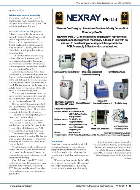
sipation available.<br />
printed electronics versatility<br />
Using ink technology, more <strong>com</strong>plex<br />
circuit boards can be manufactured by<br />
using the more advanced and “green” PEC<br />
technologies described below.<br />
Thermally conductive PEC process<br />
Silk-screen-coating the aluminum with<br />
thermally conductive dielectric, a second<br />
layer of a specially formulated LPI<br />
dielectric ink is deposited at some 1 to<br />
1.2 mil thickness depending on screen<br />
mesh selections. If desired, extra layers<br />
of the dielectric will provide for thicker<br />
conductor lines.<br />
Tack-cured and then exposed using<br />
ordinary UV exposure units, the LPI is<br />
spray developed on typical developing<br />
equipment and chemistry. What remains<br />
is a coating on the substrate with trenches<br />
and pad openings (Figure 5).<br />
A thermally conductive PEC’s third<br />
<strong>com</strong>ponent is a nano technology silver conductive<br />
ink that is applied onto the surface<br />
of the LPI. Filling of the trenches and pads<br />
is ac<strong>com</strong>plished and the conductive ink is<br />
cured. The ink fuses into a solid mass with<br />
a slight deposit on the surface of the LPI,<br />
which is easily removed (Figure 6).<br />
The next step is a repeat of the second,<br />
except that this interconnection layer will<br />
be a via formation layer only. Coat, tack,<br />
expose, develop and silver fill.<br />
Because the LPI is never stripped off<br />
and the entrenched silver conductive ink<br />
is level with the top of the LPI, everything<br />
conductive is flush to the dielectric.<br />
The same process is repeated again for<br />
the second conductive layer.<br />
The result is that the interconnect<br />
“vias” are buried, and there is a 100%<br />
metal connection to the first layer. In the<br />
end, anything reliability-wise to a PCB<br />
PTH interconnect has been eliminated.<br />
The process is repeated for as many<br />
layers as is required by design. The last top<br />
layer has pads left exposed for <strong>com</strong>ponent<br />
mounting. All circuitry and interconnections<br />
are buried.<br />
Versatile, boards can be configured to<br />
use the PEC full additive process even on<br />
two sides of the aluminum if desired or<br />
build multilayer circuits all on one side of<br />
the aluminum backing.<br />
Figure 7 shows a typical PEC build<br />
configuration: A multilayered, single-sided<br />
thermally conductive PEC technology<br />
PCB. Designs could be altered a number<br />
of ways, allowing many new interconnect<br />
possibilities.<br />
www.globalsmtindia.in<br />
conclusion<br />
In summary, using printed electronic ink<br />
products and processes to manufacture<br />
high performance thermally conductive<br />
circuit boards offers clear advantages in<br />
manufacturing flexibility, performance and<br />
cost.<br />
When using these inks in the full additive<br />
print only process or the PEC method,<br />
these high performance heat-dissipating<br />
circuits are also environmentally friendly.<br />
PEC (printed electronic circuit) process for LED interconnection<br />
Mike is an industry veteran going back to<br />
military board manufacturing using shoe eyelets<br />
for interconnection of layers. Joining the ranks<br />
of Caledon Controls, a growing distribution<br />
firm, Mike is involved in diversification efforts<br />
and searching for alternative PCB processing<br />
methods.<br />
Global SMT & Packaging <strong>South</strong>east <strong>Asia</strong> – Winter 2010 – 13