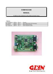
Renesas MCU M16C Family (R32C/M32C/M16C/R8C) - Glyn
Renesas MCU M16C Family (R32C/M32C/M16C/R8C) - Glyn
Renesas MCU M16C Family (R32C/M32C/M16C/R8C) - Glyn

Create successful ePaper yourself
Turn your PDF publications into a flip-book with our unique Google optimized e-Paper software.
Concepts<br />
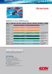
90.00 ><br />
85.00<br />
80.00<br />
75.00 dBuV<br />
70.00<br />
65.00<br />
60.00 ><br />
Low EMI/Excellent EMS<br />
The <strong>M16C</strong> <strong>Family</strong> is designed to maximize EMI/EMS performance. This reduces costs associated with<br />
EMI/EMS countermeasures for application developers.<br />
Low Electromagnetic Interference (EMI)<br />
The <strong>M16C</strong> <strong>Family</strong> is designed to<br />
minimize switching noise. Noise<br />
output is reduced by as much as<br />
20dB.<br />
EM Scan<br />
Measurement method:<br />
EM scan measurement using<br />
electromagnetic field probe<br />
Measurement conditions:<br />
Measurement frequency range<br />
40 to 120MHz<br />
Measuring device: EPS-M1 EM scanner, Noise Laboratory Co., Ltd.<br />
Measurement location: Kansai Electronic Industry Development Center<br />
Measurement frequency range: 30 to 110MHz<br />
Measurement unit: 2mm 2<br />
Power supply: 5 V<br />
Company<br />
<strong>M16C</strong>/62P Clock: 24MHz (PLL) A RISC-A<br />
Excellent Ability to Withstand Noise (EMS)<br />
All <strong>M16C</strong>/<strong>M32C</strong> <strong>MCU</strong>s are<br />
designed using various noise<br />
reduction techniques. These<br />
<strong>MCU</strong>s are extensively tested<br />
using different noise test<br />
methods.<br />
The Vcc and Vss pins are<br />
arranged close together on<br />
<strong>M16C</strong> <strong>MCU</strong>s to prevent noise<br />
from entering via the Vcc and<br />
ground wiring. Internal parasitic<br />
capacitors provide further<br />
protection against noise at the<br />
Vcc and Vss pins. This design<br />
also helps suppress unwanted<br />
noise emission from the chip<br />
itself.<br />
AC 100V<br />
Short Distance between Vcc and Vss<br />
Vcc<br />
GND<br />
3kV<br />
100V<br />
Note noise peaks!<br />
5V<br />
0V<br />
Vcc<br />
GND<br />
(<strong>M16C</strong>)<br />
Power supply: 5 V<br />
Clock: 20MHz (PLL)<br />
Note: Evaluation is also performed using the VDE and TEM cell methods. Only products that meet uniform standards are produced in volume.<br />
Evaluation Method<br />
Noise<br />
Source<br />
Noise Tester<br />
(Spike Noise Generator)<br />
(Conventional)<br />
Noise Propagation<br />
into Chip<br />
5 V Regulator<br />
3-Element Regulator<br />
Noise<br />
Source<br />
Mounting of Decoupling<br />
Capacitor in Optimal Location<br />
1.5kV<br />
EMI/EMS<br />
Evaluation Board<br />
Absorbed as<br />
Common Mode<br />
Noise<br />
Parasitic Capacitor<br />
Line Inductance<br />
12