

Annual Report 2007 - The Australian Nanotechnology Network
Annual Report 2007 - The Australian Nanotechnology Network
Annual Report 2007 - The Australian Nanotechnology Network

You also want an ePaper? Increase the reach of your titles
YUMPU automatically turns print PDFs into web optimized ePapers that Google loves.
optimisation of these nanowires and nanowire heterostructures, and ultimately the success of<br />
nanowire-based optoelectronic devices.<br />
Prior to the visit, I grew a series of GaAs nanowire samples to study (i) the effects of growth<br />
temperature and precursor flow (ii) nanowire doping with Si, Zn and C (iii) the effects of<br />
passivation with an AlGaAs shell and AlGaAs shell composition (iv) quantum confinement<br />
effects within axial quantum wells of GaAs/AlGaAs nanowire superlattices and (v) quantum<br />
confinement within GaAs/AlGaAs quantum well shells.<br />
At UC, I spent many days and late nights in the lab obtaining results whilst ably assisted by UC<br />
PhD students Thang Hoang, Melodie Fickenscher and Saranga Perera. We made several<br />
interesting and important findings. Firstly, time-resolved PL studies revealed a long exciton<br />
lifetime in GaAs nanowires grown at low temperature. This indicates that these low-temperature<br />
grown nanowires have very high optical quality and should find further applications in<br />
optoelectronic devices. Second, we found that intrinsic carbon doping decreases with increasing<br />
arsine precursor flow rate and decreasing temperature, which indicates that highly pure material<br />
can be obtained using high arsine flow rate and low temperature. Also, we obtained some<br />
intriguing results from GaAs/AlGaAs quantum well shell samples which indicate exciton<br />
confinement within quantum well shells. Many of these results will be submitted for publication<br />
very shortly.<br />
Under the guidance of the professors and PhD students at UC, I developed valuable experimental<br />
skills: performing PL characterise my nanowire samples, learning to analyse and interpret the<br />
data, and developing a detailed understanding of the physics of carrier relaxation in<br />
semiconductor nanowires. <strong>The</strong> UC group has great expertise in this area and I gained a much<br />
greater understanding of semiconductor optics. Furthermore, I learnt about the design and<br />
optimisation of such optical characterisation systems. Having returned to ANU, I’m now<br />
applying this knowledge to upgrade and optimise our own laboratory’s existing PL and micro-PL<br />
systems.<br />
Additionally, I presented a seminar to the UC group. This enhanced their understanding of<br />
ANU’s work on nanowire fabrication<br />
and characterisation. I believe that my<br />
visit strengthened collaboration between<br />
our groups, and now we’re in contact on<br />
an almost daily basis.<br />
It was an extremely productive trip. I<br />
worked in a very active and stimulating<br />
research environment, obtained<br />
substantial experimental data and learnt<br />
a great deal. <strong>The</strong> visit was so productive<br />
that I extended the duration of my stay<br />
from one month to two months!<br />
Additionally, I had a fantastic time, met<br />
many wonderful people and made some<br />
lifelong friends. It was fun to experience<br />
life in mid-West America and participate<br />
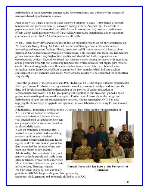
in Halloween, Thanksgiving and Hannah Joyce with her hosts at the University of<br />
Pre-Christmas shopping! I’m extremely Cincinnati<br />
grateful to ARCNN for providing me this opportunity,<br />
and to my kind, generous and extremely skilled hosts at UC.<br />
44
