Chapter 5: Carrier Transport Phenomena - FKE
Chapter 5: Carrier Transport Phenomena - FKE
Chapter 5: Carrier Transport Phenomena - FKE

You also want an ePaper? Increase the reach of your titles
YUMPU automatically turns print PDFs into web optimized ePapers that Google loves.
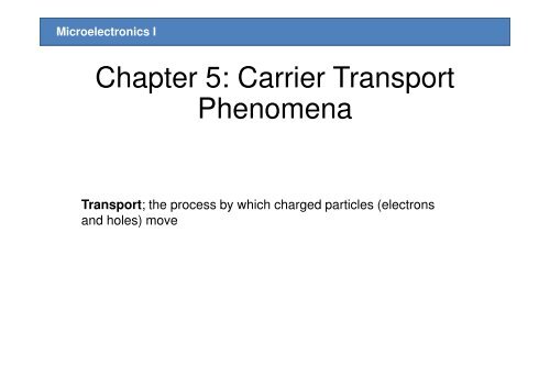
Microelectronics I<br />
<strong>Chapter</strong> 5: <strong>Carrier</strong> <strong>Transport</strong><br />
<strong>Phenomena</strong><br />
<strong>Transport</strong>; the process by which charged particles (electrons<br />
and holes) move
Microelectronics I<br />
Understanding of electrical properties ( I-V characteristics)<br />
Basic current equation;<br />
I ∝ e⋅µ<br />
⋅n⋅<br />
E<br />
e; electronic charged (constant, 1.6 x 10⁻¹⁹ C)<br />
u; mobility ( figure of merit that reflect the speed)<br />
n; carrier concentration<br />
E; Electric field<br />
<strong>Carrier</strong> concentration (electron, n o and hole, p o)<br />
<strong>Chapter</strong> 4<br />
<strong>Carrier</strong> transport (current)<br />
This chapter
Microelectronics I<br />
+<br />
“Drift”<br />
The movement of carrier due<br />
to electric field (E)<br />
E<br />
V<br />
electron<br />
-<br />
<strong>Carrier</strong> <strong>Transport</strong><br />
“Diffusion”<br />
The flow of carrier due to density<br />
gradients (dn/dx)<br />
electron<br />
divider
Microelectronics I<br />
5.1 <strong>Carrier</strong> Drift<br />
Drift current density<br />
Consider a positively charged hole,<br />
When electric field, E, is applied, the hole accelerates<br />
F = mp<br />
a =<br />
*<br />
m*p; effective mass of hole, a; acceleration, e; electronic charge<br />
However, hole collides with ionized impurity atoms and with thermally vibrating<br />
lattice atom<br />
Lattice atom<br />
hole<br />
Ionized impurity atom<br />
eE<br />
E
Microelectronics I<br />
hole<br />
Ionized impurity atom<br />
Holes accelerates<br />
due to E<br />
Involves in collision<br />
(“Scattering Process”)<br />
Loses most of energy<br />
Lattice atom<br />
Gain average drift velocity, v dp<br />
vdp p<br />
= µ E<br />
µ p; Hole mobility (unit; cm 2 /Vs)<br />
Describes how well a carrier move due to E<br />
E
Microelectronics I<br />
Drift current density, J drf (unit; A/cm 2 ) due to hole<br />
J =<br />
p|<br />
drf<br />
epv<br />
J p | drf = p<br />
dp<br />
eµ<br />
pE<br />
Drift current density due to electron<br />
Total drift current;<br />
J n | drf = n<br />
eµ<br />
nE<br />
J drf = n p<br />
e(<br />
µ n + µ p)<br />
E<br />
The sum of the individual electron and hole drift current densities
Microelectronics I<br />
Mobility is important parameter to determine the conductivity of material<br />
Mobility effects<br />
eτ<br />
cp<br />
p *<br />
mp<br />
µ =<br />
µ =<br />
n<br />
eτ<br />
m<br />
τ; mean time between collisions<br />
If τ=10 -15 s, in average, every 10 -15 s, carrier involves in collision @ scattering<br />
Two dominant scattering mechanism<br />
1. Phonon or lattice scattering<br />
2. Ionized scattering<br />
cn<br />
*<br />
n
Microelectronics I<br />
1. Lattice scattering or phonon scattering<br />
At temperature, T > 0 K, atoms randomly vibrate. This thermal vibrations cause a<br />
disruption of the periodic potential function. This resulting in an interaction<br />
between carrier and the vibrating lattice atoms.<br />
Mobility due to lattice scattering, µ L<br />
µ µ<br />
L<br />
∝ T<br />
− 3 / 2<br />
As temperature decreases, the probability of a scattering event decreases. Thus,<br />
mobility increases
Microelectronics I<br />
electron hole
Microelectronics I<br />
2. Ionized Ion scattering<br />
Coulomb interaction between carriers and ionized impurities produces scattering<br />
or collusion. This alter the velocity characteristics of the carriers.<br />
Mobility due to ionized ion scattering, µ I<br />
µ<br />
L<br />
∝<br />
T 2 / 3<br />
N Total ionized impurity concentration<br />
I<br />
If temperature increases, the random thermal velocity of a carrier increases,<br />
reducing the time the carrier spends in the vicinity of the ionized impurity center.<br />
This causes the scattering effect decreases and mobility increases.<br />
If the number of ionized impurity centers increases, then the probability of a<br />
carrier encountering an ionized impurity centers increases, thus reducing<br />
mobility
Microelectronics I
Microelectronics I<br />
The net mobility is given by<br />
1 1<br />
=<br />
µ µ<br />
L<br />
+<br />
1<br />
µ<br />
Due to phonon scattering Due to ionized ion scattering<br />
I
Microelectronics I<br />
Conductivity<br />
Drift current<br />
electron<br />
J drf n p<br />
σ; conductivity [(Ω.cm) -1 ]<br />
= e(<br />
µ n + µ p)<br />
E = σE<br />
hole<br />
σ = ( µ n + µ p)<br />
e n p<br />
Function of electron and hole concentrations and mobolities<br />
Ρ; resistivity [Ω.cm]<br />
1<br />
ρ =<br />
=<br />
σ<br />
1<br />
( µ n + µ p)<br />
e n p
Microelectronics I
Microelectronics I<br />
Current density,<br />
J<br />
I<br />
A<br />
V<br />
Area, A<br />
Bar of semiconductor<br />
L<br />
+<br />
- V<br />
I<br />
V<br />
J = Electric field, E =<br />
A<br />
L<br />
= σE<br />
V<br />
= σ<br />
L<br />
⎛ L ⎞<br />
= ⎜ ⎟I<br />
⎝σA<br />
⎠<br />
⎛ ρL<br />
⎞<br />
= ⎜ ⎟I<br />
⎝ A ⎠<br />
Resistance, R is a function of resistivity, or<br />
conductivity, as well as the geometry of the<br />
semiconductor<br />
=<br />
IR<br />
I
Microelectronics I<br />
Consider p-type semiconductor with an acceptor doping N a (N d=0) in which N a>>n i<br />
Assume complete ionization<br />
σ = ( µ n + µ p)<br />
≈ eµ<br />
p<br />
e n p<br />
n<br />
σ ≈ eµ<br />
nN a<br />
1<br />
≈<br />
ρ<br />
Function of the majority carrier
Microelectronics I<br />
ex.;<br />
Consider compensated n-type Silicon at T=300 K with a conductivity of σ=16<br />
(Ωcm) -1 and an acceptor doping concentration of 10 17 cm -3 . Determine the donor<br />
concentration and the electron mobility.<br />
Solution;<br />
At T=300 K, we can assume complete ionization. (N d-N a >>n i)<br />
σ ≈ eµ<br />
n = eµ<br />
( N<br />
16<br />
=<br />
n<br />
( 1.<br />
6<br />
× 10<br />
n<br />
−19<br />
d<br />
− N<br />
) µ ( N<br />
n<br />
d<br />
a<br />
)<br />
−10<br />
To determine µn and Nd, we can use figure mobility vs. impurity concentration with<br />
trial and error<br />
10<br />
20<br />
= µ<br />
n( Nd<br />
−10<br />
17<br />
)<br />
17<br />
)
Microelectronics I<br />
If N d=2 x 10 17 cm -3 , impurity<br />
concentration, N I= N d + +Na - =3 x 10 17<br />
cm -3 . from the figure, µn= 510<br />
cm 2 /Vs. so σ=8.16 (Ωcm) -1 .<br />
If Nd=5 x 1017 cm-3 , impurity<br />
concentration, NI= N +<br />
d +Na - =6x 1017 cm-3 . from the figure, µn= 325<br />
cm2 /Vs. so σ=20.8 (Ωcm) -1 cm .<br />
2 /Vs. so σ=20.8 (Ωcm) -1 .<br />
N d should be between 2 x 10 17 and 5 x<br />
10 17 cm -3 . after trial and error.<br />
Nd= 3.5 x 10 17 cm -3<br />
µn=400 cm 2 /Vs<br />
σ= 16 (Ωcm) -1
Microelectronics I<br />
Ex 2.; designing a semiconductor resistor with a specified resistance to<br />
handle a given current density<br />
A Si semiconductor at T=300 K is initially doped with donors at a concentration of<br />
N d=5 x 10 15 cm -3 . Acceptors are to be added to form a compensated p-type<br />
material. The resistor is to have a resistance of 10 kΩ and handle a current<br />
density of 50 A/cm 2 when 5 V is applied.<br />
Solution;<br />
When 5 V is applied to 10 kΩ resistor, the current, I<br />
V 5<br />
I = = = 0.<br />
5mA<br />
4<br />
R 10<br />
If the current density, J is limited to 50 A/cm 2 , the cross-sectional area, A is<br />
A =<br />
I<br />
J<br />
=<br />
0.<br />
5×<br />
10<br />
50<br />
−3<br />
= 10<br />
−5<br />
cm<br />
2
Microelectronics I<br />
Consider that electric field, E is limited to 100 V/cm. Then the length of the<br />
resistor, L is<br />
L<br />
V<br />
E<br />
5 −2<br />
= = 5×<br />
10<br />
100<br />
The conductivity, σ of the semiconductor is<br />
=<br />
cm<br />
L<br />
σ = =<br />
cm<br />
RA 10 × 10<br />
−2<br />
5× 10<br />
−1<br />
= 0.<br />
5(<br />
Ω )<br />
4 −5<br />
The conductivity of the compensated p-type semiconductor is<br />
σ ≈ eµ p = eµ<br />
−<br />
p<br />
p ( Na<br />
Nd<br />
Here, the mobility is function of total ionized impurity concentration Na+Nd<br />
)
Microelectronics I<br />
Using trial and error, if Na=1.25x10 16 cm -3 , then Na+Nd=1.75x10 16 cm -3 , and the<br />
hole mobility, from figure mobility versus impurity concentration, is approximately<br />
µp=410 cm 2 /Vs. The conductivity is then,<br />
σ = eµ ( N<br />
p<br />
a<br />
− N<br />
d<br />
)<br />
=<br />
1.<br />
6<br />
× 10<br />
−19<br />
× 410×<br />
(( 12.<br />
5<br />
−<br />
5)<br />
× 10<br />
This is very close to the value we need. From the calculation<br />
L=5x10 -2 cm<br />
A=10 -5 cm 2<br />
Na=1.25x10 16 cm -3<br />
15<br />
)<br />
=<br />
0.<br />
492
Microelectronics I<br />
Velocity Saturation<br />
v d<br />
= µ E<br />
Drift velocity increase linearly with applied electric field.<br />
At low electric field,<br />
vd increase linearly<br />
with applied E.<br />
slope=mobility<br />
At high electric field,<br />
vd saturates<br />
Constant value
Microelectronics I<br />
<strong>Carrier</strong> diffusion<br />
Diffusion; process whereby particles from a region of high concentration toward<br />
a region of low concentration.<br />
Electron concentration, n<br />
<strong>Carrier</strong><br />
Electron flux<br />
divider<br />
Electron diffusion<br />
current density<br />
Position x<br />
J<br />
J<br />
nx|<br />
dif<br />
nx|<br />
dif<br />
⎛ dn ⎞<br />
= ( −e)<br />
Dn⎜<br />
− ⎟<br />
⎝ dx ⎠<br />
dn<br />
= eDn<br />
dx<br />
D n; electron diffusion coefficient
Microelectronics I<br />
Hole centration, p<br />
Hole flux<br />
Hole diffusion<br />
current density<br />
Position x<br />
J<br />
J<br />
px|<br />
dif<br />
px|<br />
dif<br />
=<br />
eD<br />
p<br />
= −eD<br />
⎛<br />
⎜−<br />
⎝<br />
p<br />
dp<br />
dx<br />
dp<br />
dx<br />
D p; hole diffusion coefficient<br />
Diffusion coefficient; indicates how well carrier move as a result of<br />
density gradient.<br />
⎞<br />
⎟<br />
⎠
Microelectronics I<br />
Total Current Density<br />
Electron drift<br />
current<br />
1-D<br />
3-D<br />
Total Current<br />
Density<br />
hole drift<br />
current<br />
Electron diffusion<br />
current<br />
J = J n|<br />
drf + J nx|<br />
dif + J p|<br />
drf + J px|<br />
dif<br />
dn<br />
J = enµ<br />
nE<br />
x + epµ<br />
pE<br />
x + eDn<br />
− eDp<br />
dx<br />
dp<br />
dx<br />
J = enµ<br />
nE<br />
+ epµ<br />
pE<br />
+ eDn∇n<br />
− eDp∇p<br />
hole diffusion<br />
current
Microelectronics I<br />
Mobility,µ; indicates how well carrier moves due to electrical field<br />
Diffusion coefficient, D; how well carrier moves due to density gradient<br />
Here, we derive relationship between mobility and diffusion<br />
coefficient using nonuniformly doped semiconductor model<br />
Graded impurity distribution<br />
electron<br />
“Einstein relation”<br />
x<br />
nonuniformly doped semiconductor<br />
Energy-band diagram<br />
x<br />
E C<br />
E F<br />
E v
Microelectronics I<br />
x<br />
E C<br />
E F<br />
E v<br />
Doping concentration decreases as x increases<br />
Electron diffuse in +x direction<br />
The flow of electron leaves behind positively<br />
charged donor<br />
Induce electrical field, E x, given by<br />
⎛ kT ⎞ 1 dN d ( x )<br />
E Ex<br />
= − ⎜ ⎟<br />
⎝ e ⎠ N ( x)<br />
dx<br />
Since there are no electrical connections, there is no current(J=0)<br />
Electron current<br />
J<br />
=<br />
eµ<br />
N<br />
n<br />
d<br />
dNd<br />
( x)<br />
( x)<br />
Ex<br />
+ eDn<br />
=<br />
dx<br />
0<br />
d<br />
…eq.2<br />
…eq.1
Microelectronics I<br />
From eq.1 and 2,<br />
D<br />
µ<br />
n =<br />
n<br />
kT<br />
e<br />
Hole current must also be zero. We can show that<br />
D<br />
µ<br />
n<br />
Dp kT<br />
=<br />
µ µ e<br />
p<br />
Dp<br />
=<br />
µ<br />
n =<br />
p<br />
kT<br />
e<br />
Diffusion coefficient and mobility are not independent parameters.<br />
The relationship between this 2 parameter “Einstein relation”
Microelectronics I<br />
The Hall effect<br />
Using the effect, we can determine<br />
The type of semiconductor<br />
<strong>Carrier</strong> concentration<br />
mobility<br />
Applied electrical field<br />
Magnetic field<br />
Force on charged particle<br />
in magnetic field (“Lorentz<br />
force”)<br />
F =<br />
qv×<br />
B
Microelectronics I<br />
the Lorentz force on electron<br />
and hole is in –y direction<br />
There will be buildup of negative<br />
charge (n-type) or positive charge<br />
(p-type) at y=0<br />
As a results, an electrical field<br />
called “Hall field, E EH” H” is induced.<br />
Hall field produces “Hall voltage,<br />
V H”<br />
Polarity of V H is used to determine the type of semiconductor<br />
In y-direction, Lorentz force will be balanced by force due to Hall field<br />
qv<br />
V<br />
H<br />
V<br />
B q<br />
W<br />
= v WB<br />
H<br />
x × z = (p-type)<br />
x<br />
z
Microelectronics I<br />
For p-type<br />
For n-type<br />
V<br />
p<br />
H<br />
v<br />
=<br />
x =<br />
I xB<br />
epd<br />
eV H<br />
I x<br />
( ep)(<br />
Wd)<br />
z<br />
I xBz<br />
=<br />
eV d<br />
I xBz<br />
VH<br />
= −<br />
end<br />
I xBz<br />
n = −<br />
eV d<br />
H<br />
Can calculate the hole concentration in p-type<br />
Note that V H is negative for n-type
Microelectronics I<br />
When we know the carrier concentration, we can calculate carrier mobility<br />
J = epµ<br />
E<br />
x<br />
p<br />
x<br />
Similar with n-type, mobility is determined from<br />
n = µ<br />
I xL<br />
enV Wd<br />
x<br />
I epµ<br />
E<br />
x<br />
p<br />
=<br />
Wd L<br />
I xL<br />
µ p =<br />
epV Wd<br />
x<br />
x