

I C™ Serial EEPROM Family Data Sheet - Microchip
I C™ Serial EEPROM Family Data Sheet - Microchip
I C™ Serial EEPROM Family Data Sheet - Microchip

Create successful ePaper yourself
Turn your PDF publications into a flip-book with our unique Google optimized e-Paper software.
3.0 PIN DESCRIPTIONS<br />
The descriptions of the pins are listed in Table 3-1.<br />
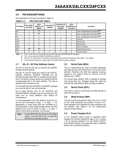
TABLE 3-1: PIN FUNCTION TABLE<br />
Pin Name<br />
8-Pin PDIP<br />
and SOIC<br />
8-Pin<br />
TSSOP and<br />
MSOP<br />
A0 1 1 (1)<br />
5-Pin SOT-23<br />
24XX00<br />
3.1 A0, A1, A2 Chip Address Inputs<br />
The A0, A1 and A2 pins are not used by the 24XX01<br />
through 24XX16 devices.<br />
The A0, A1 and A2 inputs are used by the 24C01C,<br />
24C02C, 24XX014, 24XX024, 24XX025 and the<br />
24XX32 through 24XX1025 for multiple device operations.<br />
The levels on these inputs are compared with the<br />
corresponding bits in the slave address. The chip is<br />
selected if the compare is true.<br />
For the 24XX128 and 24XX256 in the MSOP package<br />
only, pins A0 and A1 are not connected.<br />
Up to eight devices (two for the 24XX128 and<br />
24XX256 MSOP package) may be connected to the<br />
same bus by using different Chip Select bit<br />
combinations.<br />
In most applications, the chip address inputs A0, A1<br />
and A2 are hard-wired to logic ‘0’ or logic ‘1’. For<br />
applications in which these pins are controlled by a<br />
microcontroller or other programmable device, the chip<br />
address pins must be driven to logic ‘0’ or logic ‘1’<br />
before normal device operation can proceed.<br />
24AAXX/24LCXX/24FCXX<br />
5-Pin SOT-23<br />
All except<br />
24XX00<br />
8-Pin<br />
5x6 DFN and<br />
2x3 DFN<br />
3.2 <strong>Serial</strong> <strong>Data</strong> (SDA)<br />
This is a bidirectional pin used to transfer addresses<br />
and data into and out of the device. It is an open drain<br />
terminal. Therefore, the SDA bus requires a pull-up<br />
resistor to VCC (typical 10 kΩ for 100 kHz, 2 kΩ for<br />
400 kHz and 1 MHz).<br />
For normal data transfer, SDA is allowed to change<br />
only during SCL low. Changes during SCL high are<br />
reserved for indicating the Start and Stop conditions.<br />
3.3 <strong>Serial</strong> Clock (SCL)<br />
This input is used to synchronize the data transfer to<br />
and from the device.<br />
3.4 Write-Protect (WP)<br />
This pin must be connected to either VSS or VCC. If tied<br />
to VSS, write operations are enabled. If tied to VCC,<br />
write operations are inhibited but read operations are<br />
not affected. See Table 1-1 for the write-protect<br />
scheme of each device.<br />
3.5 Power Supply (VCC)<br />
Function<br />
— — 1 User configurable Chip Select (3)(4)<br />
A1 2 2 (1) — — 2 User configurable Chip Select (3)(4)<br />
A2 3 3 — — 3 User configurable Chip Select (3)(4)<br />
VSS 4 4 2 2 4 Ground<br />
SDA 5 5 3 3 5 <strong>Serial</strong> <strong>Data</strong><br />
SCL 6 6 1 1 6 <strong>Serial</strong> Clock<br />
(NC) — — 4 — — Not Connected<br />
WP 7 (2)<br />
7 (2)<br />
— 5 7 Write-Protect Input<br />
VCC 8 8 5 4 8 Power Supply<br />
Note 1: Pins 1 and 2 are not connected for the 24XX128 and 24XX256 MSOP packages.<br />
2: Pin 7 is not used for 24XX00, 24XX025 and 24C01C.<br />
3: Pins A0, A1 and A2 are not used by some devices (no internal connections). See Table 1-1 for details.<br />
4: Pin A2 should be tied to a Logic High in the 24XX1025 for proper operation.<br />
Note: In the 24XX1025, the A2 pin is not configurable,<br />
it must be tied to VCC in order for<br />
this device to operate properly.<br />
A VCC threshold detect circuit is employed which<br />
disables the internal erase/write logic if VCC is below<br />
1.5V at nominal conditions. For the 24C00, 24C01C<br />
and 24C02C devices, the erase/write logic is disabled<br />
below 3.8V at nominal conditions.<br />
© 2007 <strong>Microchip</strong> Technology Inc. DS21930C-page 9


