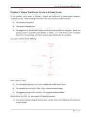
ELET 3132L - Lab #1
ELET 3132L - Lab #1
ELET 3132L - Lab #1

Create successful ePaper yourself
Turn your PDF publications into a flip-book with our unique Google optimized e-Paper software.
<strong>ELET</strong> <strong>3132L</strong> - <strong>Lab</strong> <strong>#1</strong><br />
Logic Gates and Families<br />
Revised 21-August-2010<br />
This exercise has two parts. The first part will be done in the MOSAIC computer lab. Students<br />
will perform simulations using MultiSIM and PSpice. The second part of this exercise will be<br />
done in the regularly scheduled lab room. The report for this exercise will combine the<br />
simulation results and the experimental results.<br />
INTRODUCTION:<br />
This experiment increases the student’s competency with circuit simulation, circuit construction,<br />
power supplies and multimeters. This laboratory also introduces the student to basic combinational<br />
logic gates. Finally this laboratory introduces the student to three digital architectures DTL, TTL and<br />
CMOS.<br />
SIMULATION (Part 1): MultiSim<br />
1. Log into an XP workstation using your username and password.<br />
2. Select Start→All Programs→Mosaic XP→Engineering→EngrTech→MultiSIM.<br />
3. You should see the opening screen from MultiSIM, and messages on the lower border for a<br />
few seconds. Finally you will see a blank schematic screen. First you want to create a place<br />
for the design in your Mosaic space. Select File→Save As, navigate to YOUR workspace (all<br />
the way up to your H drive then make a suitable directory) and type in a name for the project<br />
(I used “DTL”). Your dialog box should look like the one below.<br />
4. Click OK.<br />
Figure 1: SAVE AS Dialog Box<br />
5. First you will place components on your schematic (we’ll wire them later). A screen shot of<br />
the completed schematic for this first simulation appears below to help you can decide where<br />
to place parts.<br />
<strong>ELET</strong> <strong>3132L</strong> Experiment <strong>#1</strong> 1 of 25
Figure 2: Multisim Screen Shot<br />
6. From the top bar menu select Place→Component… to open the component placement dialog<br />
box.<br />
7. This dialog box has several levels. Always use the Master Database – this database has all<br />
the parts you will need for your schematics. First choose the type of component you wish to<br />
place from the second drop down menu on the left. Then choose the specific component from<br />
the list on the right. For starters, pick Transistors from the second drop down menu on the<br />
left then pick BJT_NPN from the list of transistor types. Now find 2N3904 in the right side<br />
list of specific parts. Highlight 2N3904 as shown below then click OK.<br />
<strong>ELET</strong> <strong>3132L</strong> Experiment <strong>#1</strong> 2 of 25
Figure 3: Component Selection Dialog Box<br />
8. Place the transistor on your blank schematic page. Now you will place the diodes on your<br />
schematic. Select Place→Component… again then from the lower left drop down menu<br />
choose Diodes. Select 1N914 from the column on the right and click OK. Place the diodes<br />
on the schematic.<br />
9. Notice the orientation is not correct for all of the diodes. To change the orientation on a diode<br />
(or any other component), put the cursor over the diode (component) and left-click once to<br />
select the diode (component). Then right-click once to open the operations menu for the<br />
selected component (see below). Select Flip Horizontal to spin the diode around.<br />
Figure 4: Pop-Up Menu<br />
<strong>ELET</strong> <strong>3132L</strong> Experiment <strong>#1</strong> 3 of 25
10. Other useful operations on this menu include Properties (this is how you change the voltage<br />
on a battery or the frequency of a clock), Cut Copy Paste Delete can be used to copy selected<br />
components (saves time from having to go all the way through the menu system) and Font<br />
can be used to alter the size and appearance of text associated with the component.<br />
11. After flipping the two diodes on the left, add the two resistors. Resistors are in the Basic<br />
component group. Notice when you select RESISTOR there are two more drop down menus<br />
at the top of the dialog box – one is labeled Filter and is used to show either ALL, Ω, kΩ, or<br />
MΩ. You need to place a 4.7kΩ resistor so choose kΩ. The other drop down is for tolerance<br />
– the default of 5% is fine for digital work. Put the two resistors on the schematic and rotate<br />
them correctly.<br />
12. Now you need a power source. Choose Place →Component… again then select Sources and<br />
DC_Power to get a battery. Place it on the schematic then use the Properties item to change<br />
the voltage from 12 to 5. (You can also double left click on 12 then type in 5 and Enter.)<br />
13. Now you need to add two inputs to your circuit. In real life you could use switches but for<br />
simulation we will hook up two clocks – one for each input – and run them at different<br />
frequencies. That way we will generate all possible input patterns quickly. Choose<br />
Place→Component… then Sources→SIGNAL_VOLTAGE→CLOCK_VOLTAGE to place<br />
a clock generator. Add a second clock generator so you have one for each input.<br />
14. You must change the frequency on one of the clock generators. You could left click then<br />
right click then select Properties like you did with the battery. But there is a faster way. Just<br />
double left click on the text you want to change – in this case the leftmost one. So put the<br />
cursor arrow on top of the 1kHz frequency for the leftmost clock generator and double left<br />
click. Type in 2 in the dialog box and click OK. At this point your schematic should look<br />
something like:<br />
Figure 5: Component Placement<br />
<strong>ELET</strong> <strong>3132L</strong> Experiment <strong>#1</strong> 4 of 25
15. Now you can add wires to connect the components. MultiSIM makes placing wires very<br />
simple though it is a little tricky. First put the cursor exactly over the end of a component.<br />
The cursor will become a dot. Left click once – this establishes the start point for the wire.<br />
Now move the cursor and watch the wire being drawn. At any point you can left-click once<br />
to force the wire to follow a particular shape – else EWB will only allow two bends in the<br />
wire. The wire is completed when you left click on the connection at another component or<br />
when you left click over another wire or when you double left-click.<br />
16. Finally you need to place grounds - under Sources→POWER_SOURCES→Ground. Place<br />
grounds on the schematic at the negative batter terminal, the negative clock generator<br />
terminals and the emitter of the transistor.<br />
17. Before you simulate, you will add net names. EWB gives every wire on your drawing a<br />
name. Wires that are connected together have the same name. These names are called net<br />
names. You can change the net name by double left-clicking on a wire in the net then typing<br />
in the new net name followed by the Enter key. Change the names on the nets we want to<br />
see from simulation – the two inputs and the output of your logic gate.<br />
18. Change the name of the net containing the positive terminal of the leftmost clock generator to<br />
INA. Change the name of the net containing the positive terminal of the other clock<br />
generator to INB. Change the name of the net containing the collector of the transistor to<br />
OUTY. Now you schematic should appear as below:<br />
Figure 6: Finished Schematic<br />
19. You are now ready to simulate. We will use a transient analysis as shown below:<br />
<strong>ELET</strong> <strong>3132L</strong> Experiment <strong>#1</strong> 5 of 25
Figure 7:Simulate Menu<br />
20. There are only two things to setup. First set the stop time to 2 milliseconds so you can see<br />
two complete cycles of the slowest input (1kHz). Do this by changing TSTOP to 0.002.<br />
21. Second you need to pick what voltages to see on the output plot. Choose the Output tab then<br />
use the Add and Remove buttons to make your output display dialog box look like the one<br />
below.<br />
Figure 8: Transient Analysis<br />
<strong>ELET</strong> <strong>3132L</strong> Experiment <strong>#1</strong> 6 of 25
22. Left-click the Simulate button to run the simulation. Your output plot probably looks a little<br />
confusing (Figure 9). That’s OK – we’ll unscramble it in a minute – but first notice all three<br />
voltages (INA, INB, OUTY) are overlaid on the same plot. All voltages are either 0 or 5<br />
volts as expected. There is some noise on the output at the switching times.<br />
Figure 9: Results Window<br />
23. There is a fast way to see all the traces individually. You will loose the voltage information<br />
because the vertical scale will get scrambled. Right click once inside the plot and select<br />
Properties. You will get a dialog box as shown:<br />
Figure 10: Graph Properties Dialog Box<br />
<strong>ELET</strong> <strong>3132L</strong> Experiment <strong>#1</strong> 7 of 25
24. Left click once on Auto-Separate then left click once on Apply then left click once on OK.<br />
You may also want to make your plot window larger and reverse the background. Your plot<br />
should now look like:<br />
Figure 11: All Traces<br />
25. Choose File→Print to print the plot for your lab report. Close the plot window. Choose<br />
File→Print to print the schematic for your lab report. Choose File→Save All to save the<br />
entire DTL project in case you want to refer to it later. Close MultiSIM for now.<br />
SIMULATION (Part 2): PSpice<br />
1. Now you will perform a similar simulation using PSpice. To start PSpice, select Start→All<br />
Programs→MosaicXP→Engineering→Electrical→Cadence PSpice→Capture CIS. It can<br />
take a half-minute or so to start (depends on how busy the MOSAIC network is). Eventually<br />
you will see a dialog box as Capture starts. Pick the PCB Design Studio with Capture CIS<br />
choice. Capture CIS is the schematic entry point to PSpice.<br />
Figure 12: Suite Selection<br />
<strong>ELET</strong> <strong>3132L</strong> Experiment <strong>#1</strong> 8 of 25
2. When Capture starts, you will see a blank project. Choose File→New→Project to make a<br />
new project. You will see the following dialog box. Make sure you pick a directory on your<br />
H drive, choose Analog or Mixed A/D and type in a name for your project (I used CMOS).<br />
Figure 13: New Project Dialog Box<br />
3. PAY ATTENTION: THIS IS IMPORTANT!! Capture is used for many different things<br />
from schematics to board design to simulation work. As such, it has many different parts<br />
libraries. You MUST use parts libraries that have PSpice simulation parameters. You will set<br />
the libraries up first so you have only PSpice parts in your design.<br />
4. Similar to MultiSIM, select Place→Part from the top menu bar. This is where part libraries<br />
are specified for Capture. You will see a dialog box as shown below. The first thing to do is<br />
to remove all the “unPSpice” parts libraries. So select each library by left clicking once on it<br />
then left click on the Remove Library button to remove it. You cannot remove the Design<br />
Cache – that is a file used to cache parts for your design. When you have finished removing<br />
libraries the dialog box should look like Figure 14:<br />
Figure 14: PLACE PART Dialog Box<br />
<strong>ELET</strong> <strong>3132L</strong> Experiment <strong>#1</strong> 9 of 25
5. Now you will need to add the appropriate PSpice libraries to your project. From this same<br />
dialog box, left click the Add Library button. You will see a new dialog box showing all the<br />
libraries at the current location. Browse to the PSpice directory as shown:<br />
Figure 15: Open Dialog Box<br />
6. From the PSice directory, add the following libraries: analog.olb (contains miscellaneous<br />
passive parts), pwrmos.olb (contains MOSFET’s) and source.olb (contains power supplies<br />
and signal generators). When you finish your Place Parts dialog box should look like the one<br />
below.<br />
Figure 16: Part Selection Dialog Box<br />
7. Below (Figure 17) is a completed sketch of the schematic you will make. This should help<br />
you decide where to place items.<br />
<strong>ELET</strong> <strong>3132L</strong> Experiment <strong>#1</strong> 10 of 25
Figure 17: Completed Schematic<br />
8. You are now ready to start placing parts. First place the P channel MOSFETs used to make<br />
this gate. Left click once on the PWRMOS library then type IRF9530 in the Part window.<br />
Capture will show you a complete part number IRF9530 and preview the part in the window.<br />
Click OK to place this part. Drop one on the schematic by left clicking once where you want<br />
the transistor. Place another one under the first one as shown in the example above. Since<br />
you only need two of them, press the Esc key to quit placing parts. These parts are P channel<br />
MOSFETs. As you may have noticed they are “upside down” for our purposes – the drain is<br />
on the top and the source is on the bottom. The procedure for flipping them is similar to that<br />
in ModelSIM; select a part by left-clicking on it. Then rightclick to get an operations menu as<br />
shown below (Figure 18). Choose Mirror Vertically to flip the part vertically. Notice this is<br />
also how you Copy, Edit Properties, etc.<br />
Figure 18: Pop Up Menu<br />
<strong>ELET</strong> <strong>3132L</strong> Experiment <strong>#1</strong> 11 of 25
9. Now you can place the complementary parts – N channel MOSFETs. Use the same methods<br />
to place two of the IRF530 N channel MOSFETs on the schematic. These four transistors are<br />
all the parts needed for the logic gate. But as before you need to add a battery for power, two<br />
signal generators and ground connections.<br />
10. Choose Place→Parts again and select the SOURCE library. Add a battery by adding a VDC<br />
part to the schematic. Left click twice on the 0VDC and change it to 5V. Add the signal<br />
generators by adding two VPWL (Piece-Wise Linear) parts to the schematic. These are<br />
tougher to setup as you will have to describe the signal you want as pieces of lines. Be<br />
careful to setup the times and volts correctly. Left click twice on the top left signal generator.<br />
You will see the property editor screen as shown below.<br />
Figure 19: Property Editor Screen<br />
11. Figure 20 shows a single line of properties for the part. Use the scroll bar at the bottom to<br />
scroll far enough to the right to bring up the Time and Voltage slots as shown below:<br />
Figure 20: Single Line of properties<br />
12. Here is how to setup the signal generator. V1 is the voltage the generator will output at time<br />
T1, V2 at T2, V3 at T3, etc. YOU MUST ADD UNITS – s for seconds and v for volts. Here<br />
are the T’s and V’s to make a 500Hz square wave:<br />
<strong>ELET</strong> <strong>3132L</strong> Experiment <strong>#1</strong> 12 of 25
Figure 21: Values for the Signal Generator<br />
13. When you finish putting in all eight times and voltages, be sure to left click once on the<br />
Apply button to save your work on this signal generator. You will see a little dialog box<br />
warning you that you are about to change something. Left click YES to proceed with saving<br />
your signal generation info.<br />
Figure 22: Warning Dialog Box<br />
14. Next left click on the lower X (see below) to kill the properties window (the upper X kills<br />
Capture). Ignore the error message and click NO when asked to save somewhere else.<br />
Figure 23: Choose the lower X<br />
15. Setup the right most signal generator in the same way. Left click twice on it. Then scroll all<br />
the way to the right of the properties line. This setup is shorter – you only need to enter 4<br />
pairs of numbers as shown in the table below. Remember to type in units also.<br />
<strong>ELET</strong> <strong>3132L</strong> Experiment <strong>#1</strong> 13 of 25
Figure 24: Signal Generator Properties<br />
16. Be sure to left click the Apply button and left click Yes in the dialog box when you finish.<br />
Then close the properties window (the lower X), ignore the error dialog box and click on NO<br />
to avoid saving somewhere else.<br />
17. Left click once on the wiring tool in the right hand tool bar (see below) to wire the parts<br />
together. Similar to MultiSIM, you start wiring by left clicking once. You stop wiring by leftclicking<br />
twice. You stop placing wires by pressing the Esc key.<br />
Figure 25: Wiring Tool<br />
18. The final step is to add net names to the nets you want to see in the simulation output.<br />
Choose the net name tool from the right hand tool bar as shown below. Type in the net name<br />
INA followed by the Enter key for the leftmost signal input. Place the net name on the INA<br />
wire above the VPWL and left click. Press Esc to end placing that net name.<br />
Figure 26: Net Names Tool<br />
19. Repeat the previous step to add the name INB to the rightmost signal generator input.<br />
20. Repeat to add the name OUTY to the output connection between the P channel and N channel<br />
transistor drains.<br />
<strong>ELET</strong> <strong>3132L</strong> Experiment <strong>#1</strong> 14 of 25
Figure 27: Placing Ground<br />
21. For the final step in preparing the schematic, add grounds to the battery, signal generators<br />
and source leads of the N channel transistors. PAY ATTENTION: THIS IS<br />
IMPORTANT!! You must use a particular ground (the 0/SOURCE ground) in order for<br />
your simulations to work. To find this ground, choose the ground tool from the right hand<br />
tool bar as shown below. Then select the entry called 0/SOURCE as shown below. Place<br />
grounds as needed in the circuit.<br />
22. Select PSpice→New Simulation Profile to create a profile describing how want this<br />
schematic simulated. You will see a dialog box like the one below. Be sure to set the<br />
Analysis Type to Time Domain (Transient) and the Run to time to 4000us (4000 micro<br />
seconds is 0.004 seconds – the end of the PWL data):<br />
Figure 28: Simulation Dialog Box<br />
23. Left click OK to accept your changes and close the dialog box.<br />
24. Select PSpice→Run from the top menu bar to run the simulation. This may take a few<br />
seconds. When it completes you will see a message in the simulation message window<br />
saying “Simulation complete”. Then PSpice will open an empty trace window. To add<br />
traces to the window, select Trace→Add Trace from the top menu bar. You will see the Add<br />
Traces dialog box as shown below. Unclick all of the middle boxes except Analog and<br />
Voltages as shown below. Then left click once on V(INA) to add that trace to the plot. Click<br />
OK to close the dialog box for now.<br />
<strong>ELET</strong> <strong>3132L</strong> Experiment <strong>#1</strong> 15 of 25
Figure 29: Add Traces Dialog Box<br />
25. Now your plot window should look like the one below (Figure 30) with a single trace in it.<br />
Figure 30: Trace Results Window<br />
26. You will add two more plots to the window and put INB in the second plot and OUTY in the<br />
third plot. From the top menu bar select Plot→Add Plot to Window as shown below. This<br />
will add a second plot to the window.<br />
<strong>ELET</strong> <strong>3132L</strong> Experiment <strong>#1</strong> 16 of 25
Figure 31: Plot Menu<br />
27. Now repeat the procedure in step 50 to add V(INB) to this plot. Then repeat step 51 to add<br />
another plot and repeat step 50 to add V(OUTY) to that plot. Your trace window should now<br />
look like the one shown below.<br />
Figure 32: Trace Results with new Traces<br />
28. The PSpice program has scaled the top plot differently from the first two, probably because<br />
the voltage spikes a bit above 5 and a bit below ground. You can change the scaling by<br />
selecting Plot→Axis Settings from the top menu bar. Then select the Y-Axis and select the<br />
User Defined radio button. Type in the new scale values of -1V for the lower limit and 6V<br />
for the upper limit and click OK. Change the scales on the other plots as well – this will<br />
make them much easier to read on a printout. (Else the plot and grid cover each other.)<br />
29. Notice if you try to print this plot on a black and white printer, you will not be able to see the<br />
actual data trace for all the grid lines. You will need to turn off the grid lines before printing<br />
your traces. As before, select Plot→Axis Settings. Then select the X Grid tab. Now select<br />
the radio buttons by None on both the Major and Minor grid configurations as shown in<br />
Figure 32:<br />
<strong>ELET</strong> <strong>3132L</strong> Experiment <strong>#1</strong> 17 of 25
Figure 33: Axis Settings Dialog Box<br />
30. This turns off the X grid for all plots. The Y grid must be turned off on each plot. Select a<br />
plot by left clicking in it then disable the Y grid for it. Repeat for all three. Now your plot<br />
window should look like:<br />
Figure 34: PSpice Results<br />
31. Capture this image for your lab report. Open Microsoft Paint and place this image in Paint.<br />
Choose Image→Invert Colors to make this image presentable for your lab report (see Figure<br />
35).<br />
<strong>ELET</strong> <strong>3132L</strong> Experiment <strong>#1</strong> 18 of 25
Figure 35: Inverted Colors (Using Paint)<br />
32. Select File→Save in the Capture main window. Select File->Print to print your schematic for<br />
your lab report. Then close Capture.<br />
SIMULATION (Part 3): Circuit 3: Your Choice: PSpice or MultiSim<br />
1. For the final simulation, you choose whether you want to use PSpice or MultiSIM. Print your<br />
schematic and simulation for your lab report. Remember the steps:<br />
• Sart the appropriate program<br />
• Use SaveAs to name your simulation and store it in an appropriate directory<br />
• Draw the schematic<br />
• Setup the simulation<br />
• Run the simulation<br />
2. Here is the schematic for part 3 in MultiSIM and in PSpice format:<br />
<strong>ELET</strong> <strong>3132L</strong> Experiment <strong>#1</strong> 19 of 25
Figure 36: Circuit 3 in MultiSim<br />
Figure 37: Circuit 3 in PSpice<br />
<strong>ELET</strong> <strong>3132L</strong> Experiment <strong>#1</strong> 20 of 25
Logic Gates and Families<br />
You will build the three logic circuits that you simulated on the computer. You will replace the<br />
signal generators used as inputs in the simulations with switches in the lab. You will also need<br />
pull-up resistors for the CMOS circuit inputs.<br />
INTRODUCTION:<br />
This laboratory increases the student’s competency with circuit simulation, circuit construction,<br />
power supplies, multimeters and oscilloscopes. This laboratory also introduces the student to basic<br />
combinational logic gates. Finally this laboratory introduces the student to three digital architectures<br />
DTL, TTL and CMOS.<br />
EQUIPMENT AND COMPONENTS:<br />
1 - dual trace oscilloscope<br />
1 - function generator<br />
1 - digital multimeter battery powered or isolated<br />
1 - power supply +5 volt<br />
2 - bipolar junction transistor 2N3904<br />
3 - diode 1N914<br />
1 - P channel IRF9530<br />
1 - N channel IRF530<br />
2 - resistor 4.7K, ¼W<br />
2 - switch SPST<br />
<strong>ELET</strong> <strong>3132L</strong> Experiment <strong>#1</strong> 21 of 25
PROCEDURE:<br />
Steps 1 through 3: typical TTL (Transistor-Transistor Logic) Gate<br />
Figure 38: TTL Logic Gate<br />
Step 1. Construct the circuit shown in Figure 38 above with the +5V supply off and the function<br />
generator off. Turn the function generator amplitude all the way down.<br />
Step 2. Turn on the +5V supply. Turn on the function generator and set it for a sine wave, 1kHz,<br />
5VP-P with a 2.5VDC offset (0 to 5V signal). Use the oscilloscope to determine at what<br />
input voltage the Q1 turns on (VOUT = 0) and at what input voltage Q1 turns OFF<br />
(VOUT = 5V).<br />
Step 3. Fill out Table 1 as required.<br />
NM V V<br />
Table 1: Noise Margins<br />
= − LO<br />
Lo HI OUTHI INHI<br />
LO IN OUT<br />
NM = V − V<br />
What logic function does this TTL gate implement?__________________________<br />
<strong>ELET</strong> <strong>3132L</strong> Experiment <strong>#1</strong> 22 of 25
Steps 4 through 6: typical DTL (Diode-Transistor Logic) logic gate<br />
Figure 39: DTL Logic Gate<br />
Step 4. Construct the circuit shown in Figure 39 above with the +5V supply off.<br />
Step 5. Attach the multimeter between the collector of Q1 (plus lead) and ground (minus lead).<br />
Set the multimeter to read Volts DC.<br />
Step 6. Turn on the +5V supply. Measure the output voltage at Q1 for each of the four possible<br />
input conditions. Fill in Table 2 below.<br />
Table 2: Truth Table for the DTL Circuit<br />
What logic function does this DTL gate implement?_________________________<br />
<strong>ELET</strong> <strong>3132L</strong> Experiment <strong>#1</strong> 23 of 25
Steps 7 through 9: typical CMOS (Complementary Metal Oxide Semiconductor) logic gate<br />
Figure 40: CMOS Logic Gate<br />
Step 7. Construct the circuit shown in Figure 40 above with the +5V supply off..<br />
Step 8. Attach the multimeter between the gate output where Q2, Q3 and Q4 drains are all tied<br />
together (plus lead) and ground (minus lead). Set the multimeter to read Volts DC.<br />
Step 9. Turn on the +5V supply. Measure the output voltage at Q3 drain for each of the four<br />
possible input conditions. Fill in Table 3 below.<br />
Table 3: Truth Table for CMOS Circuit<br />
What logic function does this CMOS gate implement?________________________<br />
<strong>ELET</strong> <strong>3132L</strong> Experiment <strong>#1</strong> 24 of 25
QUESTIONS:<br />
1. How does your lab data compare with your simulation results for each of the three circuits?<br />
2. Are the noise margins on the TTL inverter symmetric? Why or why not?<br />
3. Some DTL and TTL logic gates were manufactured with Open Collector outputs (no internal<br />
pull-up resistor on the collector of the output transistor). Why were pull-ups not necessary<br />
with TTL? (Hint: What is the default state of a TTL input if nothing is connected to it?)<br />
4. The gate on a MOSFET transistor requires almost no current. If the inputs are not driven<br />
either high or low then CMOS logic gates drift unpredictably causing erratic operation and<br />
excessive current consumption. Why are pull-up resistors required when interfacing open<br />
collector devices to CMOS logic gates?<br />
5. The DTL gate will draw about 2 mA when no input is supplied (5V / 4.7KΩ ≈ 1mA). About<br />
how much will the TTL gate draw? About how much will the CMOS gate draw? Which logic<br />
family (DTL, TTL, CMOS) do you think uses less power? Why?<br />
Signatures (turn this sheet in with your lab report):<br />
DTL Gate Simulation:<br />
___________________________________________________________________<br />
(Instructor Signoff)<br />
TTL Gate Simulation:<br />
___________________________________________________________________<br />
(Instructor Signoff)<br />
CMOS Gate Simulation:<br />
___________________________________________________________________<br />
(Instructor Signoff)<br />
TTL Inverter Built:<br />
___________________________________________________________________<br />
(Instructor Signoff)<br />
DTL Gate Built:<br />
___________________________________________________________________<br />
(Instructor Signoff)<br />
CMOS Gate Built:<br />
___________________________________________________________________<br />
(Instructor Signoff)<br />
<strong>ELET</strong> <strong>3132L</strong> Experiment <strong>#1</strong> 25 of 25