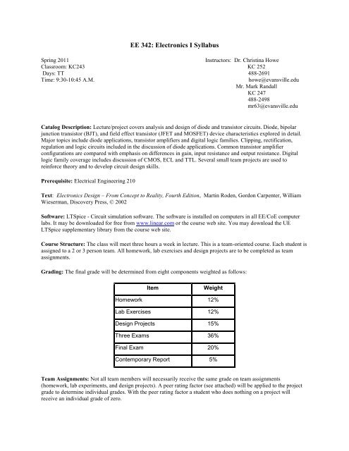
EE 342: Electronics I Syllabus - csserver
EE 342: Electronics I Syllabus - csserver
EE 342: Electronics I Syllabus - csserver

Create successful ePaper yourself
Turn your PDF publications into a flip-book with our unique Google optimized e-Paper software.
<strong>EE</strong> <strong>342</strong>: <strong>Electronics</strong> I <strong>Syllabus</strong><br />
Spring 2011 Instructors: Dr. Christina Howe<br />
Classroom: KC243 KC 252<br />
Days: TT 488-2691<br />
Time: 9:30-10:45 A.M. howe@evansville.edu<br />
Mr. Mark Randall<br />
KC 247<br />
488-2498<br />
mr63@evansville.edu<br />
Catalog Description: Lecture/project covers analysis and design of diode and transistor circuits. Diode, bipolar<br />
junction transistor (BJT), and field effect transistor (JFET and MOSFET) device characteristics explored in detail.<br />
Major topics include diode applications, transistor amplifiers and digital logic families. Clipping, rectification,<br />
regulation and logic circuits included in the discussion of diode applications. Common transistor amplifier<br />
configurations are compared with emphasis on differences in gain, input resistance and output resistance. Digital<br />
logic family coverage includes discussion of CMOS, ECL and TTL. Several small team projects are used to<br />
reinforce theory and to develop circuit design skills.<br />
Prerequisite: Electrical Engineering 210<br />
Text: <strong>Electronics</strong> Design – From Concept to Reality, Fourth Edition, Martin Roden, Gordon Carpenter, William<br />
Wieserman, Discovery Press, © 2002<br />
Software: LTSpice - Circuit simulation software. The software is installed on computers in all <strong>EE</strong>/CoE computer<br />
labs. It may be downloaded for free from www.linear.com or the course web site. You may download the UE<br />
LTSpice supplementary library from the course web site.<br />
Course Structure: The class will meet three hours a week in lecture. This is a team-oriented course. Each student is<br />
assigned to a 2 or 3 person team. All homework, lab exercises and design projects are to be completed as team<br />
assignments.<br />
Grading: The final grade will be determined from eight components weighted as follows:<br />
Item Weight<br />
Homework 12%<br />
Lab Exercises 12%<br />
Design Projects 15%<br />
Three Exams 36%<br />
Final Exam 20%<br />
Contemporary Report 5%<br />
Team Assignments: Not all team members will necessarily receive the same grade on team assignments<br />
(homework, lab experiments, and design projects). A peer rating factor (see attached) will be applied to the project<br />
grade to determine individual grades. With the peer rating factor a student who does nothing on a project will<br />
receive an individual grade of zero.
Homework: Typically, two to five homework problems will be assigned every class period. Three or four class<br />
assignments will be grouped into a homework set and homework sets will be collected on an approximately weekly<br />
basis. To succeed in this course it is critically important that all homework problems be completed. Only one<br />
homework solution is to be turned in per team and every student on the team should understand each problem<br />
solution. Each homework solution should be signed by all team members. Each team may develop their own method<br />
for producing the homework solution, but division-of-work methods (one team member works one problem, a second<br />
team member works another problem, etc.) are not allowed. (One method that works well is to designate one person<br />
as the recorder while other team members brainstorm on solutions to the problem. A different person acts as<br />
recorder for each problem.) A Peer Rating Factor method will be used to determine individual grades on homework<br />
assignments. (Refer to the Team Projects paragraph above.)<br />
Lab Exercises: The lab exercises will be performed outside of class. Lab exercises are designed to take<br />
approximately one hour to complete. The lab exercise write-up only need contain the results of the exercise and a<br />
brief discussion of the results. Only one lab exercise write-up is to be handed in per team. The write-up should be<br />
done on a word processor. All graphs should be of professional quality (generated by a spreadsheet program or other<br />
computer plotting program). In lab exercises requiring both physical and simulated measurements the team may<br />
divide into groups, with one group recording the physical measurements while the other group does the simulation.<br />
Students must rotate the tasks of circuit construction, circuit verification, measurement, and data recording (one<br />
student may be responsible for more than one task) from one exercise to the next. Each lab exercise write-up should<br />
be signed by all team members. A Peer Rating Factor method will be used to determine individual grades on lab<br />
exercises. (Refer to the Team Projects paragraph above.)<br />
Design Projects: There will be two to three design projects during the semester. Design projects are open-ended and<br />
are more time consuming than lab exercises. A design project report is more comprehensive than a lab exercise<br />
write-up. Only one project report is to be written per team. Each project report should be signed by all team<br />
members. A Peer Rating Factor method will be used to determine individual grades on design projects. (Refer to the<br />
Team Projects paragraph above.)<br />
Exams: Three exams will be given during the normal class meeting time.<br />
Final Exam: Approximately one-third of the final exam will be over material covered after the third regular exam,<br />
the other two-thirds of the exam will be comprehensive.<br />
Contemporary Report: This is a summary report about new engineering technology or a current issue affecting the<br />
engineering profession. Sources of information include the Internet, professional society meetings, or technical or<br />
professional magazines.<br />
Reading Assignments: Reading assignments will be given every class period. All reading assignments should be<br />
completed before the next class period.<br />
Attendance: Regular attendance is critical to your success in this course. Please refer to the section on Class<br />
Attendance in the student handbook.<br />
Class Policies: Students are expected to abide by the Academic Honor Code. No aid should be given or requested<br />
on any examination. Students may collaborate on homework (in fact, this is encouraged), but each student must<br />
submit their own work. Each student is expected to be able to recreate any homework solutions submitted. Students<br />
working on team projects are expected to participate in all aspects of the project. Each student on a project team<br />
should do their fair share of the work. Collaboration between project teams is not permitted.<br />
Topics:<br />
Semiconductor materials and properties<br />
Diode characteristics and circuits<br />
Bipolar junction transistors (BJTs)<br />
Field-effect transistors (FETs)<br />
Small Signal Transistor Models<br />
Single Stage Transistor Amplifiers<br />
Bipolar digital circuits. (TTL, ECL)<br />
MOSFET digital circuits. (CMOS)
Course Objectives<br />
List characteristics of semiconductor material.<br />
Understand diode structure and various diode models.<br />
Apply various diode models in circuit analysis.<br />
Design diode rectifiers and wave-shaping circuits.<br />
Design DC power supplies.<br />
Understand the operation of bipolar junction transistors (BJTs).<br />
Analyze BJT biasing circuits by employing an appropriate model for the BJT.<br />
Understand the operation of field-effect transistors (FETs).<br />
Analyze FET biasing circuits by employing an appropriate model for the FET.<br />
Employ small-signal models in the analysis of transistor amplifiers.<br />
Calculate the voltage gain and input and output resistances of transistor amplifier circuits.<br />
Analyze and design common single stage transistor amplifiers.<br />
Analyze CMOS, ECL and TTL logic gates.<br />
University Objectives<br />
Students will acquire a depth of knowledge in one or more disciplines of their choice.<br />
Students will master communication, organizational and critical thinking skills.<br />
Students will develop skills and competencies to be productive team members and leaders.<br />
Students will seek and use available resources, including technology, to answer questions and solve<br />
problems.
Lecture Schedule:<br />
This schedule is tentative. The instructor reserves the right to change it.<br />
Tuesday Thursday<br />
Jan. 11 Jan. 13<br />
Ch. 1 & 3.0-3.1 3.2<br />
Intro & Semiconductor Physics Semiconductor Diodes<br />
Jan. 18 Jan. 20<br />
3.3-3.4 3.5, 3.7<br />
Rectification and Zener Diodes Clippers, Clampers, Other Diodes<br />
Jan. 25 Jan. 27<br />
3.8 / Review Exam I - Ch 1 & 3<br />
Manufacturers' Specs<br />
Feb. 1 Feb. 3<br />
4.0-4.3 4.4-4.8<br />
BJT Structure and Models AC Model, Response Curves, Amp Biasing<br />
Feb. 8 Feb. 10<br />
4.9-4.11 4.12-4.15<br />
BJT Biasing, Power, and Amp Analysis BJT Analysis and Design<br />
Feb. 15 Feb. 17<br />
5.1-5.2 5.3-5.4<br />
CE and ER Amplifiers EF and CB Amplifiers<br />
Feb. 22 Feb. 24<br />
5.5-5.8 5.9 / Review<br />
Applications and Coupling Cascode Configuration<br />
Mar. 1 Mar. 3<br />
Exam II - Ch 4 & 5 6.0-6.3<br />
MOSFETs and JFETs<br />
Mar. 8 Mar. 10<br />
NO CLASS NO CLASS<br />
SPRING BREAK SPRING BREAK<br />
Mar. 15 Mar. 17<br />
6.4-6.5 6.6-6.9<br />
FET Amplifier Configurations and Ics FET Amplifier Analysis<br />
Mar. 22 Mar. 24<br />
6.10 14.0-14.2<br />
FET Amp Design High-Pass RC and Lo-Pass RC Networks<br />
Mar. 29 Mar. 31<br />
14.3-14.5 14.5 / Review<br />
Diodes, Trigger Circuits, 555 Timer 555 Timer<br />
Apr. 5 Apr. 7<br />
Exam III - Ch 6 & 14 15.0-15.4<br />
Basics of Digital Logic and Digital BJTs<br />
Apr. 12 Apr. 14<br />
15.5-15.6 15.7-15.9<br />
Logic Families and TTL ECL and Digital FETs<br />
Apr. 19 Apr. 21<br />
15.10-15.11 Open<br />
CMOS<br />
Apr. 26<br />
Final Review<br />
The Final Exam is on Wednesday, May 4th at 10:15 AM