MB9A110 Series - Fujitsu
MB9A110 Series - Fujitsu
MB9A110 Series - Fujitsu

You also want an ePaper? Increase the reach of your titles
YUMPU automatically turns print PDFs into web optimized ePapers that Google loves.
<strong>MB9A110</strong> <strong>Series</strong><br />
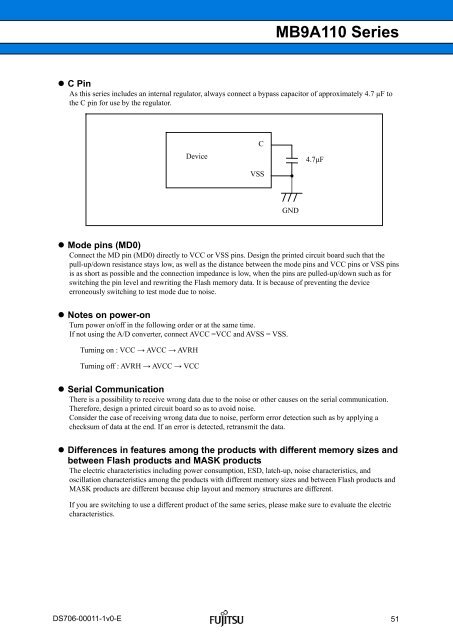
C Pin<br />
As this series includes an internal regulator, always connect a bypass capacitor of approximately 4.7 µF to<br />
the C pin for use by the regulator.<br />
DS706-00011-1v0-E<br />
Device<br />
Mode pins (MD0)<br />
Connect the MD pin (MD0) directly to VCC or VSS pins. Design the printed circuit board such that the<br />
pull-up/down resistance stays low, as well as the distance between the mode pins and VCC pins or VSS pins<br />
is as short as possible and the connection impedance is low, when the pins are pulled-up/down such as for<br />
switching the pin level and rewriting the Flash memory data. It is because of preventing the device<br />
erroneously switching to test mode due to noise.<br />
Notes on power-on<br />
Turn power on/off in the following order or at the same time.<br />
If not using the A/D converter, connect AVCC =VCC and AVSS = VSS.<br />
Turning on : VCC → AVCC → AVRH<br />
Turning off : AVRH → AVCC → VCC<br />
Serial Communication<br />
There is a possibility to receive wrong data due to the noise or other causes on the serial communication.<br />
Therefore, design a printed circuit board so as to avoid noise.<br />
Consider the case of receiving wrong data due to noise, perform error detection such as by applying a<br />
checksum of data at the end. If an error is detected, retransmit the data.<br />
Differences in features among the products with different memory sizes and<br />
between Flash products and MASK products<br />
The electric characteristics including power consumption, ESD, latch-up, noise characteristics, and<br />
oscillation characteristics among the products with different memory sizes and between Flash products and<br />
MASK products are different because chip layout and memory structures are different.<br />
If you are switching to use a different product of the same series, please make sure to evaluate the electric<br />
characteristics.<br />
C<br />
VSS<br />
GND<br />
4.7μF<br />
51