ATtiny2313 Datasheet - DCE FEL ČVUT v Praze
ATtiny2313 Datasheet - DCE FEL ČVUT v Praze
ATtiny2313 Datasheet - DCE FEL ČVUT v Praze
Create successful ePaper yourself
Turn your PDF publications into a flip-book with our unique Google optimized e-Paper software.
Serial<br />
Programming Pin<br />
Mapping<br />
Parallel<br />
Programming<br />
Enter Programming<br />
Mode<br />
Considerations for<br />
Efficient Programming<br />
2543K–AVR–03/10<br />
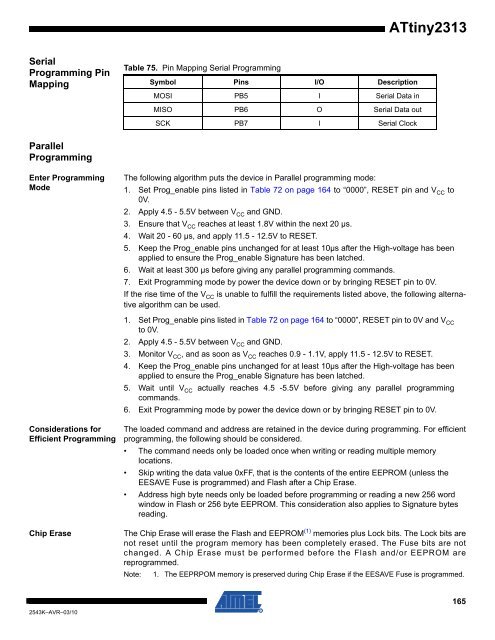
Table 75. Pin Mapping Serial Programming<br />
Symbol Pins I/O Description<br />
MOSI PB5 I Serial Data in<br />
MISO PB6 O Serial Data out<br />
SCK PB7 I Serial Clock<br />
<strong>ATtiny2313</strong><br />
The following algorithm puts the device in Parallel programming mode:<br />
1. Set Prog_enable pins listed in Table 72 on page 164 to “0000”, RESET pin and VCC to<br />
0V.<br />
2. Apply 4.5 - 5.5V between VCC and GND.<br />
3. Ensure that VCC reaches at least 1.8V within the next 20 µs.<br />
4. Wait 20 - 60 µs, and apply 11.5 - 12.5V to RESET.<br />
5. Keep the Prog_enable pins unchanged for at least 10µs after the High-voltage has been<br />
applied to ensure the Prog_enable Signature has been latched.<br />
6. Wait at least 300 µs before giving any parallel programming commands.<br />
7. Exit Programming mode by power the device down or by bringing RESET pin to 0V.<br />
If the rise time of the VCC is unable to fulfill the requirements listed above, the following alternative<br />
algorithm can be used.<br />
1. Set Prog_enable pins listed in Table 72 on page 164 to “0000”, RESET pin to 0V and VCC to 0V.<br />
2. Apply 4.5 - 5.5V between VCC and GND.<br />
3. Monitor VCC, and as soon as VCC reaches 0.9 - 1.1V, apply 11.5 - 12.5V to RESET.<br />
4. Keep the Prog_enable pins unchanged for at least 10µs after the High-voltage has been<br />
applied to ensure the Prog_enable Signature has been latched.<br />
5. Wait until VCC actually reaches 4.5 -5.5V before giving any parallel programming<br />
commands.<br />
6. Exit Programming mode by power the device down or by bringing RESET pin to 0V.<br />
The loaded command and address are retained in the device during programming. For efficient<br />
programming, the following should be considered.<br />
• The command needs only be loaded once when writing or reading multiple memory<br />
locations.<br />
• Skip writing the data value 0xFF, that is the contents of the entire EEPROM (unless the<br />
EESAVE Fuse is programmed) and Flash after a Chip Erase.<br />
• Address high byte needs only be loaded before programming or reading a new 256 word<br />
window in Flash or 256 byte EEPROM. This consideration also applies to Signature bytes<br />
reading.<br />
Chip Erase The Chip Erase will erase the Flash and EEPROM (1) memories plus Lock bits. The Lock bits are<br />
not reset until the program memory has been completely erased. The Fuse bits are not<br />
changed. A Chip Erase must be performed before the Flash and/or EEPROM are<br />
reprogrammed.<br />
Note: 1. The EEPRPOM memory is preserved during Chip Erase if the EESAVE Fuse is programmed.<br />
165


