ATtiny2313 Datasheet - DCE FEL ČVUT v Praze
ATtiny2313 Datasheet - DCE FEL ČVUT v Praze
ATtiny2313 Datasheet - DCE FEL ČVUT v Praze

Create successful ePaper yourself
Turn your PDF publications into a flip-book with our unique Google optimized e-Paper software.
2543K–AVR–03/10<br />
<strong>ATtiny2313</strong><br />
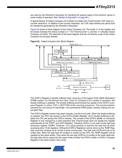
are used by the Waveform Generator for handling the special cases of the extreme values in<br />
some modes of operation (See “Modes of Operation” on page 96.)<br />
A special feature of Output Compare unit A allows it to define the Timer/Counter TOP value (i.e.,<br />
counter resolution). In addition to the counter resolution, the TOP value defines the period time<br />
for waveforms generated by the Waveform Generator.<br />
Figure 43 shows a block diagram of the Output Compare unit. The small “n” in the register and<br />
bit names indicates the device number (n = 1 for Timer/Counter 1), and the “x” indicates Output<br />
Compare unit (A/B). The elements of the block diagram that are not directly a part of the Output<br />
Compare unit are gray shaded.<br />
Figure 43. Output Compare Unit, Block Diagram<br />
TEMP (8-bit)<br />
OCRnxH Buf. (8-bit)<br />
OCRnx Buffer (16-bit Register)<br />
DATA BUS (8-bit)<br />
OCRnxL Buf. (8-bit)<br />
OCRnxH (8-bit) OCRnxL (8-bit)<br />
OCRnx (16-bit Register)<br />
TOP<br />
BOTTOM<br />
= (16-bit Comparator )<br />
Waveform Generator<br />
WGMn3:0<br />
COMnx1:0<br />
TCNTnH (8-bit) TCNTnL (8-bit)<br />
TCNTn (16-bit Counter)<br />
OCFnx (Int.Req.)<br />
The OCR1x Register is double buffered when using any of the twelve Pulse Width Modulation<br />
(PWM) modes. For the Normal and Clear Timer on Compare (CTC) modes of operation, the<br />
double buffering is disabled. The double buffering synchronizes the update of the OCR1x Compare<br />
Register to either TOP or BOTTOM of the counting sequence. The synchronization<br />
prevents the occurrence of odd-length, non-symmetrical PWM pulses, thereby making the output<br />
glitch-free.<br />
The OCR1x Register access may seem complex, but this is not case. When the double buffering<br />
is enabled, the CPU has access to the OCR1x Buffer Register, and if double buffering is disabled<br />
the CPU will access the OCR1x directly. The content of the OCR1x (Buffer or Compare)<br />
Register is only changed by a write operation (the Timer/Counter does not update this register<br />
automatically as the TCNT1 and ICR1 Register). Therefore OCR1x is not read via the high byte<br />
temporary register (TEMP). However, it is a good practice to read the low byte first as when<br />
accessing other 16-bit registers. Writing the OCR1x Registers must be done via the TEMP Register<br />
since the compare of all 16 bits is done continuously. The high byte (OCR1xH) has to be<br />
written first. When the high byte I/O location is written by the CPU, the TEMP Register will be<br />
updated by the value written. Then when the low byte (OCR1xL) is written to the lower eight bits,<br />
the high byte will be copied into the upper 8-bits of either the OCR1x buffer or OCR1x Compare<br />
Register in the same system clock cycle.<br />
OCnx<br />
93