GAL16V8 - svn
GAL16V8 - svn
GAL16V8 - svn

You also want an ePaper? Increase the reach of your titles
YUMPU automatically turns print PDFs into web optimized ePapers that Google loves.
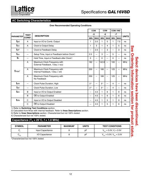
AC Switching Characteristics<br />
TEST<br />
PARAMETER<br />
COND1 .<br />
12<br />
Specifications <strong>GAL16V8</strong>D<br />
tpd A Input or I/O to Comb. Output 1 3.5 1 5 1 7.5 ns<br />
tco A Clock to Output Delay 1 3 1 4 1 5 ns<br />
tcf 2 — Clock to Feedback Delay — 2.5 — 3 — 3 ns<br />
tsu — Setup Time, Input or Feedback before Clock↑ 2.5 — 3 — 5 — ns<br />
th — Hold Time, Input or Feedback after Clock↑ 0 — 0 — 0 — ns<br />
fmax 3<br />
DESCRIPTION<br />
A Maximum Clock Frequency with 182 — 142.8 — 100 — MHz<br />
External Feedback, 1/(tsu + tco)<br />
A Maximum Clock Frequency with 200 — 166 — 125 — MHz<br />
Internal Feedback, 1/(tsu + tcf)<br />
A Maximum Clock Frequency with 250 — 166 — 125 — MHz<br />
No Feedback<br />
twh — Clock Pulse Duration, High 2 4 — 3 4 — 4 — ns<br />
twl — Clock Pulse Duration, Low 2 4 — 3 4 — 4 — ns<br />
ten B Input or I/O to Output Enabled — 4.5 1 6 1 9 ns<br />
B OE to Output Enabled — 4.5 1 6 1 6 ns<br />
tdis C Input or I/O to Output Disabled — 4.5 1 5 1 9 ns<br />
C OE to Output Disabled — 4.5 1 5 1 6 ns<br />
SYMBOL PARAMETER MAXIMUM* UNITS TEST CONDITIONS<br />
C I Input Capacitance 8 pF V CC = 5.0V, V I = 2.0V<br />
C I/O I/O Capacitance 8 pF V CC = 5.0V, V I/O = 2.0V<br />
*Characterized but not 100% tested.<br />
Over Recommended Operating Conditions<br />
1) Refer to Switching Test Conditions section.<br />
2) Calculated from fmax with internal feedback. Refer to fmax Descriptions section.<br />
3) Refer to fmax Descriptions section. Characterized but not 100% tested.<br />
4) Characterized but not 100% tested.<br />
Capacitance (T A = 25°C, f = 1.0 MHz)<br />
COM<br />
COM<br />
COM / IND<br />
-5 -7<br />
MIN. MAX. MIN. MAX. UNITS<br />
-3<br />
MIN. MAX.<br />
Select devices have been discontinued.<br />
See Ordering Information section for product status.