GAL16V8 - svn
GAL16V8 - svn
GAL16V8 - svn

Create successful ePaper yourself
Turn your PDF publications into a flip-book with our unique Google optimized e-Paper software.
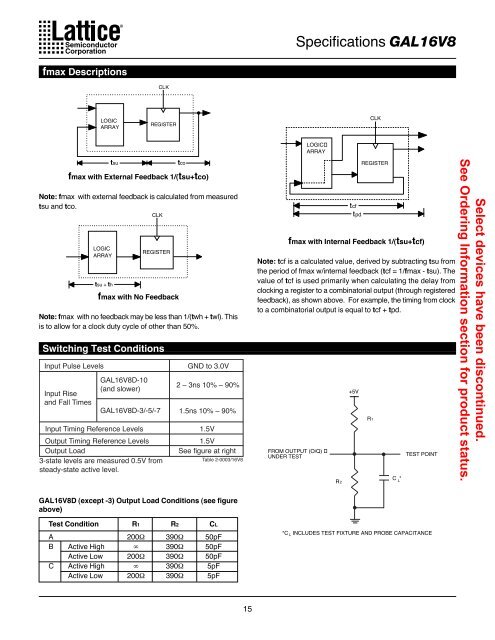
fmax Descriptions<br />
LOGIC<br />
ARRAY<br />
fmax with External Feedback 1/(tsu+tco)<br />
Note: fmax with external feedback is calculated from measured<br />
tsu and tco.<br />
LOGIC<br />
ARRAY<br />
tsu + th<br />
tsu<br />
REGISTER<br />
CLK<br />
CLK<br />
REGISTER<br />
fmax with No Feedback<br />
Note: fmax with no feedback may be less than 1/(twh + twl). This<br />
is to allow for a clock duty cycle of other than 50%.<br />
Switching Test Conditions<br />
Input Pulse Levels<br />
Input Rise<br />
and Fall Times<br />
<strong>GAL16V8</strong>D-10<br />
(and slower)<br />
<strong>GAL16V8</strong>D-3/-5/-7<br />
Input Timing Reference Levels<br />
Output Timing Reference Levels<br />
Output Load<br />
3-state levels are measured 0.5V from<br />
steady-state active level.<br />
Test Condition R1 R2 CL<br />
A 200Ω 390Ω 50pF<br />
B Active High ∞ 390Ω 50pF<br />
Active Low 200Ω 390Ω 50pF<br />
C Active High ∞ 390Ω 5pF<br />
Active Low 200Ω 390Ω 5pF<br />
tco<br />
GND to 3.0V<br />
2 – 3ns 10% – 90%<br />
1.5ns 10% – 90%<br />
1.5V<br />
1.5V<br />
See figure at right<br />
Table 2-0003/16V8<br />
<strong>GAL16V8</strong>D (except -3) Output Load Conditions (see figure<br />
above)<br />
15<br />
Specifications <strong>GAL16V8</strong><br />
LOGIC<br />
ARRAY<br />
tcf<br />
tpd<br />
CLK<br />
REGISTER<br />
fmax with Internal Feedback 1/(tsu+tcf)<br />
Note: tcf is a calculated value, derived by subtracting tsu from<br />
the period of fmax w/internal feedback (tcf = 1/fmax - tsu). The<br />
value of tcf is used primarily when calculating the delay from<br />
clocking a register to a combinatorial output (through registered<br />
feedback), as shown above. For example, the timing from clock<br />
to a combinatorial output is equal to tcf + tpd.<br />
FROM OUTPUT (O/Q)<br />
UNDER TEST<br />
R 2<br />
+5V<br />
C *<br />
L<br />
TEST POINT<br />
*C L INCLUDES TEST FIXTURE AND PROBE CAPACITANCE<br />
R 1<br />
Select devices have been discontinued.<br />
See Ordering Information section for product status.