

MPC5668x Data Sheet - Freescale Semiconductor
MPC5668x Data Sheet - Freescale Semiconductor
MPC5668x Data Sheet - Freescale Semiconductor

Create successful ePaper yourself
Turn your PDF publications into a flip-book with our unique Google optimized e-Paper software.
<strong>Freescale</strong> <strong>Semiconductor</strong><br />
<strong>Data</strong> <strong>Sheet</strong>: Technical <strong>Data</strong><br />
PXN20 Microcontroller <strong>Data</strong><br />
<strong>Sheet</strong><br />
PXN20 features:<br />
• 32-bit CPU core complex (e200z650)<br />
– Compliant with Power Architecture embedded category<br />
– 32 KB unified cache with line locking and eight-entry<br />
store buffer16<br />
– Execution speed static to 116 MHz<br />
• 32-bit I/O processor (e200z0)<br />
– Execution speed static to 1/2 CPU core speed (58 MHz)<br />
• 2 MB on-chip flash<br />
– Supports read during program and erase operations, and<br />
multiple blocks allowing EEPROM emulation<br />
• 512 KB + 80 KB (592 KB) on-chip ECC SRAM (PXN20)<br />
• 128 KB on-chip ECC SRAM (PXN21)<br />
• 16-entry Memory Protection Unit (PXN21 only)<br />
• Direct memory access controller<br />
– 16-channel on PXN20<br />
– 32-channel on PXN21<br />
• Fast ethernet controller<br />
– Supports 10-Mbps and 100-Mbps IEEE 802.3 MII,<br />
10-Mbps 7-wire interface<br />
– IEEE 802.3 MAC (compliant with IEEE 802.3 1998<br />
edition)<br />
• Media Local Bus (MLB) interface (PXN20 only)<br />
– Supports 16 logical channels, max speed 1024 Fs<br />
• Interrupt controller (INTC) supports 316 external interrupt<br />
vectors (22 are reserved)<br />
• System clocks<br />
– Frequency-modulated phase-locked loop (FMPLL)<br />
– 4–40MHz crystal oscillator (XTAL)<br />
– 32 kHz crystal oscillator (XTAL)<br />
– Dedicated 16 MHz and 128 kHz internal RC oscillators<br />
• Analog to Digital Converter (ADC) module<br />
– 10-bit A/D resolution<br />
– 32 external channels<br />
– 36 internal channels (PXN20)<br />
– 64 internal channels (PXN21)<br />
• Cross-Triggering Unit (PXN21 only)<br />
© <strong>Freescale</strong> <strong>Semiconductor</strong>, Inc., 2011. All rights reserved.<br />
Document Number: PXN20<br />
Rev. 1, 09/2011<br />
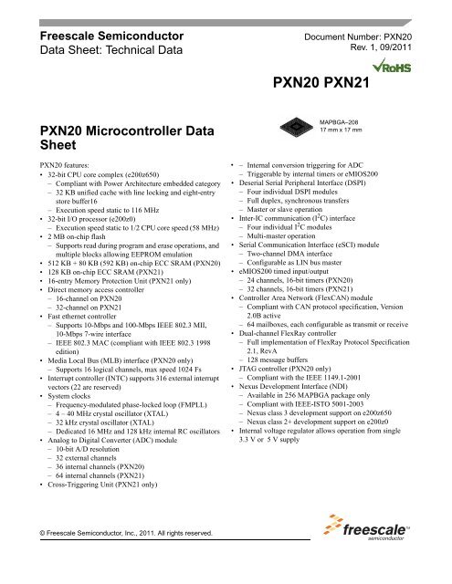
PXN20 PXN21<br />
MAPBGA–208<br />
17 mm x 17 mm<br />
• – Internal conversion triggering for ADC<br />
– Triggerable by internal timers or eMIOS200<br />
• Deserial Serial Peripheral Interface (DSPI)<br />
– Four individual DSPI modules<br />
– Full duplex, synchronous transfers<br />
– Master or slave operation<br />
• Inter-IC communication (I 2 C) interface<br />
– Four individual I 2 C modules<br />
– Multi-master operation<br />
• Serial Communication Interface (eSCI) module<br />
– Two-channel DMA interface<br />
– Configurable as LIN bus master<br />
• eMIOS200 timed input/output<br />
– 24 channels, 16-bit timers (PXN20)<br />
– 32 channels, 16-bit timers (PXN21)<br />
• Controller Area Network (FlexCAN) module<br />
– Compliant with CAN protocol specification, Version<br />
2.0B active<br />
– 64 mailboxes, each configurable as transmit or receive<br />
• Dual-channel FlexRay controller<br />
– Full implementation of FlexRay Protocol Specification<br />
2.1, RevA<br />
– 128 message buffers<br />
• JTAG controller (PXN20 only)<br />
– Compliant with the IEEE 1149.1-2001<br />
• Nexus Development Interface (NDI)<br />
– Available in 256 MAPBGA package only<br />
– Compliant with IEEE-ISTO 5001-2003<br />
– Nexus class 3 development support on e200z650<br />
– Nexus class 2+ development support on e200z0<br />
• Internal voltage regulator allows operation from single<br />
3.3 V or 5 V supply
1 Ordering information. . . . . . . . . . . . . . . . . . . . . . . . . . . . . . . . .3<br />
1.1 Orderable parts . . . . . . . . . . . . . . . . . . . . . . . . . . . . . . . .3<br />
1.2 PXN20 family feature set . . . . . . . . . . . . . . . . . . . . . . . .3<br />
2 PXN20 block diagrams . . . . . . . . . . . . . . . . . . . . . . . . . . . . . . .5<br />
3 Pin assignments . . . . . . . . . . . . . . . . . . . . . . . . . . . . . . . . . . . .7<br />
3.1 208-ball MAPBGA pin assignments . . . . . . . . . . . . . . . .7<br />
3.2 Pin muxing and reset states . . . . . . . . . . . . . . . . . . . . . .8<br />
4 Electrical characteristics . . . . . . . . . . . . . . . . . . . . . . . . . . . . .26<br />
4.1 Maximum ratings. . . . . . . . . . . . . . . . . . . . . . . . . . . . . .26<br />
4.2 Thermal characteristics. . . . . . . . . . . . . . . . . . . . . . . . .27<br />
4.3 ESD characteristics. . . . . . . . . . . . . . . . . . . . . . . . . . . .30<br />
4.4 VRC electrical specifications. . . . . . . . . . . . . . . . . . . . .30<br />
4.5 DC electrical specifications . . . . . . . . . . . . . . . . . . . . . .30<br />
2<br />
Table of Contents<br />
PXS30 Microcontroller <strong>Data</strong> <strong>Sheet</strong>, Rev. 1<br />
4.6 Operating current specifications . . . . . . . . . . . . . . 32<br />
4.7 I/O pad current specifications . . . . . . . . . . . . . . . . . . . 34<br />
4.8 Low voltage characteristics . . . . . . . . . . . . . . . . . . . . . 36<br />
4.9 Oscillators electrical characteristics. . . . . . . . . . . . . . . 36<br />
4.10 FMPLL electrical characteristics . . . . . . . . . . . . . . . . . 38<br />
4.11 ADC electrical characteristics . . . . . . . . . . . . . . . . . . . 39<br />
4.12 Flash memory electrical characteristics . . . . . . . . . . . 39<br />
4.13 Pad AC specifications . . . . . . . . . . . . . . . . . . . . . . . . . 40<br />
4.14 AC timing . . . . . . . . . . . . . . . . . . . . . . . . . . . . . . . . . . . 43<br />
5 Package characteristics. . . . . . . . . . . . . . . . . . . . . . . . . . . . . 58<br />
5.1 Package mechanical data . . . . . . . . . . . . . . . . . . . . . . 58<br />
6 Revision history. . . . . . . . . . . . . . . . . . . . . . . . . . . . . . . . . . . 60<br />
<strong>Freescale</strong> <strong>Semiconductor</strong>
1 Ordering information<br />
1.1 Orderable parts<br />
Table 1 shows the orderable part numbers for the PXN20 family.<br />
Qualification status<br />
Brand<br />
Family<br />
Class<br />
Flash memory size<br />
Temperature range<br />
Package identifier<br />
Operating frequency<br />
Tape and reel indicator<br />
Qualification status<br />
P = Pre-qualification (engineering samples)<br />
M = Fully spec. qualified, general market flow<br />
S = Fully spec. qualified, automotive flow<br />
Temperature range<br />
V = –40 °C to 105 °C<br />
(ambient)<br />
Package identifier<br />
MG = 208 MAPBGA<br />
1.2 PXN20 family feature set<br />
MPXN 20 20 V MG 116 R<br />
Family<br />
D = Display Graphics<br />
N = Connectivity/Network<br />
R = Performance/Real Time Control<br />
S=Safety<br />
Operating frequency<br />
116 = 116 MHz<br />
Note: Not all options are available on all devices. See Table 1 for more information.<br />
Figure 1. PXN20 orderable part number description<br />
Table 1. PXN20 orderable part number summary<br />
Part number Flash/SRAM Package<br />
PXN20 Microcontroller <strong>Data</strong> <strong>Sheet</strong>, Rev. 1<br />
Ordering information<br />
Speed<br />
(MHz)<br />
MPXN2020VMG116 2 MB / 592 KB 208 MAPBGA (17 mm x 17 mm) 116<br />
MPXN2120VMG116 2 MB / 128 KB 208 MAPBGA (17 mm x 17 mm) 116<br />
Table 2. PXN20 family feature set<br />
Flash Memory Size<br />
20 = 2 MB<br />
Tape and reel status<br />
R = Tape and reel<br />
(blank) = Trays<br />
Feature PXN20 PXN21<br />
Central Processing Unit (CPU) e200z650 e200z650<br />
Cache 32K, 4/8way 32K, 4/8way<br />
Floating Point Unit (FPU) Yes Yes<br />
Signal Processing Engine (SPE) Yes Yes<br />
Memory Management Unit (MMU) 32 entry 32 entry<br />
<strong>Freescale</strong> <strong>Semiconductor</strong> 3
Ordering information<br />
4<br />
Table 2. PXN20 family feature set (continued)<br />
Feature PXN20 PXN21<br />
CPU Execution Speed Static, 116 MHz Static, 116 MHz<br />
Input/Output Processor (IOP) e200z0 e200z0<br />
IOP Execution Speed 1/2 CPU execution speed 1/2 CPU execution speed<br />
Flash with ECC 2 MB 2 MB<br />
<strong>Data</strong> Flash Block 8x16 KB 8x16 KB<br />
RAM with ECC 592 KB 128 KB<br />
Memory Protection Unit (MPU) No 16 entry<br />
Direct Memory Access Unit (eDMA) 16 Channel 32 Channel<br />
Ethernet (FEC) Yes No<br />
MediaLB (MLB-DIM) Yes No<br />
FlexRay Controller Yes (128 Message Buffers) No<br />
Analog-to-Digital Converter (ADC) 36 internal channels, 10-bit<br />
Supports 32 external channels<br />
PXN20 Microcontroller <strong>Data</strong> <strong>Sheet</strong>, Rev. 1<br />
64 internal channels, 10-bit<br />
Supports 32 external channels<br />
Total Timer I/O (eMIOS200) 24 channels, 16-bit 32 channels, 16-bit<br />
Cross Trigger Unit (CTU) No Yes<br />
Asynchronous Serial Interfaces (UART) 6 12<br />
Synchronous Serial Interfaces (SPI) 4 4<br />
Controller Area Network (CAN) Controller 6 5<br />
Inter-Integrated Circuit (I 2 C) Controller 4 4<br />
Frequency Modulated PLL (FMPLL) Yes Yes<br />
4 – 40 MHz XTAL Oscillator Yes Yes<br />
16 MHz IRC Oscillator Yes Yes<br />
32 kHz XTAL Oscillator Yes Yes<br />
128 kHz IRC Oscillator Yes Yes<br />
Real Time Counter/ Autonomous Periodic Interrupts (RTC/API) Yes Yes<br />
Periodic Interrupt Timer (PIT) 8 8<br />
System Timer Module (STM) Yes Yes<br />
Software Watchdog Timer (SWT) Yes Yes<br />
General-Purpose I/O (GPIO) 155 155<br />
Clock Monitor (FMPLL) Yes Yes<br />
JTAG Yes Yes<br />
Nexus Debug (Only supported on emulation package) Nexus3 (e200Z6)<br />
Nexus2+ (e200Z0)<br />
Nexus3 (e200Z6)<br />
Nexus2+ (e200Z0)<br />
Production Package 208 MAPBGA 208 MAPBGA<br />
Emulation Package (for development use only) 256 MAPBGA 256 MAPBGA<br />
<strong>Freescale</strong> <strong>Semiconductor</strong>
2 PXN20 block diagrams<br />
Figure 2 shows a top-level block diagram of the PXN20 device.<br />
PXN20 Block Diagram<br />
Debug<br />
JTAG<br />
Nexus3 (Z6)<br />
Nexus2+ (Z0)<br />
e200z0 Core<br />
VLE<br />
2 MB<br />
Flash<br />
(ECC)<br />
ECSM<br />
Masters<br />
e200z650 Core<br />
VLE<br />
MMU (32 TLB)<br />
FPU/SPE<br />
32 KB Cache<br />
4/8 Way<br />
6 x UART/LIN<br />
36 x ADC<br />
24 x eMIOS<br />
PBRIDGE B<br />
16-ch DMA<br />
Mux<br />
32 kHz<br />
XTAL<br />
128 kHz<br />
IRC<br />
Crossbar Switch (XBAR)<br />
2 x I 2 C<br />
2 x SPI<br />
6 x CAN<br />
ADC – Analog-to-digital converter<br />
BAM – Boot assist module<br />
CAN – Controller area network controller<br />
ECC – Error correction code<br />
ECSM – Error correction status module<br />
eMIOS – Timed input/output<br />
eDMA – Enhanced direct memory access controller<br />
FEC – Fast ethernet controller<br />
FlexRay – FlexRay bus controller<br />
FMPLL – Frequency-modulated phase-locked loop<br />
I 2 C – Inter-integrated circuit controller<br />
INTC – Interrupt controller<br />
JTAG – Joint Test Action Group interface<br />
Figure 2. PXN20 block diagram<br />
4-40 MHz<br />
XTAL<br />
FMPLL<br />
Semaphores<br />
PXN20 Microcontroller <strong>Data</strong> <strong>Sheet</strong>, Rev. 1<br />
16 MHz<br />
IRC<br />
Ethernet MLB-DIM FlexRay<br />
PBRIDGE A<br />
2 x SPI<br />
2 x I 2 C<br />
80 KB<br />
SRAM<br />
(ECC)<br />
ECSM<br />
PXN20 block diagrams<br />
512 KB<br />
SRAM<br />
(ECC)<br />
Standby RAM<br />
ECSM<br />
VREG<br />
Controller<br />
RTC/API<br />
<strong>Freescale</strong> <strong>Semiconductor</strong> 5<br />
SWT<br />
STM<br />
INTC<br />
PIT<br />
BAM<br />
SIU<br />
MLB-DIM – Media Local Bus device interface module<br />
NDI – Nexus debug interface<br />
PBRIDGE– Peripheral I/O bridge<br />
PIT – Periodic interrupt timer<br />
RTC – Real time clock<br />
SIU – System integration unit<br />
SPI – Serial peripheral interface controller<br />
STM – System timer module<br />
SWT – Software watchdog timer<br />
UART/LIN – Universal asynchronous receiver/transmitter/<br />
local interconnect network<br />
VREG – Voltage regator
PXN20 block diagrams<br />
Figure 3 shows a top level block diagram for the PXN21 device.<br />
6<br />
PXN21 Block Diagram<br />
Debug<br />
JTAG<br />
Nexus3 (Z6)<br />
Nexus2+ (Z0)<br />
e200z0 Core<br />
VLE<br />
2 MB<br />
Flash<br />
(ECC)<br />
ECSM<br />
Masters<br />
e200z650 Core<br />
VLE<br />
MMU (32 TLB)<br />
FPU/SPE<br />
32 KB Cache<br />
4/8 Way<br />
32 kHz<br />
XTAL<br />
Crossbar Switch (XBAR)<br />
8 x UART/LIN<br />
64 x ADC<br />
32 x eMIOS<br />
PBRIDGE B<br />
CTU<br />
ADC – Analog-to-digital converter<br />
BAM – Boot assist module<br />
CAN – Controller area network controller<br />
CTU – Cross triggering unit<br />
ECC – Error correction code<br />
ECSM – Error correction status module<br />
eDMA – Enhanced direct memory access controller<br />
eMIOS – Timed input/output<br />
FMPLL – Frequency-modulated phase-locked loop<br />
I 2 C – Inter-integrated circuit controller<br />
INTC – Interrupt controller<br />
JTAG – Joint Test Action Group interface<br />
128 kHz<br />
IRC<br />
Semaphores<br />
32-ch DMA<br />
Mux<br />
4–40 MHz<br />
XTAL<br />
FMPLL<br />
Memory Protection Unit (MPU)<br />
2 x I 2 C<br />
2 x SPI<br />
5 x CAN<br />
Figure 3. PXN21 block diagram<br />
PBRIDGE A<br />
4 x UART/LIN<br />
2 x SPI<br />
2 x I 2 C<br />
PXN20 Microcontroller <strong>Data</strong> <strong>Sheet</strong>, Rev. 1<br />
16 MHz<br />
IRC<br />
VREG<br />
Controller<br />
RTC/API<br />
128 KB<br />
SRAM<br />
(ECC)<br />
SWT<br />
STM<br />
INTC<br />
PIT<br />
BAM<br />
SIU<br />
Standby RAM<br />
ECSM<br />
MPU – Memory protection unit<br />
NDI – Nexus debug interface<br />
PBRIDGE – Peripheral I/O bridge<br />
PIT – Periodic interrupt timer<br />
RTC – Real time clock<br />
SIU – System integration unit<br />
SPI – Serial peripheral interface controller<br />
STM – System timer module<br />
SWT – Software watchdog timer<br />
UART/LIN – Universal asynchronous receiver/transmitter/<br />
local interconnect network<br />
VREG – Voltage regulator<br />
<strong>Freescale</strong> <strong>Semiconductor</strong>
3 Pin assignments<br />
3.1 208-ball MAPBGA pin assignments<br />
Figure 4 shows the 208-ball MAPBGA pin assignments.<br />
A<br />
B<br />
C<br />
D<br />
E<br />
F<br />
1 2 3 4 5 6 7 8 9 10 11 12 13 14 15 16<br />
V SS<br />
PD2<br />
PD0<br />
PD1<br />
PD3 PD4<br />
PD7<br />
PD9<br />
PD6<br />
PD8<br />
PC12<br />
PC11<br />
PC14<br />
V DD<br />
V DD<br />
PC9<br />
PC7<br />
PC10 PC8 PC3 PB14 PB11 VRC VRCCTL PC13<br />
PC5<br />
V DDE1<br />
G PD11 PD12 PE4 VSS VSS VSS VSS VSS H<br />
J<br />
K<br />
L<br />
M<br />
N<br />
P<br />
R<br />
T<br />
PD5<br />
PD13<br />
PF1<br />
PF0<br />
PE6<br />
PD14<br />
PD15<br />
PE0<br />
PE1<br />
V SS<br />
PC1<br />
PC4<br />
Note: This ballmap is preliminary and<br />
should not be used for board<br />
design.<br />
Figure 4. PXN20 208-ball MAPBGA (full diagram)<br />
PXN20 Microcontroller <strong>Data</strong> <strong>Sheet</strong>, Rev. 1<br />
Pin assignments<br />
<strong>Freescale</strong> <strong>Semiconductor</strong> 7<br />
PC0<br />
V SS V SS V SS<br />
V SS V SS V SS<br />
V DD<br />
V SS<br />
V SS<br />
PB6<br />
PB7<br />
PB4<br />
PB5<br />
V DD33<br />
TEST<br />
PB0<br />
PB1<br />
PA8<br />
V DDA<br />
V SSA<br />
V SS<br />
V RH<br />
V RL<br />
PA10 PA12 PA0 PA14<br />
PA11 PA9 PA1 PA15<br />
PK1 PK2 JCOMP VDDEMLB VSS VSS VSS VSS VDD PG4 PG8 PG12<br />
PK0<br />
PF4<br />
PF10<br />
V SS<br />
PD10<br />
PF2 TDI<br />
PE7<br />
PG1<br />
PG0<br />
PE3<br />
PE5<br />
TMS<br />
TDO<br />
PE2<br />
PE8<br />
V DDE2<br />
PE9<br />
PC15<br />
PC2<br />
PC6<br />
PB13 PB10<br />
208 MAPBGA Ball Map<br />
(as viewed from top through the package)<br />
V DD<br />
EXTAL<br />
1 2 3 4 5 6 7 8 9 10 11 12 13 14 15 16<br />
PB15<br />
PB8<br />
PB12<br />
PF7 PF11 PK4 PK6 PK8 PJ0 PJ2 PJ4 PJ6<br />
PF9 PK3 PK5 PK7 PK9 PJ1 PJ3 PJ5 PJ7<br />
RESET<br />
PJ9<br />
PJ8<br />
V DDSYN<br />
PB9<br />
PJ13<br />
XTAL<br />
PB2<br />
PB3<br />
PA13<br />
V RCSEL<br />
V DDE3<br />
PG3<br />
PG5<br />
V SSSYN<br />
PA3<br />
PA7 PA5<br />
PF6 PF3 PE10 PE11 VDD PE15 PE14 PH9 PH11 VDDE4 PH15 PJ10 VSS PF12 PH3 PG15<br />
PF8 PF5 TCK PE12 PE13 PK10<br />
PH8 PH10 PH12 PH13 PH14 PJ11 PF15 PF14 PH4 PH1<br />
PG6<br />
PG7<br />
PJ12 PJ14 PH5 PH6<br />
PJ15<br />
PG2<br />
PF13<br />
PH0<br />
PG9<br />
PG10<br />
PH7<br />
PA2<br />
PA4<br />
PA6<br />
PG11<br />
PG13<br />
PG14<br />
PH2<br />
V SS<br />
A<br />
B<br />
C<br />
D<br />
E<br />
F<br />
G<br />
H<br />
J<br />
K<br />
L<br />
M<br />
N<br />
P<br />
R<br />
T
Pin assignments<br />
3.2 Pin muxing and reset states<br />
Table 3 shows the signals properties for each pin on PXN20. For all port pins that have an associated SIU_PCRn register to<br />
control pin properties, the supported functions column lists the functions associated with the programming of the<br />
SIU_PCRn[PA] bit in the order: general-purpose input/output (GPIO), function 1, function 2, and function 3 (see Figure 5).<br />
When an alternate function is not implemented for a value of SIU_PCRn[PA], a dash is shown in the Description column and<br />
the respective value in the PA bit field is reserved.<br />
Pin<br />
Name 1<br />
PA0 PA[0]<br />
AN[0]<br />
PA1 PA[1]<br />
AN[1]<br />
PA2 PA[2]<br />
AN[2]<br />
PA3 PA[3]<br />
AN[3]<br />
PA4 PA[4]<br />
AN[4]<br />
PA5 PA[5]<br />
AN[5]<br />
8<br />
Supported<br />
Functions 2<br />
Supported<br />
Functions 2<br />
PA[0]<br />
AN[0]<br />
GPIO<br />
(PCR)<br />
Num 3<br />
PA 4<br />
0 00<br />
01<br />
10<br />
11<br />
1 00<br />
01<br />
10<br />
11<br />
2 00<br />
01<br />
10<br />
11<br />
3 00<br />
01<br />
10<br />
11<br />
4 00<br />
01<br />
10<br />
11<br />
5 00<br />
01<br />
10<br />
11<br />
GPIO<br />
(PCR)<br />
Num 3<br />
0 00<br />
01<br />
10<br />
11<br />
Figure 5. Supported functions example<br />
Table 3. PXN20 signal properties<br />
Description<br />
Port A GPI<br />
ADC Analog Input<br />
—<br />
—<br />
Port A GPI<br />
ADC Analog Input<br />
—<br />
—<br />
Port A GPI<br />
ADC Analog Input<br />
—<br />
—<br />
Port A GPI<br />
ADC Analog Input<br />
—<br />
—<br />
Port A GPI<br />
ADC Analog Input<br />
—<br />
—<br />
Port A GPI<br />
ADC Analog Input<br />
—<br />
—<br />
PA 4 Description<br />
Port A GPI<br />
ADC Analog Input<br />
—<br />
—<br />
Port A (16)<br />
I/O<br />
Type<br />
I<br />
I<br />
—<br />
—<br />
I<br />
I<br />
—<br />
—<br />
I<br />
I<br />
—<br />
—<br />
I<br />
I<br />
—<br />
—<br />
I<br />
I<br />
—<br />
—<br />
I<br />
I<br />
—<br />
—<br />
Volt-<br />
age<br />
PXN20 Microcontroller <strong>Data</strong> <strong>Sheet</strong>, Rev. 1<br />
GPIO<br />
Function 1<br />
Functions 2 and 3<br />
not implemented<br />
Pad<br />
Type 5<br />
During<br />
Reset 6<br />
Status<br />
After<br />
Reset 7<br />
Package Pin<br />
Locations<br />
208<br />
BGA<br />
V DDA IHA — — D15<br />
V DDA IHA — — E15<br />
V DDA IHA — — F16<br />
V DDA IHA — — F15<br />
V DDA IHA — — G16<br />
V DDA IHA — — G15<br />
<strong>Freescale</strong> <strong>Semiconductor</strong>
Pin<br />
Name 1<br />
PA6 PA[6]<br />
AN[6]<br />
PA7 PA[7]<br />
AN[7]<br />
PA8 PA[8]<br />
AN[8]<br />
PA9 PA[9]<br />
AN[9]<br />
Supported<br />
Functions 2<br />
PA10 PA[10]<br />
AN[10]<br />
PA11 PA[11]<br />
AN[11]<br />
PA12 PA[12]<br />
AN[12]<br />
PA13 PA[13]<br />
AN[13]<br />
PA14 PA[14]<br />
AN[14]<br />
EXTAL32<br />
PA15 PA[15]<br />
AN[15]<br />
XTAL32<br />
GPIO<br />
(PCR)<br />
Num 3<br />
PA 4<br />
6 00<br />
01<br />
10<br />
11<br />
7 00<br />
01<br />
10<br />
11<br />
8 00<br />
01<br />
10<br />
11<br />
9 00<br />
01<br />
10<br />
11<br />
10 00<br />
01<br />
10<br />
11<br />
11 00<br />
01<br />
10<br />
11<br />
12 00<br />
01<br />
10<br />
11<br />
13 00<br />
01<br />
10<br />
11<br />
14 00<br />
01<br />
10<br />
11<br />
15 00<br />
01<br />
10<br />
11<br />
Table 3. PXN20 signal properties (continued)<br />
Description<br />
Port A GPI<br />
ADC Analog Input<br />
—<br />
—<br />
Port A GPI<br />
ADC Analog Input<br />
—<br />
—<br />
Port A GPI<br />
ADC Analog Input<br />
—<br />
—<br />
Port A GPI<br />
ADC Analog Input<br />
—<br />
—<br />
Port A GPI<br />
ADC Analog Input<br />
—<br />
—<br />
Port A GPI<br />
ADC Analog Input<br />
—<br />
—<br />
Port A GPI<br />
ADC Analog Input<br />
—<br />
—<br />
Port A GPI<br />
ADC Analog Input<br />
—<br />
—<br />
Port A GPI<br />
ADC Analog Input<br />
External 32 kHz Crystal In<br />
—<br />
Port A GPI<br />
ADC Analog Input<br />
External 32 kHz Crystal Out<br />
—<br />
PXN20 Microcontroller <strong>Data</strong> <strong>Sheet</strong>, Rev. 1<br />
Pin assignments<br />
<strong>Freescale</strong> <strong>Semiconductor</strong> 9<br />
I/O<br />
Type<br />
I<br />
I<br />
—<br />
—<br />
I<br />
I<br />
—<br />
—<br />
I<br />
I<br />
—<br />
—<br />
I<br />
I<br />
—<br />
—<br />
I<br />
I<br />
—<br />
—<br />
I<br />
I<br />
—<br />
—<br />
I<br />
I<br />
—<br />
—<br />
I<br />
I<br />
—<br />
—<br />
I<br />
I<br />
I<br />
—<br />
I<br />
I<br />
O<br />
—<br />
Volt-<br />
age<br />
Pad<br />
Type 5<br />
During<br />
Reset 6<br />
Status<br />
After<br />
Reset 7<br />
Package Pin<br />
Locations<br />
208<br />
BGA<br />
V DDA IHA — — H16<br />
V DDA IHA — — G14<br />
V DDA IHA — — F14<br />
V DDA IHA — — E14<br />
V DDA IHA — — D13<br />
V DDA IHA — — E13<br />
V DDA IHA — — D14<br />
V DDA IHA — — F13<br />
V DDA IHA — — D16<br />
V DDA IHA — — E16
Pin assignments<br />
Pin<br />
Name 1<br />
10<br />
Supported<br />
Functions 2<br />
PB0 PB[0]<br />
AN[16]/ANW<br />
PB1 PB[1]<br />
AN[17]/ANX<br />
PB2 PB[2]<br />
AN[18]/ANY<br />
PB3 PB[3]<br />
AN[19]/ANZ<br />
PB4 PB[4]<br />
AN[20]<br />
PB5 PB[5]<br />
AN[21]<br />
PB6 PB[6]<br />
AN[22]<br />
PB7 PB[7]<br />
AN[23]<br />
PB8 PB[8]<br />
AN[24]<br />
PCS_A[2]<br />
PB9 PB[9]<br />
AN[25]<br />
PCS_A[3]<br />
GPIO<br />
(PCR)<br />
Num 3<br />
PA 4<br />
16 00<br />
01<br />
10<br />
11<br />
17 00<br />
01<br />
10<br />
11<br />
18 00<br />
01<br />
10<br />
11<br />
19 00<br />
01<br />
10<br />
11<br />
20 00<br />
01<br />
10<br />
11<br />
21 00<br />
01<br />
10<br />
11<br />
22 00<br />
01<br />
10<br />
11<br />
23 00<br />
01<br />
10<br />
11<br />
24 00<br />
01<br />
10<br />
11<br />
25 00<br />
01<br />
10<br />
11<br />
Table 3. PXN20 signal properties (continued)<br />
Description<br />
Port B GPIO<br />
ADC Analog Input/Mux In<br />
—<br />
—<br />
Port B GPIO<br />
ADC Analog Input/Mux In<br />
—<br />
—<br />
Port B GPIO<br />
ADC Analog Input/Mux In<br />
—<br />
—<br />
Port B GPIO<br />
ADC Analog Input/Mux In<br />
—<br />
—<br />
Port B GPIO<br />
ADC Analog Input<br />
—<br />
—<br />
Port B GPIO<br />
ADC Analog Input<br />
—<br />
—<br />
Port B GPIO<br />
ADC Analog Input<br />
—<br />
—<br />
Port B GPIO<br />
ADC Analog Input<br />
—<br />
—<br />
Port B (16)<br />
Port B GPIO<br />
ADC Analog Input<br />
DSPI_A Peripheral Chip Select<br />
—<br />
Port B GPIO<br />
ADC Analog Input<br />
DSPI_A Peripheral Chip Select<br />
—<br />
I/O<br />
Type<br />
I/O<br />
I<br />
—<br />
—<br />
I/O<br />
I<br />
—<br />
—<br />
I/O<br />
I<br />
—<br />
—<br />
I/O<br />
I<br />
—<br />
—<br />
I/O<br />
I<br />
—<br />
—<br />
I/O<br />
I<br />
—<br />
—<br />
I/O<br />
I<br />
—<br />
—<br />
I/O<br />
I<br />
—<br />
—<br />
I/O<br />
I<br />
O<br />
—<br />
I/O<br />
I<br />
O<br />
—<br />
Volt-<br />
age<br />
PXN20 Microcontroller <strong>Data</strong> <strong>Sheet</strong>, Rev. 1<br />
Pad<br />
Type 5<br />
During<br />
Reset 6<br />
Status<br />
After<br />
Reset 7<br />
Package Pin<br />
Locations<br />
208<br />
BGA<br />
V DDE1 SHA — — B14<br />
V DDE1 SHA — — C14<br />
V DDE1 SHA — — B13<br />
V DDE1 SHA — — C13<br />
V DDE1 SHA — — C12<br />
V DDE1 SHA — — D12<br />
V DDE1 SHA — — C11<br />
V DDE1 SHA — — D11<br />
V DDE1 SHA — — A10<br />
V DDE1 SHA — — B12<br />
<strong>Freescale</strong> <strong>Semiconductor</strong>
Pin<br />
Name 1<br />
Supported<br />
Functions 2<br />
PB10 PB[10]<br />
AN[26]<br />
PCS_B[4]<br />
PB11 PB[11]<br />
AN[27]<br />
PCS_B[5]<br />
PB12 PB[12]<br />
AN[28]<br />
PCS_C[1]<br />
PB13 PB[13]<br />
AN[29]<br />
PCS_C[2]<br />
PB14 PB[14]<br />
AN[30]<br />
PCS_D[3]<br />
PB15 PB[15]<br />
AN[31]<br />
PCS_D[4]<br />
PC0 PC[0]<br />
AN[32]<br />
PC1 PC[1]<br />
AN[33]<br />
PC2 PC[2]<br />
AN[34]<br />
EVTI<br />
PC3 PC[3]<br />
AN[35]<br />
EVTO<br />
GPIO<br />
(PCR)<br />
Num 3<br />
PA 4<br />
26 00<br />
01<br />
10<br />
11<br />
27 00<br />
01<br />
10<br />
11<br />
28 00<br />
01<br />
10<br />
11<br />
29 00<br />
01<br />
10<br />
11<br />
30 00<br />
01<br />
10<br />
11<br />
31 00<br />
01<br />
10<br />
11<br />
32 00<br />
01<br />
10<br />
11<br />
33 00<br />
01<br />
10<br />
11<br />
34 00<br />
01<br />
10<br />
11<br />
35 00<br />
01<br />
10<br />
11<br />
Table 3. PXN20 signal properties (continued)<br />
Description<br />
Port B GPIO<br />
ADC Analog Input<br />
DSPI_B Peripheral Chip Select<br />
—<br />
Port B GPIO<br />
ADC Analog Input<br />
DSPI_B Peripheral Chip Select<br />
—<br />
Port B GPIO<br />
ADC Analog Input<br />
DSPI_C Peripheral Chip Select<br />
—<br />
Port B GPIO<br />
ADC Analog Input<br />
DSPI_C Peripheral Chip Select<br />
—<br />
Port B GPIO<br />
ADC Analog Input<br />
DSPI_D Peripheral Chip Select<br />
—<br />
Port B GPIO<br />
ADC Analog Input<br />
DSPI_D Peripheral Chip Select<br />
—<br />
Port C GPIO<br />
ADC Analog Input<br />
—<br />
—<br />
Port C GPIO<br />
ADC Analog Input<br />
—<br />
—<br />
Port C GPIO<br />
ADC Analog Input<br />
Nexus Event In<br />
—<br />
Port C GPIO<br />
ADC Analog Input<br />
Nexus Event Out<br />
—<br />
Port C (16)<br />
PXN20 Microcontroller <strong>Data</strong> <strong>Sheet</strong>, Rev. 1<br />
Pin assignments<br />
<strong>Freescale</strong> <strong>Semiconductor</strong> 11<br />
I/O<br />
Type<br />
I/O<br />
I<br />
O<br />
—<br />
I/O<br />
I<br />
O<br />
—<br />
I/O<br />
I<br />
O<br />
—<br />
I/O<br />
I<br />
O<br />
—<br />
I/O<br />
I<br />
O<br />
—<br />
I/O<br />
I<br />
O<br />
—<br />
I/O<br />
I<br />
—<br />
—<br />
I/O<br />
I<br />
—<br />
—<br />
I/O<br />
I<br />
I<br />
—<br />
I/O<br />
I<br />
O<br />
—<br />
Volt-<br />
age<br />
Pad<br />
Type 5<br />
During<br />
Reset 6<br />
Status<br />
After<br />
Reset 7<br />
Package Pin<br />
Locations<br />
208<br />
BGA<br />
V DDE1 SHA — — A9<br />
V DDE1 SHA — — B9<br />
V DDE1 SHA — — C10<br />
V DDE1 SHA — — A8<br />
V DDE1 SHA — — B8<br />
V DDE1 SHA — — C9<br />
V DDE1 SHA — — D9<br />
V DDE1 SHA — — C8<br />
V DDE1 SHA — — A7<br />
V DDE1 SHA — — B7
Pin assignments<br />
Pin<br />
Name 1<br />
12<br />
Supported<br />
Functions 2<br />
PC4 PC[4]<br />
AN[36]<br />
PC5 PC[5]<br />
AN[37]<br />
Z6NMI<br />
PC6 PC[6]<br />
AN[38]<br />
Z0NMI<br />
PC7 PC[7]<br />
AN[39]<br />
FR_DBG3<br />
PC8 PC[8]<br />
AN[40]<br />
FR_DBG2<br />
PC9 PC[9]<br />
AN[41]<br />
FR_DBG1<br />
PC10 PC[10]<br />
AN[42]<br />
FR_DBG0<br />
PC11 PC[11]<br />
AN[43]<br />
SCL_C<br />
PC12 PC[12]<br />
AN[44]<br />
SDA_C<br />
PC13 PC[13]<br />
AN[45]<br />
—<br />
MA[0]<br />
PC14 PC[14]<br />
AN[46]<br />
MA[1]<br />
GPIO<br />
(PCR)<br />
Num 3<br />
PA 4<br />
36 00<br />
01<br />
10<br />
11<br />
37 00<br />
01<br />
10<br />
11<br />
38 00<br />
01<br />
10<br />
11<br />
39 00<br />
01<br />
10<br />
11<br />
40 00<br />
01<br />
10<br />
11<br />
41 00<br />
01<br />
10<br />
11<br />
42 00<br />
01<br />
10<br />
11<br />
43 00<br />
01<br />
10<br />
11<br />
44 00<br />
01<br />
10<br />
11<br />
45 00<br />
01<br />
10<br />
11<br />
46 00<br />
01<br />
10<br />
11<br />
Table 3. PXN20 signal properties (continued)<br />
Description<br />
Port C GPIO<br />
ADC Analog Input<br />
—<br />
—<br />
Port C GPIO<br />
ADC Analog Input<br />
Z6 Core Non-Maskable Interrupt<br />
—<br />
Port C GPIO<br />
ADC Analog Input<br />
Z0 Core Non-Maskable Interrupt<br />
—<br />
Port C GPIO<br />
ADC Analog Input<br />
FlexRay Debug<br />
—<br />
Port C GPIO<br />
ADC Analog Input<br />
FlexRay Debug<br />
—<br />
Port C GPIO<br />
ADC Analog Input<br />
FlexRay Debug<br />
—<br />
Port C GPIO<br />
ADC Analog Input<br />
FlexRay Debug<br />
—<br />
Port C GPIO<br />
ADC Analog Input<br />
I 2 C_C Serial Clock<br />
—<br />
Port C GPIO<br />
ADC Analog Input<br />
I 2 C_C Serial <strong>Data</strong><br />
—<br />
Port C GPIO<br />
ADC Analog Input<br />
—<br />
ADC Ext. Mux Address Select<br />
Port C GPIO<br />
ADC Analog Input<br />
ADC Ext. Mux Address Select<br />
—<br />
I/O<br />
Type<br />
I/O<br />
I<br />
—<br />
—<br />
I/O<br />
I<br />
I<br />
—<br />
I/O<br />
I<br />
I<br />
—<br />
I/O<br />
I<br />
O<br />
—<br />
I/O<br />
I<br />
O<br />
—<br />
I/O<br />
I<br />
O<br />
—<br />
I/O<br />
I<br />
O<br />
—<br />
I/O<br />
I<br />
I/O<br />
—<br />
I/O<br />
I<br />
I/O<br />
—<br />
I/O<br />
I<br />
—<br />
O<br />
I/O<br />
I<br />
—<br />
O<br />
Volt-<br />
age<br />
PXN20 Microcontroller <strong>Data</strong> <strong>Sheet</strong>, Rev. 1<br />
Pad<br />
Type 5<br />
During<br />
Reset 6<br />
Status<br />
After<br />
Reset 7<br />
Package Pin<br />
Locations<br />
208<br />
BGA<br />
V DDE1 SHA — — D8<br />
V DDE1 SHA — — C6<br />
V DDE1 SHA — — C7<br />
V DDE1 SHA — — A6<br />
V DDE1 SHA — — B6<br />
V DDE1 SHA — — A5<br />
V DDE1 SHA — — B5<br />
V DDE1 SHA — — B4<br />
V DDE1 SHA — — A4<br />
V DDE1 SHA — — C5<br />
V DDE1 SHA — — C4<br />
<strong>Freescale</strong> <strong>Semiconductor</strong>
Pin<br />
Name 1<br />
Supported<br />
Functions 2<br />
PC15 PC[15]<br />
AN[47]<br />
MA[2]<br />
PD0 PD[0]<br />
CNTX_A<br />
PD1 PD[1]<br />
CNRX_A<br />
PD2 PD[2]<br />
CNTX_B<br />
PD3 PD[3]<br />
CNRX_B<br />
PD4 PD[4]<br />
CNTX_C<br />
PD5 PD[5]<br />
CNRX_C<br />
PD6 PD[6]<br />
CNTX_D<br />
TXD_K<br />
SCL_B<br />
PD7 PD[7]<br />
CNRX_D<br />
RXD_K<br />
SDA_B<br />
PD8 PD[8]<br />
CNTX_E<br />
TXD_L<br />
SCL_C<br />
GPIO<br />
(PCR)<br />
Num 3<br />
PA 4<br />
47 00<br />
01<br />
10<br />
11<br />
48 00<br />
01<br />
10<br />
11<br />
49 00<br />
01<br />
10<br />
11<br />
50 00<br />
01<br />
10<br />
11<br />
51 00<br />
01<br />
10<br />
11<br />
52 00<br />
01<br />
10<br />
11<br />
53 00<br />
01<br />
10<br />
11<br />
54 00<br />
01<br />
10<br />
11<br />
55 00<br />
01<br />
10<br />
11<br />
56 00<br />
01<br />
10<br />
11<br />
Table 3. PXN20 signal properties (continued)<br />
Description<br />
Port C GPIO<br />
ADC Analog Input<br />
ADC Ext. Mux Address Select<br />
—<br />
Port D GPIO<br />
FlexCAN_A Transmit<br />
—<br />
—<br />
Port D GPIO<br />
FlexCAN_A Receive<br />
—<br />
—<br />
Port D GPIO<br />
FlexCAN_B Transmit<br />
—<br />
—<br />
Port D GPIO<br />
FlexCAN_B Receive<br />
—<br />
—<br />
Port D GPIO<br />
FlexCAN_C Transmit<br />
—<br />
—<br />
Port D GPIO<br />
FlexCAN_C Receive<br />
—<br />
—<br />
Port D GPIO<br />
FlexCAN_D Transmit<br />
SCI_K Transmit<br />
I 2 C_B Serial Clock<br />
Port D GPIO<br />
FlexCAN_D Receive<br />
SCI_K Receive<br />
I 2 C_B Serial <strong>Data</strong><br />
Port D GPIO<br />
FlexCAN_E Transmit<br />
SCI_L Transmit<br />
I 2 C_C Serial Clock<br />
Port D (16)<br />
PXN20 Microcontroller <strong>Data</strong> <strong>Sheet</strong>, Rev. 1<br />
Pin assignments<br />
<strong>Freescale</strong> <strong>Semiconductor</strong> 13<br />
I/O<br />
Type<br />
I/O<br />
I<br />
O<br />
—<br />
I/O<br />
O<br />
—<br />
—<br />
I/O<br />
I<br />
—<br />
—<br />
I/O<br />
O<br />
—<br />
—<br />
I/O<br />
I<br />
—<br />
—<br />
I/O<br />
O<br />
—<br />
—<br />
I/O<br />
I<br />
—<br />
—<br />
I/O<br />
O<br />
O<br />
I/O<br />
I/O<br />
I<br />
I<br />
I/O<br />
I/O<br />
O<br />
O<br />
I/O<br />
Volt-<br />
age<br />
Pad<br />
Type 5<br />
During<br />
Reset 6<br />
Status<br />
After<br />
Reset 7<br />
Package Pin<br />
Locations<br />
208<br />
BGA<br />
V DDE1 SHA — — D5<br />
V DDE2 SH — — A2<br />
V DDE2 SH — — B2<br />
V DDE2 SH — — B1<br />
V DDE2 SH — — C1<br />
V DDE2 SH — — C2<br />
V DDE2 SH — — D1<br />
V DDE2 SH — — D2<br />
V DDE2 SH — — E1<br />
V DDE2 SH — — E2
Pin assignments<br />
Pin<br />
Name 1<br />
14<br />
Supported<br />
Functions 2<br />
PD9 PD[9]<br />
CNRX_E<br />
RXD_L<br />
SDA_C<br />
PD10 PD[10]<br />
CNTX_F<br />
TXD_M<br />
SCL_D<br />
PD11 PD[11]<br />
CNRX_F<br />
RXD_M<br />
SDA_D<br />
PD12 PD[12]<br />
TXD_A<br />
PD13 PD[13]<br />
RXD_A<br />
PD14 PD[14]<br />
TXD_B<br />
PD15 PD[15]<br />
RXD_B<br />
PE0 PE[0]<br />
TXD_C<br />
eMIOS[31]<br />
PE1 PE[1]<br />
RXD_C<br />
eMIOS[30]<br />
PE2 PE[2]<br />
TXD_D<br />
eMIOS[29]<br />
GPIO<br />
(PCR)<br />
Num 3<br />
PA 4<br />
57 00<br />
01<br />
10<br />
11<br />
58 00<br />
01<br />
10<br />
11<br />
59 00<br />
01<br />
10<br />
11<br />
60 00<br />
01<br />
10<br />
11<br />
61 00<br />
01<br />
10<br />
11<br />
62 00<br />
01<br />
10<br />
11<br />
63 00<br />
01<br />
10<br />
11<br />
64 00<br />
01<br />
10<br />
11<br />
65 00<br />
01<br />
10<br />
11<br />
66 00<br />
01<br />
10<br />
11<br />
Table 3. PXN20 signal properties (continued)<br />
Description<br />
Port D GPIO<br />
FlexCAN_E Receive<br />
SCI_L Receive<br />
I 2 C_C Serial <strong>Data</strong><br />
Port D GPIO<br />
FlexCAN_F Transmit<br />
SCI_M Transmit<br />
I 2 C_D Serial Clock<br />
Port D GPIO<br />
FlexCAN_F Receive<br />
SCI_M Receive<br />
I 2 C_D Serial <strong>Data</strong><br />
Port D GPIO<br />
eSCI_A Transmit<br />
—<br />
—<br />
Port D GPIO<br />
eSCI_A Receive<br />
—<br />
—<br />
Port D GPIO<br />
eSCI_B Transmit<br />
—<br />
—<br />
Port D GPIO<br />
eSCI_B Receive<br />
—<br />
—<br />
Port E GPIO<br />
eSCI_C Transmit<br />
eMIOS Channel<br />
—<br />
Port E GPIO<br />
eSCI_C Receive<br />
eMIOS Channel<br />
—<br />
Port E GPIO<br />
eSCI_D Transmit<br />
eMIOS Channel<br />
—<br />
Port E (16)<br />
I/O<br />
Type<br />
I/O<br />
I<br />
I<br />
I/O<br />
I/O<br />
O<br />
O<br />
I/O<br />
I/O<br />
I<br />
I<br />
I/O<br />
I/O<br />
O<br />
—<br />
—<br />
I/O<br />
I<br />
—<br />
—<br />
I/O<br />
O<br />
—<br />
—<br />
I/O<br />
I<br />
—<br />
—<br />
I/O<br />
O<br />
I/O<br />
—<br />
I/O<br />
I<br />
I/O<br />
I/O<br />
O<br />
I/O<br />
Volt-<br />
age<br />
PXN20 Microcontroller <strong>Data</strong> <strong>Sheet</strong>, Rev. 1<br />
Pad<br />
Type 5<br />
During<br />
Reset 6<br />
Status<br />
After<br />
Reset 7<br />
Package Pin<br />
Locations<br />
208<br />
BGA<br />
V DDE2 SH — — F1<br />
V DDE2 SH — — F2<br />
V DDE2 SH — — G1<br />
V DDE2 SH — — G2<br />
V DDE2 SH — — H1<br />
V DDE2 SH — — C3<br />
V DDE2 SH — — D3<br />
V DDE2 SH — — E3<br />
V DDE2 SH — — E4<br />
V DDE2 SH — — F4<br />
<strong>Freescale</strong> <strong>Semiconductor</strong>
Pin<br />
Name 1<br />
Supported<br />
Functions 2<br />
PE3 PE[3]<br />
RXD_D<br />
eMIOS[28]<br />
PE4 PE[4]<br />
TXD_E<br />
eMIOS[27]<br />
PE5 PE[5]<br />
RXD_E<br />
eMIOS[26]<br />
PE6 PE[6]<br />
TXD_F<br />
eMIOS[25]<br />
PE7 PE[7]<br />
RXD_F<br />
eMIOS[24]<br />
PE8 PE[8]<br />
TXD_G<br />
PCS_A[1]<br />
PE9 PE[9]<br />
RXD_G<br />
PCS_A[4]<br />
PE10 PE[10]<br />
TXD_H<br />
PCS_B[3]<br />
PE11 PE[11]<br />
RXD_H<br />
PCS_B[2]<br />
PE12 PE[12]<br />
TXD_J<br />
PCS_C[5]<br />
PE13 PE[13]<br />
RXD_J<br />
PCS_C[3]<br />
GPIO<br />
(PCR)<br />
Num 3<br />
PA 4<br />
67 00<br />
01<br />
10<br />
11<br />
68 00<br />
01<br />
10<br />
11<br />
69 00<br />
01<br />
10<br />
11<br />
70 00<br />
01<br />
10<br />
11<br />
71 00<br />
01<br />
10<br />
11<br />
72 00<br />
01<br />
10<br />
11<br />
73 00<br />
01<br />
10<br />
11<br />
74 00<br />
01<br />
10<br />
11<br />
75 00<br />
01<br />
10<br />
11<br />
76 00<br />
01<br />
10<br />
11<br />
77 00<br />
01<br />
10<br />
11<br />
Table 3. PXN20 signal properties (continued)<br />
Description<br />
Port E GPIO<br />
eSCI_D Receive<br />
eMIOS Channel<br />
—<br />
Port E GPIO<br />
eSCI_E Transmit<br />
eMIOS Channel<br />
—<br />
Port E GPIO<br />
eSCI_E Receive<br />
eMIOS Channel<br />
—<br />
Port E GPIO<br />
eSCI_F Transmit<br />
eMIOS Channel<br />
—<br />
Port E GPIO<br />
eSCI_F Receive<br />
eMIOS Channel<br />
—<br />
Port E GPIO<br />
eSCI_G Transmit<br />
DSPI_A Peripheral Chip Select<br />
—<br />
Port E GPIO<br />
eSCI_G Receive<br />
DSPI_A Peripheral Chip Select<br />
—<br />
Port E GPIO<br />
eSCI_H Transmit<br />
DSPI_B Peripheral Chip Select<br />
—<br />
Port E GPIO<br />
eSCI_H Receive<br />
DSPI_B Peripheral Chip Select<br />
—<br />
Port E GPIO<br />
eSCI_J Transmit<br />
DSPI_C Peripheral Chip Select<br />
—<br />
Port E GPIO<br />
eSCI_J Receive<br />
DSPI_C Peripheral Chip Select<br />
—<br />
PXN20 Microcontroller <strong>Data</strong> <strong>Sheet</strong>, Rev. 1<br />
Pin assignments<br />
<strong>Freescale</strong> <strong>Semiconductor</strong> 15<br />
I/O<br />
Type<br />
I/O<br />
I<br />
I/O<br />
I/O<br />
O<br />
I/O<br />
I/O<br />
I<br />
I/O<br />
I/O<br />
O<br />
I/O<br />
I/O<br />
I<br />
I/O<br />
I/O<br />
O<br />
O<br />
I/O<br />
I<br />
O<br />
I/O<br />
O<br />
O<br />
I/O<br />
I<br />
O<br />
I/O<br />
O<br />
O<br />
I/O<br />
I<br />
O<br />
Volt-<br />
age<br />
Pad<br />
Type 5<br />
During<br />
Reset 6<br />
Status<br />
After<br />
Reset 7<br />
Package Pin<br />
Locations<br />
208<br />
BGA<br />
V DDE2 SH — — F3<br />
V DDE2 SH — — G3<br />
V DDE2 SH — — H3<br />
V DDE2 SH — — M2<br />
V DDE2 SH — — L2<br />
V DDE2 SH — — J4<br />
V DDE2 SH — — M4<br />
V DDE2 SH — — N3<br />
V DDE2 SH — — N4<br />
V DDE2 SH — — P4<br />
V DDE2 SH — — P5
Pin assignments<br />
Pin<br />
Name 1<br />
16<br />
Supported<br />
Functions 2<br />
PE14 PE[14]<br />
SCL_A<br />
PCS_D[2]<br />
PE15 PE[15]<br />
SDA_A<br />
PCS_D[5]<br />
PF0 PF[0]<br />
SCK_A<br />
PF1 PF[1]<br />
SOUT_A<br />
PF2 PF[2]<br />
SIN_A<br />
PF3 PF[3]<br />
PCS_A[0]<br />
PCS_B[5]<br />
PCS_C[4]<br />
PF4 PF[4]<br />
SCK_B<br />
PCS_A[1]<br />
PCS_C[2]<br />
PF5 PF[5]<br />
SOUT_B<br />
PCS_A[2]<br />
PCS_C[3]<br />
PF6 PF[6]<br />
SIN_B<br />
PCS_A[3]<br />
PCS_C[5]<br />
PF7 PF[7]<br />
PCS_B[0]<br />
PCS_C[5]<br />
PCS_D[4]<br />
GPIO<br />
(PCR)<br />
Num 3<br />
PA 4<br />
78 00<br />
01<br />
10<br />
11<br />
79 00<br />
01<br />
10<br />
11<br />
80 00<br />
01<br />
10<br />
11<br />
81 00<br />
01<br />
10<br />
11<br />
82 00<br />
01<br />
10<br />
11<br />
83 00<br />
01<br />
10<br />
11<br />
84 00<br />
01<br />
10<br />
11<br />
85 00<br />
01<br />
10<br />
11<br />
86 00<br />
01<br />
10<br />
11<br />
87 00<br />
01<br />
10<br />
11<br />
Table 3. PXN20 signal properties (continued)<br />
Description<br />
Port E GPIO<br />
I 2 C_A Serial Clock<br />
DSPI_D Peripheral Chip Select<br />
—<br />
Port E GPIO<br />
I 2 C_A Serial <strong>Data</strong><br />
DSPI_D Peripheral Chip Select<br />
—<br />
Port F GPIO<br />
DSPI_A Serial Clock<br />
—<br />
—<br />
Port F GPIO<br />
DSPI_A Serial <strong>Data</strong> Out<br />
—<br />
—<br />
Port F GPIO<br />
DSPI_A Serial <strong>Data</strong> In<br />
—<br />
—<br />
Port F (16)<br />
Port F GPIO<br />
DSPI_A Peripheral Chip Select<br />
DSPI_B Peripheral Chip Select<br />
DSPI_C Peripheral Chip Select<br />
Port F GPIO<br />
DSPI_B Serial Clock<br />
DSPI_A Peripheral Chip Select<br />
DSPI_C Peripheral Chip Select<br />
Port F GPIO<br />
DSPI_B Serial <strong>Data</strong> Out<br />
DSPI_A Peripheral Chip Select<br />
DSPI_C Peripheral Chip Select<br />
Port F GPIO<br />
DSPI_B Serial <strong>Data</strong> In<br />
DSPI_A Peripheral Chip Select<br />
DSPI_C Peripheral Chip Select<br />
Port F GPIO<br />
DSPI_B Peripheral Chip Select<br />
DSPI_C Peripheral Chip Select<br />
DSPI_D Peripheral Chip Select<br />
I/O<br />
Type<br />
I/O<br />
I/O<br />
O<br />
—<br />
I/O<br />
I/O<br />
O<br />
—<br />
I/O<br />
I/O<br />
—<br />
—<br />
I/O<br />
O<br />
—<br />
—<br />
I/O<br />
I<br />
—<br />
—<br />
I/O<br />
I/O<br />
O<br />
O<br />
I/O<br />
I/O<br />
O<br />
O<br />
I/O<br />
O<br />
O<br />
O<br />
I/O<br />
I<br />
O<br />
O<br />
I/O<br />
I/O<br />
O<br />
O<br />
Volt-<br />
age<br />
PXN20 Microcontroller <strong>Data</strong> <strong>Sheet</strong>, Rev. 1<br />
Pad<br />
Type 5<br />
During<br />
Reset 6<br />
Status<br />
After<br />
Reset 7<br />
Package Pin<br />
Locations<br />
208<br />
BGA<br />
V DDE2 SH — — N7<br />
V DDE2 SH — — N6<br />
V DDE2 MH — — H2<br />
V DDE2 MH — — J1<br />
V DDE2 SH — — J2<br />
V DDE2 SH — — N2<br />
V DDE2 MH — — M1<br />
V DDE2 MH — — P2<br />
V DDE2 SH — — N1<br />
V DDE2 SH — — R2<br />
<strong>Freescale</strong> <strong>Semiconductor</strong>
Pin<br />
Name 1<br />
Supported<br />
Functions 2<br />
PF8 PF[8]<br />
SCK_C<br />
PF9 PF[9]<br />
SOUT_C<br />
PF10 PF[10]<br />
SIN_C<br />
PF11 PF[11]<br />
PCS_C[0]<br />
PCS_D[5]<br />
PCS_A[4]<br />
PF12 PF[12]<br />
SCK_D<br />
PF13 PF[13]<br />
SOUT_D<br />
PF14 PF[14]<br />
SIN_D<br />
PF15 PF[15]<br />
PCS_D[0]<br />
PCS_A[5]<br />
PCS_B[4]<br />
PG0 PG[0]<br />
PCS_A[4]<br />
PCS_B[3]<br />
AN[48]<br />
PG1 PG[1]<br />
PCS_A[5]<br />
PCS_B[4]<br />
AN[49]<br />
GPIO<br />
(PCR)<br />
Num 3<br />
PA 4<br />
88 00<br />
01<br />
10<br />
11<br />
89 00<br />
01<br />
10<br />
11<br />
90 00<br />
01<br />
10<br />
11<br />
91 00<br />
01<br />
10<br />
11<br />
92 00<br />
01<br />
10<br />
11<br />
93 00<br />
01<br />
10<br />
11<br />
94 00<br />
01<br />
10<br />
11<br />
95 00<br />
01<br />
10<br />
11<br />
96 00<br />
01<br />
10<br />
11<br />
97 00<br />
01<br />
10<br />
11<br />
Table 3. PXN20 signal properties (continued)<br />
Description<br />
Port F GPIO<br />
DSPI_C Serial Clock<br />
—<br />
—<br />
Port F GPIO<br />
DSPI_C Serial <strong>Data</strong> Out<br />
—<br />
—<br />
Port F GPIO<br />
DSPI_C Serial <strong>Data</strong> In<br />
—<br />
—<br />
Port F GPIO<br />
DSPI_C Peripheral Chip Select<br />
DSPI_D Peripheral Chip Select<br />
DSPI_A Peripheral Chip Select<br />
Port F GPIO<br />
DSPI_D Serial Clock<br />
—<br />
—<br />
Port F GPIO<br />
DSPI_D Serial <strong>Data</strong> Out<br />
—<br />
—<br />
Port F GPIO<br />
DSPI_D Serial <strong>Data</strong> In<br />
—<br />
—<br />
Port F GPIO<br />
DSPI_D Peripheral Chip Select<br />
DSPI_A Peripheral Chip Select<br />
DSPI_B Peripheral Chip Select<br />
Port G (16)<br />
Port G GPIO<br />
DSPI_A Peripheral Chip Select<br />
DSPI_B Peripheral Chip Select<br />
ADC Analog Input<br />
Port G GPIO<br />
DSPI_A Peripheral Chip Select<br />
DSPI_B Peripheral Chip Select<br />
ADC Analog Input<br />
PXN20 Microcontroller <strong>Data</strong> <strong>Sheet</strong>, Rev. 1<br />
Pin assignments<br />
<strong>Freescale</strong> <strong>Semiconductor</strong> 17<br />
I/O<br />
Type<br />
I/O<br />
I/O<br />
—<br />
—<br />
I/O<br />
O<br />
—<br />
—<br />
I/O<br />
I<br />
—<br />
—<br />
I/O<br />
I/O<br />
O<br />
O<br />
I/O<br />
I/O<br />
—<br />
—<br />
I/O<br />
O<br />
—<br />
—<br />
I/O<br />
I<br />
—<br />
—<br />
I/O<br />
I/O<br />
O<br />
O<br />
I/O<br />
O<br />
O<br />
I<br />
I/O<br />
O<br />
O<br />
I<br />
Volt-<br />
age<br />
Pad<br />
Type 5<br />
During<br />
Reset 6<br />
Status<br />
After<br />
Reset 7<br />
Package Pin<br />
Locations<br />
208<br />
BGA<br />
V DDE2 MH — — P1<br />
V DDE2 MH — — T2<br />
V DDE2 SH — — R1<br />
V DDE2 SH — — R3<br />
V DDE3 MH — — N14<br />
V DDE3 MH — — M14<br />
V DDE3 SH — — P14<br />
V DDE3 SH — — P13<br />
V DDE2 SHA — — B3<br />
V DDE2 SHA — — A3
Pin assignments<br />
Pin<br />
Name 1<br />
18<br />
Supported<br />
Functions 2<br />
PG2 PG[2]<br />
PCS_D[1]<br />
SCL_C<br />
AN[50]<br />
PG3 PG[3]<br />
PCS_D[2]<br />
SDA_C<br />
AN[51]<br />
PG4 PG[4]<br />
PCS_D[3]<br />
SCL_B<br />
AN[52]<br />
PG5 PG[5]<br />
PCS_D[4]<br />
SDA_B<br />
AN[53]<br />
PG6 PG[6]<br />
PCS_C[1]<br />
FEC_MDC<br />
AN[54]<br />
PG7 PG[7]<br />
PCS_C[2]<br />
FEC_MDIO<br />
AN[55]<br />
PG8 PG[8]<br />
eMIOS[7]<br />
FEC_TX_CLK<br />
AN[56]<br />
PG9 PG[9]<br />
eMIOS[6]<br />
FEC_CRS<br />
AN[57]<br />
PG10 PG[10]<br />
eMIOS[5]<br />
FEC_TX_ER<br />
AN[58]<br />
PG11 PG[11]<br />
eMIOS[4]<br />
FEC_RX_CLK<br />
AN[59]<br />
PG12 PG[12]<br />
eMIOS[3]<br />
FEC_TXD[0]<br />
AN[60]<br />
GPIO<br />
(PCR)<br />
Num 3<br />
PA 4<br />
98 00<br />
01<br />
10<br />
11<br />
99 00<br />
01<br />
10<br />
11<br />
100 00<br />
01<br />
10<br />
11<br />
101 00<br />
01<br />
10<br />
11<br />
102 00<br />
01<br />
10<br />
11<br />
103 00<br />
01<br />
10<br />
11<br />
104 00<br />
01<br />
10<br />
11<br />
105 00<br />
01<br />
10<br />
11<br />
106 00<br />
01<br />
10<br />
11<br />
107 00<br />
01<br />
10<br />
11<br />
108 00<br />
01<br />
10<br />
11<br />
Table 3. PXN20 signal properties (continued)<br />
Description<br />
Port G GPIO<br />
DSPI_D Peripheral Chip Select<br />
I 2 C_C Serial Clock<br />
ADC Analog Input<br />
Port G GPIO<br />
DSPI_D Peripheral Chip Select<br />
I 2 C_C Serial <strong>Data</strong><br />
ADC Analog Input<br />
Port G GPIO<br />
DSPI_D Peripheral Chip Select<br />
I 2 C_B Serial Clock<br />
ADC Analog Input<br />
Port G GPIO<br />
DSPI_D Peripheral Chip Select<br />
I 2 C_B Serial <strong>Data</strong><br />
ADC Analog Input<br />
Port G GPIO<br />
DSPI_C Peripheral Chip Select<br />
Ethernet Mgmt. <strong>Data</strong> Clock<br />
ADC Analog Input<br />
Port G GPIO<br />
DSPI_C Peripheral Chip Select<br />
Ethernet Mgmt. <strong>Data</strong> I/O<br />
ADC Analog Input<br />
Port G GPIO<br />
eMIOS Channel<br />
Ethernet Transmit Clock<br />
ADC Analog Input<br />
Port G GPIO<br />
eMIOS Channel<br />
Ethernet Carrier Sense<br />
ADC Analog Input<br />
Port G GPIO<br />
eMIOS Channel<br />
Ethernet Transmit Error<br />
ADC Analog Input<br />
Port G GPIO<br />
eMIOS Channel<br />
Ethernet Receive Clock<br />
ADC Analog Input<br />
Port G GPIO<br />
eMIOS Channel<br />
Ethernet Transmit <strong>Data</strong><br />
ADC Analog Input<br />
I/O<br />
Type<br />
I/O<br />
O<br />
I/O<br />
I<br />
I/O<br />
O<br />
I/O<br />
I<br />
I/O<br />
O<br />
I/O<br />
I<br />
I/O<br />
O<br />
I/O<br />
I<br />
I/O<br />
O<br />
O<br />
I<br />
I/O<br />
O<br />
I/O<br />
I<br />
I/O<br />
I/O<br />
I<br />
I<br />
I/O<br />
I/O<br />
I<br />
I<br />
I/O<br />
I/O<br />
O<br />
I<br />
I/O<br />
I/O<br />
I<br />
I<br />
I/O<br />
I/O<br />
O<br />
I<br />
Volt-<br />
age<br />
PXN20 Microcontroller <strong>Data</strong> <strong>Sheet</strong>, Rev. 1<br />
Pad<br />
Type 5<br />
During<br />
Reset 6<br />
Status<br />
After<br />
Reset 7<br />
Package Pin<br />
Locations<br />
208<br />
BGA<br />
V DDE3 SHA — — H14<br />
V DDE3 SHA — — J14<br />
V DDE3 SHA — — K14<br />
V DDE3 SHA — — L14<br />
V DDE3 MHA — — H15<br />
V DDE3 MHA — — J15<br />
V DDE3 SHA — — K15<br />
V DDE3 SHA — — L15<br />
V DDE3 MHA — — M15<br />
V DDE3 SHA — — J16<br />
V DDE3 MHA — — K16<br />
<strong>Freescale</strong> <strong>Semiconductor</strong>
Pin<br />
Name 1<br />
Supported<br />
Functions 2<br />
PG13 PG[13]<br />
eMIOS[2]<br />
FEC_TXD[1]<br />
AN[61]<br />
PG14 PG[14]<br />
eMIOS[1]<br />
FEC_TXD[2]<br />
AN[62]<br />
PG15 PG[15]<br />
eMIOS[0]<br />
FEC_TXD[3]<br />
AN[63]<br />
PH0 PH[0]<br />
eMIOS[31]<br />
FEC_COL<br />
PH1 PH[1]<br />
eMIOS[30]<br />
FEC_RX_DV<br />
PH2 PH[2]<br />
eMIOS[29]<br />
FEC_TX_EN<br />
PH3 PH[3]<br />
eMIOS[28]<br />
FEC_RX_ER<br />
PH4 PH[4]<br />
eMIOS[27]<br />
FEC_RXD[0]<br />
PH5 PH[5]<br />
eMIOS[26]<br />
FEC_RXD[1]<br />
PH6 PH[6]<br />
eMIOS[25]<br />
FEC_RXD[2]<br />
GPIO<br />
(PCR)<br />
Num 3<br />
PA 4<br />
109 00<br />
01<br />
10<br />
11<br />
110 00<br />
01<br />
10<br />
11<br />
111 00<br />
01<br />
10<br />
11<br />
112 00<br />
01<br />
10<br />
11<br />
113 00<br />
01<br />
10<br />
11<br />
114 00<br />
01<br />
10<br />
11<br />
115 00<br />
01<br />
10<br />
11<br />
116 00<br />
01<br />
10<br />
11<br />
117 00<br />
01<br />
10<br />
11<br />
118 00<br />
01<br />
10<br />
11<br />
Table 3. PXN20 signal properties (continued)<br />
Description<br />
Port G GPIO<br />
eMIOS Channel<br />
Ethernet Transmit <strong>Data</strong><br />
ADC Analog Input<br />
Port G GPIO<br />
eMIOS Channel<br />
Ethernet Transmit <strong>Data</strong><br />
ADC Analog Input<br />
Port G GPIO<br />
eMIOS Channel<br />
Ethernet Transmit <strong>Data</strong><br />
ADC Analog Input<br />
Port H GPIO<br />
eMIOS Channel<br />
Ethernet Collision<br />
—<br />
Port H (16)<br />
Port H GPIO<br />
eMIOS Channel<br />
Ethernet Receive <strong>Data</strong> Valid<br />
—<br />
Port H GPIO<br />
eMIOS Channel<br />
Ethernet Transmit Enable<br />
—<br />
Port H GPIO<br />
eMIOS Channel<br />
Ethernet Receive Error<br />
—<br />
Port H GPIO<br />
eMIOS Channel<br />
Ethernet Receive <strong>Data</strong><br />
—<br />
Port H GPIO<br />
eMIOS Channel<br />
Ethernet Receive <strong>Data</strong><br />
—<br />
Port H GPIO<br />
eMIOS Channel<br />
Ethernet Receive <strong>Data</strong><br />
—<br />
PXN20 Microcontroller <strong>Data</strong> <strong>Sheet</strong>, Rev. 1<br />
Pin assignments<br />
<strong>Freescale</strong> <strong>Semiconductor</strong> 19<br />
I/O<br />
Type<br />
I/O<br />
I/O<br />
O<br />
I<br />
I/O<br />
I/O<br />
O<br />
I<br />
I/O<br />
I/O<br />
O<br />
I<br />
I/O<br />
I/O<br />
I<br />
—<br />
I/O<br />
I/O<br />
I<br />
—<br />
I/O<br />
I/O<br />
O<br />
—<br />
I/O<br />
I/O<br />
I<br />
—<br />
I/O<br />
I/O<br />
I<br />
—<br />
I/O<br />
I/O<br />
I<br />
—<br />
I/O<br />
I/O<br />
I<br />
—<br />
Volt-<br />
age<br />
Pad<br />
Type 5<br />
During<br />
Reset 6<br />
Status<br />
After<br />
Reset 7<br />
Package Pin<br />
Locations<br />
208<br />
BGA<br />
V DDE3 MHA — — L16<br />
V DDE3 MHA — — M16<br />
V DDE3 MHA — — N16<br />
V DDE3 SH — — T14<br />
V DDE3 SH — — P16<br />
V DDE3 MH — — R16<br />
V DDE3 SH — — N15<br />
V DDE3 SH — — P15<br />
V DDE3 SH — — R14<br />
V DDE3 SH — — R15
Pin assignments<br />
Pin<br />
Name 1<br />
20<br />
Supported<br />
Functions 2<br />
PH7 PH[7]<br />
eMIOS[24]<br />
FEC_RXD[3]<br />
PH8 PH[8]<br />
eMIOS[23]<br />
PH9 PH[9]<br />
eMIOS[22]<br />
PH10 PH[10]<br />
eMIOS[21]<br />
PH11 PH[11]<br />
eMIOS[20]<br />
PH12 PH[12]<br />
eMIOS[19]<br />
PH13 PH[13]<br />
eMIOS[18]<br />
PH14 PH[14]<br />
eMIOS[17]<br />
PH15 PH[15]<br />
eMIOS[16]<br />
PJ0 PJ[0]<br />
eMIOS[15]<br />
PCS_A[4]<br />
GPIO<br />
(PCR)<br />
Num 3<br />
PA 4<br />
119 00<br />
01<br />
10<br />
11<br />
120 00<br />
01<br />
10<br />
11<br />
121 00<br />
01<br />
10<br />
11<br />
122 00<br />
01<br />
10<br />
11<br />
123 00<br />
01<br />
10<br />
11<br />
124 00<br />
01<br />
10<br />
11<br />
125 00<br />
01<br />
10<br />
11<br />
126 00<br />
01<br />
10<br />
11<br />
127 00<br />
01<br />
10<br />
11<br />
128 00<br />
01<br />
10<br />
11<br />
Table 3. PXN20 signal properties (continued)<br />
Description<br />
Port H GPIO<br />
eMIOS Channel<br />
Ethernet Receive <strong>Data</strong><br />
—<br />
Port H GPIO<br />
eMIOS Channel<br />
—<br />
—<br />
Port H GPIO<br />
eMIOS Channel<br />
—<br />
—<br />
Port H GPIO<br />
eMIOS Channel<br />
—<br />
—<br />
Port H GPIO<br />
eMIOS Channel<br />
—<br />
—<br />
Port H GPIO<br />
eMIOS Channel<br />
—<br />
—<br />
Port H GPIO<br />
eMIOS Channel<br />
—<br />
—<br />
Port H GPIO<br />
eMIOS Channel<br />
—<br />
—<br />
Port H GPIO<br />
eMIOS Channel<br />
—<br />
—<br />
Port J (16)<br />
Port J GPIO<br />
eMIOS Channel<br />
DSPI_A Peripheral Chip Select<br />
—<br />
I/O<br />
Type<br />
I/O<br />
I/O<br />
I<br />
—<br />
I/O<br />
I/O<br />
—<br />
—<br />
I/O<br />
I/O<br />
—<br />
—<br />
I/O<br />
I/O<br />
—<br />
—<br />
I/O<br />
I/O<br />
—<br />
—<br />
I/O<br />
I/O<br />
—<br />
—<br />
I/O<br />
I/O<br />
—<br />
—<br />
I/O<br />
I/O<br />
—<br />
—<br />
I/O<br />
I/O<br />
—<br />
—<br />
I/O<br />
I/O<br />
O<br />
—<br />
Volt-<br />
age<br />
PXN20 Microcontroller <strong>Data</strong> <strong>Sheet</strong>, Rev. 1<br />
Pad<br />
Type 5<br />
During<br />
Reset 6<br />
Status<br />
After<br />
Reset 7<br />
Package Pin<br />
Locations<br />
208<br />
BGA<br />
V DDE3 SH — — T15<br />
V DDE4 SH — — P7<br />
V DDE4 SH — — N8<br />
V DDE4 SH — — P8<br />
V DDE4 SH — — N9<br />
V DDE4 SH — — P9<br />
V DDE4 SH — — P10<br />
V DDE4 SH — — P11<br />
V DDE4 SH — — N11<br />
V DDE4 SH — — R7<br />
<strong>Freescale</strong> <strong>Semiconductor</strong>
Pin<br />
Name 1<br />
Supported<br />
Functions 2<br />
PJ1 PJ[1]<br />
eMIOS[14]<br />
PCS_A[5]<br />
PJ2 PJ[2]<br />
eMIOS[13]<br />
PCS_B[1]<br />
PJ3 PJ[3]<br />
eMIOS[12]<br />
PCS_B[2]<br />
PJ4 PJ[4]<br />
eMIOS[11]<br />
PCS_C[3]<br />
PJ5 PJ[5]<br />
eMIOS[10]<br />
PCS_C[4]<br />
PJ6 PJ[6]<br />
eMIOS[09]<br />
PCS_D[5]<br />
PJ7 PJ[7]<br />
eMIOS[08]<br />
PCS_D[1]<br />
PJ8 PJ[8]<br />
eMIOS[07]<br />
PJ9 PJ[9]<br />
eMIOS[06]<br />
PJ10 PJ[10]<br />
eMIOS[05]<br />
PJ11 PJ[11]<br />
eMIOS[04]<br />
GPIO<br />
(PCR)<br />
Num 3<br />
PA 4<br />
129 00<br />
01<br />
10<br />
11<br />
130 00<br />
01<br />
10<br />
11<br />
131 00<br />
01<br />
10<br />
11<br />
132 00<br />
01<br />
10<br />
11<br />
133 00<br />
01<br />
10<br />
11<br />
134 00<br />
01<br />
10<br />
11<br />
135 00<br />
01<br />
10<br />
11<br />
136 00<br />
01<br />
10<br />
11<br />
137 00<br />
01<br />
10<br />
11<br />
138 00<br />
01<br />
10<br />
11<br />
139 00<br />
01<br />
10<br />
11<br />
Table 3. PXN20 signal properties (continued)<br />
Description<br />
Port J GPIO<br />
eMIOS Channel<br />
DSPI_A Peripheral Chip Select<br />
—<br />
Port J GPIO<br />
eMIOS Channel<br />
DSPI_B Peripheral Chip Select<br />
—<br />
Port J GPIO<br />
eMIOS Channel<br />
DSPI_B Peripheral Chip Select<br />
—<br />
Port J GPIO<br />
eMIOS Channel<br />
DSPI_C Peripheral Chip Select<br />
—<br />
Port J GPIO<br />
eMIOS Channel<br />
DSPI_C Peripheral Chip Select<br />
—<br />
Port J GPIO<br />
eMIOS Channel<br />
DSPI_D Peripheral Chip Select<br />
—<br />
Port J GPIO<br />
eMIOS Channel<br />
DSPI_D Peripheral Chip Select<br />
—<br />
Port J GPIO<br />
eMIOS Channel<br />
—<br />
—<br />
Port J GPIO<br />
eMIOS Channel<br />
—<br />
—<br />
Port J GPIO<br />
eMIOS Channel<br />
—<br />
—<br />
Port J GPIO<br />
eMIOS Channel<br />
—<br />
—<br />
PXN20 Microcontroller <strong>Data</strong> <strong>Sheet</strong>, Rev. 1<br />
Pin assignments<br />
<strong>Freescale</strong> <strong>Semiconductor</strong> 21<br />
I/O<br />
Type<br />
I/O<br />
I/O<br />
O<br />
—<br />
I/O<br />
I/O<br />
O<br />
—<br />
I/O<br />
I/O<br />
O<br />
—<br />
I/O<br />
I/O<br />
O<br />
—<br />
I/O<br />
I/O<br />
O<br />
—<br />
I/O<br />
I/O<br />
O<br />
—<br />
I/O<br />
I/O<br />
O<br />
—<br />
I/O<br />
I/O<br />
—<br />
—<br />
I/O<br />
I/O<br />
—<br />
—<br />
I/O<br />
I/O<br />
—<br />
—<br />
I/O<br />
I/O<br />
—<br />
—<br />
Volt-<br />
age<br />
Pad<br />
Type 5<br />
During<br />
Reset 6<br />
Status<br />
After<br />
Reset 7<br />
Package Pin<br />
Locations<br />
208<br />
BGA<br />
V DDE4 SH — — T7<br />
V DDE4 SH — — R8<br />
V DDE4 SH — — T8<br />
V DDE4 SH — — R9<br />
V DDE4 SH — — T9<br />
V DDE4 SH — — R10<br />
V DDE4 SH — — T10<br />
V DDE4 SH — — T11<br />
V DDE4 SH — — R11<br />
V DDE4 SH — — N12<br />
V DDE4 SH — — P12
Pin assignments<br />
Pin<br />
Name 1<br />
22<br />
Supported<br />
Functions 2<br />
PJ12 PJ[12]<br />
eMIOS[03]<br />
PJ13 PJ[13]<br />
eMIOS[02]<br />
PJ14 PJ[14]<br />
eMIOS[01]<br />
PJ15 PJ[15]<br />
eMIOS[00]<br />
PK0 PK[0]<br />
MLBCLK<br />
SCK_B<br />
CLKOUT<br />
PK1 PK[1]<br />
MLBSIG<br />
SOUT_B<br />
PCS_D[4]<br />
PK2 PK[2]<br />
MLBDAT<br />
SIN_B<br />
PCS_D[5]<br />
PK3 PK[3]<br />
FR_A_RX<br />
MA[0]<br />
PCS_C[1]<br />
PK4 PK[4]<br />
FR_A_TX<br />
MA[1]<br />
PCS_C[2]<br />
PK5 PK[5]<br />
FR_A_TX_EN<br />
MA[2]<br />
PCS_C[3]<br />
GPIO<br />
(PCR)<br />
Num 3<br />
PA 4<br />
140 00<br />
01<br />
10<br />
11<br />
141 00<br />
01<br />
10<br />
11<br />
142 00<br />
01<br />
10<br />
11<br />
143 00<br />
01<br />
10<br />
11<br />
144 00<br />
01<br />
10<br />
11<br />
145 00<br />
01<br />
10<br />
11<br />
146 00<br />
01<br />
10<br />
11<br />
147 00<br />
01<br />
10<br />
11<br />
148 00<br />
01<br />
10<br />
11<br />
149 00<br />
01<br />
10<br />
11<br />
Table 3. PXN20 signal properties (continued)<br />
Description<br />
Port J GPIO<br />
eMIOS Channel<br />
—<br />
—<br />
Port J GPIO<br />
eMIOS Channel<br />
—<br />
—<br />
Port J GPIO<br />
eMIOS Channel<br />
—<br />
—<br />
Port J GPIO<br />
eMIOS Channel<br />
—<br />
—<br />
Port K GPIO<br />
Media Local Bus Clock<br />
DSPI_B Serial Clock<br />
CLKOUT (Test Only)<br />
Port K (11)<br />
Port K GPIO<br />
Media Local Bus Signal<br />
DSPI_B Serial <strong>Data</strong> Out<br />
DSPI_D Peripheral Chip Select<br />
Port K GPIO<br />
Media Local Bus <strong>Data</strong><br />
DSPI_B Serial <strong>Data</strong> In<br />
DSPI_D Peripheral Chip Select<br />
Port K GPIO<br />
FlexRay A Receive <strong>Data</strong><br />
ADC Ext. Mux Address Select<br />
DSPI_C Peripheral Chip Select<br />
Port K GPIO<br />
FlexRay A Transmit <strong>Data</strong><br />
ADC Ext. Mux Address Select<br />
DSPI_C Peripheral Chip Select<br />
Port K GPIO<br />
FlexRay A Transmit Enable<br />
ADC Ext. Mux Address Select<br />
DSPI_C Peripheral Chip Select<br />
I/O<br />
Type<br />
I/O<br />
I/O<br />
—<br />
—<br />
I/O<br />
I/O<br />
—<br />
—<br />
I/O<br />
I/O<br />
—<br />
—<br />
I/O<br />
I/O<br />
—<br />
—<br />
I/O<br />
I<br />
I/O<br />
O<br />
I/O<br />
I/O<br />
O<br />
O<br />
I/O<br />
I/O<br />
I<br />
O<br />
I/O<br />
I<br />
O<br />
O<br />
I/O<br />
O<br />
O<br />
O<br />
I/O<br />
O<br />
O<br />
O<br />
Volt-<br />
age<br />
PXN20 Microcontroller <strong>Data</strong> <strong>Sheet</strong>, Rev. 1<br />
Pad<br />
Type 5<br />
During<br />
Reset 6<br />
Status<br />
After<br />
Reset 7<br />
Package Pin<br />
Locations<br />
208<br />
BGA<br />
V DDE4 SH — — R12<br />
V DDE4 SH — — T12<br />
V DDE4 SH — — R13<br />
V DDE4 SH — — T13<br />
V DDEMLB F — — L1<br />
V DDEMLB F — — K1<br />
V DDEMLB F — — K2<br />
V DDE2 SH — — T3<br />
V DDE2 MH — — R4<br />
V DDE2 MH — — T4<br />
<strong>Freescale</strong> <strong>Semiconductor</strong>
Pin<br />
Name 1<br />
Supported<br />
Functions 2<br />
PK6 PK[6]<br />
FR_B_RX<br />
PCS_B[1]<br />
PCS_C[4]<br />
PK7 PK[7]<br />
FR_B_TX<br />
PCS_B[2]<br />
PCS_C[5]<br />
PK8 PK[8]<br />
FR_B_TX_EN<br />
PCS_B[3]<br />
PCS_A[1]<br />
PK9 PK[9]<br />
CLKOUT<br />
PCS_D[1]<br />
PCS_A[2]<br />
BOOTCFG<br />
PK10 PK[10]<br />
PCS_B[5]<br />
PCS_D[2]<br />
PCS_A[3]<br />
EXTAL EXTAL<br />
EXTCLK<br />
GPIO<br />
(PCR)<br />
Num 3<br />
PA 4<br />
150 00<br />
01<br />
10<br />
11<br />
151 00<br />
01<br />
10<br />
11<br />
152 00<br />
01<br />
10<br />
11<br />
153 00<br />
01<br />
10<br />
11<br />
154 00<br />
01<br />
10<br />
11<br />
Table 3. PXN20 signal properties (continued)<br />
Description<br />
Port K GPIO<br />
FlexRay B Receive <strong>Data</strong><br />
DSPI_B Peripheral Chip Select<br />
DSPI_C Peripheral Chip Select<br />
Port K GPIO<br />
FlexRay B Transmit <strong>Data</strong><br />
DSPI_B Peripheral Chip Select<br />
DSPI_C Peripheral Chip Select<br />
Port K GPIO<br />
FlexRay B Transmit Enable<br />
DSPI_B Peripheral Chip Select<br />
DSPI_A Peripheral Chip Select<br />
Port K GPIO<br />
CLKOUT (User mode)<br />
DSPI_D Peripheral Chip Select<br />
DSPI_A Peripheral Chip Select<br />
Boot Configuration<br />
Port K GPIO<br />
DSPI_B Peripheral Chip Select<br />
DSPI_D Peripheral Chip Select<br />
DSPI_A Peripheral Chip Select<br />
PXN20 Microcontroller <strong>Data</strong> <strong>Sheet</strong>, Rev. 1<br />
Pin assignments<br />
<strong>Freescale</strong> <strong>Semiconductor</strong> 23<br />
I/O<br />
I<br />
O<br />
O<br />
I/O<br />
O<br />
O<br />
O<br />
I/O<br />
O<br />
O<br />
O<br />
I/O<br />
O<br />
O<br />
O<br />
I<br />
I/O<br />
O<br />
O<br />
O<br />
Miscellaneous Pins (9)<br />
— — Main Crystal Oscillator Input<br />
External Clock Input<br />
I<br />
I<br />
V DDE2 SH — — R5<br />
V DDE2 MH — — T5<br />
V DDE2 MH — — R6<br />
V DDE2 MH BOOT<br />
CFG<br />
(Pulldown)<br />
GPIO T6<br />
V DDE2 SH — — P6<br />
V DDSYN A EXTAL A14<br />
XTAL XTAL — — Main Crystal Oscillator Output O V DDSYN A XTAL A13<br />
TDI TDI — — JTAG Test <strong>Data</strong> Input I V DDE2 SH TDI (Pull Up) J3<br />
TDO TDO — — JTAG Test <strong>Data</strong> Output O V DDE2 MH TDO (Pull Up 8 ) M3<br />
TMS TMS — — JTAG Test Mode Select Input I V DDE2 MH TMS (Pull Up) L3<br />
TCK TCK — — JTAG Test Clock Input I V DDE2 SH TCK (Pull Down) P3<br />
JCOMP JCOMP — — JTAG Compliancy I V DDE2 SH JCOMP (Pull Down) K3<br />
TEST TEST — — Test Mode Select I V DDE3 IH TEST 9 M13<br />
RESET RESET — — External Reset I/O VDDE1 MH RESET (Pull Up) A11<br />
1 The primary signal name is used as the pin label on the BGA map for identification purposes.<br />
2<br />
Each line in the Signal Name column corresponds to a separate signal function on the pin. For all device I/O pins, the primary,<br />
alternate, or GPIO signal functions are designated in the PA field of the System Integration Unit (SIU) PCR registers except<br />
where explicitly noted.<br />
3 The GPIO number is the same as the corresponding pad configuration register (SIU_PCRn) number.<br />
4 The PA bitfield in the SIU_PCRn register selects the signal function for the pin. A dash in the Description field of this table<br />
indicates that this value for PC is reserved on this pin, and should not be used.<br />
I/O<br />
Type<br />
Volt-<br />
age<br />
Pad<br />
Type 5<br />
During<br />
Reset 6<br />
Status<br />
After<br />
Reset 7<br />
Package Pin<br />
Locations<br />
208<br />
BGA
Pin assignments<br />
5<br />
The pad type is indicated by one or more of the following abbreviations: A–analog, F—fast speed, H–high voltage, I—input-only,<br />
M–medium speed, S–slow speed. For example, pad type SH designates a slow high-voltage pad.<br />
6<br />
The Status During Reset pin is sampled after the internal POR is negated. Prior to exiting POR, the signal has a high<br />
impedance. The terminology used in this column is: O – output, I – input, Up – weak pull up enabled, Down – weak pulldown<br />
enabled, Low – output driven low, High – output driven high. A dash on the left side of the slash denotes that both the input and<br />
output buffers for the pin are off. A dash on the right side of the slash denotes that there is no weak pull up/down enabled on<br />
the pin. The signal name to the left or right of the slash indicates the pin is enabled.<br />
7<br />
The Function After Reset of a GPI function is general purpose input. A dash on the left side of the slash denotes that both the<br />
input and output buffers for the pin are off. A dash on the right side of the slash denotes that there is no weak pull up/down<br />
enabled on the pin.<br />
8<br />
Pullup is enabled only when JCOMP is negated.<br />
9<br />
Tie to VSS for normal operation.<br />
24<br />
PXN20 Microcontroller <strong>Data</strong> <strong>Sheet</strong>, Rev. 1<br />
<strong>Freescale</strong> <strong>Semiconductor</strong>
3.2.1 Power and ground supply summary<br />
Pin<br />
Name<br />
Table 4. PXN20 power/ground<br />
Function Description Voltage 1<br />
1<br />
Nominal voltages.<br />
2 Base current to external NPN power transistor. Voltage may vary.<br />
PXN20 Microcontroller <strong>Data</strong> <strong>Sheet</strong>, Rev. 1<br />
Pin assignments<br />
Package Pin Locations<br />
VDD Internal Logic Power 1.2 V D4, D10, H4, G13, K13, N5<br />
VDDE1 External I/O Power 3.3–5.0 V D6<br />
VDDE2 L4<br />
VDDE3 J13<br />
VDDE4 N10<br />
VDDA Analog Power 3.3–5.0 V B15<br />
VDD33 3.3 V I/O Power 3.3 V L13<br />
VDDEMLB Media Local Bus Power 2.5 or 3.3 V K4<br />
VRCSEL Voltage Regulator Select VSSA / VDDA H13<br />
VRC Voltage Regulator Control Voltage 3.3–5.0 V B10<br />
VRCCTL Voltage Regulator Control Output — 2<br />
B11<br />
VDDSYN Clock Synthesizer Power 3.3 V A12<br />
VRH Analog High Voltage Reference 3.3–5.0 V B16<br />
VRL Analog Low Voltage Reference 0 V C16<br />
VSS Ground 0 V A1, A16, D7, G4, G[7:10], H[7:10],<br />
J[7:10], K[7:10], N13, T1, T16<br />
VSSA Analog Ground 0 V C15<br />
VSSSYN Clock Synthesizer Ground 0 V A15<br />
<strong>Freescale</strong> <strong>Semiconductor</strong> 25<br />
208
Electrical characteristics<br />
4 Electrical characteristics<br />
This section contains detailed information on power considerations, DC/AC electrical characteristics, and AC timing<br />
specifications for the PXN20.<br />
4.1 Maximum ratings<br />
26<br />
Table 5. Absolute maximum ratings 1<br />
Spec Characteristic Symbol Min Max Unit<br />
1 1.2 V Core Supply Voltage2 VDD –0.3 1.32 3<br />
V<br />
2 3.3 V Clock Synthesizer Voltage2, 4<br />
VDDSYN –0.3 3.6 V<br />
3 3.3 V I/O Buffer Voltage<br />
2, 4<br />
VDD33 –0.3 3.6 V<br />
4 3.3–5.0 V Voltage Regulator Control Voltage<br />
2, 5, 6<br />
VRC –0.3 5.5 V<br />
5 3.3–5.0 V Analog Supply Voltage (reference to VSSA )<br />
2, 5<br />
VDDA –0.3 5.5 V<br />
6 3.3–5.0 V External I/O Supply Voltage<br />
2, 5, 7<br />
V 8<br />
DDE1<br />
8<br />
VDDE2 V 8<br />
DDE3<br />
V 8<br />
DDE4<br />
–0.3<br />
–0.3<br />
–0.3<br />
–0.3<br />
5.5<br />
5.5<br />
5.5<br />
5.5<br />
V<br />
7 2.5–3.3 V External I/O Supply Voltage (MLB) 2, 4 V 8<br />
DDEMLB –0.3 3.6 V<br />
9 DC Input Voltage9 VDDE1, VDDE2, VDDE3, VDDE4 VDDEMLB, VDDENEX VIN –1.010 –1.0 9<br />
VDDEx + 0.3 V11 VDDEx + 0.3 V 10<br />
V<br />
10 Analog Reference High Voltage V RH –0.3 Minimum of<br />
5.5<br />
or<br />
V DDA +0.3<br />
11 Analog Reference Low Voltage VRL –0.3 5.5 V<br />
12 VSS to VSSA Differential Voltage VSS –VSSA –100 100 mV<br />
13 VSS to VSSSYN Differential Voltage VSS –VSSSYN –100 100 mV<br />
14 Maximum DC Digital Input Current12 (per pin, applies to all<br />
digital F, MH, SH, and IH pins)<br />
IMAXD –2 2 mA<br />
15 Maximum DC Analog Input Current 13 (per pin, applies to all<br />
analog AE and A pins)<br />
IMAXA –3 3 mA<br />
16 Storage Temperature Range TSTG –55.0 150.0<br />
o<br />
C<br />
17 Maximum Solder Temperature 14 TSDR — 235.0 oC 18 Moisture Sensitivity Level<br />
1 Functional operating conditions are given in the DC electrical specifications. Absolute maximum ratings are stress ratings only,<br />
and functional operation at the maxima is not guaranteed. Stress beyond the listed maxima may affect device reliability or<br />
cause permanent damage to the device.<br />
2<br />
Voltage overshoots during a high-to-low or low-to-high transition must not exceed 10 seconds per instance.<br />
15 MSL — 3<br />
3 2.0 V for 10 hours cumulative time, 1.2 V +10% for time remaining.<br />
4 5.3 V for 10 hours cumulative time, 3.3 V +10% for time remaining.<br />
5<br />
6.4 V for 10 hours cumulative time, 5.0 V +10% for time remaining.<br />
6<br />
VRC cannot be 100mV higher than VDDA. VDDSYN and VDD33 cannot be 100 mV higher than VRC.<br />
7 All functional non-supply I/O pins are clamped to VSS and V DDEx.<br />
PXN20 Microcontroller <strong>Data</strong> <strong>Sheet</strong>, Rev. 1<br />
V<br />
<strong>Freescale</strong> <strong>Semiconductor</strong>
4.2 Thermal characteristics<br />
PXN20 Microcontroller <strong>Data</strong> <strong>Sheet</strong>, Rev. 1<br />
Electrical characteristics<br />
8<br />
VDDEx are separate power segments and may be powered independently with no differential voltage constraints between the<br />
power segments.<br />
9<br />
AC signal over and undershoot of the input voltages of up to ±2.0 V is permitted for a cumulative duration of 60 hours over the<br />
complete lifetime of the device (injection current does not need to be limited for this duration).<br />
10<br />
Internal structures will hold the input voltage above –1.0 V if the injection current limit of 2 mA is met.<br />
11 Internal structures hold the input voltage below this maximum voltage on all pads powered by VDDE supplies, if the maximum<br />
injection current specification is met (25 mA for all pins) and VDDE is within Operating Voltage specifications.<br />
12<br />
Total injection current for all pins (including both digital and analog) must not exceed 25 mA.<br />
13 Total injection current for all analog input pins must not exceed 15 mA.<br />
14 Solder profile per CDF-AEC-Q100.<br />
15 Moisture sensitivity per JEDEC test method A112.<br />
Table 6. Thermal characteristics<br />
Spec Characteristic Symbol Unit<br />
4.2.1 General notes for specifications at maximum junction temperature<br />
An estimation of the chip junction temperature, T J , can be obtained from the equation:<br />
T J =T A +(R JA P D) Eqn. 1<br />
<strong>Freescale</strong> <strong>Semiconductor</strong> 27<br />
Value<br />
208 MAPBGA 256 MAPBGA<br />
1<br />
1, 2<br />
Junction to Ambient<br />
Natural Convection<br />
(Single layer board)<br />
RJA °C/W 39 39<br />
2<br />
1, 3<br />
Junction to Ambient<br />
Natural Convection<br />
(Four layer board 2s2p)<br />
RJA °C/W 24 24<br />
3<br />
1, 3<br />
Junction to Ambient<br />
(@200 ft./min., Single layer board)<br />
RJMA °C/W 31 31<br />
4<br />
1, 3<br />
Junction to Ambient<br />
(@200 ft./min., Four layer board 2s2p)<br />
RJMA °C/W 20 20<br />
5 Junction to Board<br />
1 Junction temperature is a function of on-chip power dissipation, package thermal resistance, mounting site (board)<br />
temperature, ambient temperature, air flow, power dissipation of other components on the board, and board thermal<br />
resistance.<br />
2<br />
Per SEMI G38-87 and JEDEC JESD51-2 with the single layer board horizontal.<br />
3 Per JEDEC JESD51-6 with the board horizontal.<br />
4<br />
RJB °C/W 13 13<br />
6 Junction to Case<br />
4<br />
Thermal resistance between the die and the printed circuit board per JEDEC JESD51-8. Board temperature is measured on<br />
the top surface of the board near the package.<br />
5<br />
RJC °C/W 6 6<br />
7 Junction to Package Top<br />
5 Indicates the average thermal resistance between the die and the case top surface as measured by the cold plate method (MIL<br />
SPEC-883 Method 1012.1) with the cold plate temperature used for the case temperature.<br />
6<br />
Natural Convection<br />
JT °C/W 2 2<br />
6<br />
Thermal characterization parameter indicating the temperature difference between package top and the junction temperature<br />
per JEDEC JESD51-2.
Electrical characteristics<br />
where:<br />
TA = ambient temperature for the package ( oC) RJA = junction to ambient thermal resistance ( o C/W)<br />
PD = power dissipation in the package (W)<br />
The supplied thermal resistances are provided based on JEDEC JESD51 series of standards to provide consistent values for<br />
estimations and comparisons. The difference between the values determined on the single-layer (1s) board and on the four-layer<br />
board with two signal layers and a power and a ground plane (2s2p) clearly demonstrate that the effective thermal resistance of<br />
the component is not a constant. It depends on the construction of the application board (number of planes), the effective size<br />
of the board which cools the component, how well the component is thermally and electrically connected to the planes, and the<br />
power being dissipated by adjacent components.<br />
Connect all the ground and power balls to the respective planes with one via per ball. Using fewer vias to connect the package<br />
to the planes reduces the thermal performance. Thinner planes also reduce the thermal performance. When the clearance<br />
between through vias leave the planes virtually disconnected, the thermal performance is also greatly reduced.<br />
As a general rule, the value obtained on a single layer board is appropriate for the tightly packed printed circuit board. The value<br />
obtained on the board with the internal planes is usually appropriate if the application board has one oz. (35 micron nominal<br />
thickness) internal planes, the components are well separated, and the overall power dissipation on the board is less than 0.02<br />
W/cm 2 .<br />
The thermal performance of any component depends strongly on the power dissipation of surrounding components. In addition,<br />
the ambient temperature varies widely within the application. For many natural convection and especially closed box<br />
applications, the board temperature at the perimeter (edge) of the package is approximately the same as the local air temperature<br />
near the device. Specifying the local ambient conditions explicitly as the board temperature provides a more precise description<br />
of the local ambient conditions that determine the temperature of the device.<br />
At a known board temperature, the junction temperature is estimated using the following equation:<br />
28<br />
T J =T B +(R JB P D) Eqn. 2<br />
where:<br />
TJ = junction temperature ( o C)<br />
TB = board temperature at the package perimeter ( oC/W) RJB = junction to board thermal resistance ( o C/W) per JESD51-8<br />
PD = power dissipation in the package (W)<br />
When the heat loss from the package case to the air can be ignored, acceptable predictions of junction temperature can be made.<br />
The application board should be similar to the thermal test condition, with the component soldered to a board with internal<br />
planes.<br />
Historically, the thermal resistance has frequently been expressed as the sum of a junction to case thermal resistance and a case<br />
to ambient thermal resistance:<br />
where:<br />
RJA = junction to ambient thermal resistance ( o C/W)<br />
RJC = junction to case thermal resistance ( oC/W) RCA = case to ambient thermal resistance ( o C/W)<br />
R JA =R JC +R CA<br />
PXN20 Microcontroller <strong>Data</strong> <strong>Sheet</strong>, Rev. 1<br />
Eqn. 3<br />
R JC is device related and cannot be influenced by the user. The user controls the thermal environment to change the case to<br />
ambient thermal resistance, R CA . For instance, the user can change the air flow around the device, add a heat sink, change the<br />
<strong>Freescale</strong> <strong>Semiconductor</strong>
PXN20 Microcontroller <strong>Data</strong> <strong>Sheet</strong>, Rev. 1<br />
Electrical characteristics<br />
mounting arrangement on printed circuit board, or change the thermal dissipation on the printed circuit board surrounding the<br />
device. This description is most useful for packages with heat sinks where some 90% of the heat flow is through the case to the<br />
heat sink to ambient. For most packages, a better model is required.<br />
A more accurate two-resistor thermal model can be constructed from the junction to board thermal resistance and the junction<br />
to case thermal resistance. The junction to case covers the situation where a heat sink will be used or where a substantial amount<br />
of heat is dissipated from the top of the package. The junction to board thermal resistance describes the thermal performance<br />
when most of the heat is conducted to the printed circuit board. This model can be used for either hand estimations or for a<br />
computational fluid dynamics (CFD) thermal model.<br />
To determine the junction temperature of the device in the application after prototypes are available, the Thermal<br />
Characterization Parameter (JT) can be used to determine the junction temperature with a measurement of the temperature at<br />
the top center of the package case using the following equation:<br />
T J =T T +( JT P D) Eqn. 4<br />
where:<br />
TT = thermocouple temperature on top of the package ( o C)<br />
JT = thermal characterization parameter ( oC/W) PD = power dissipation in the package (W)<br />
The thermal characterization parameter is measured per JESD51-2 specification using a 40-gauge type T thermocouple epoxied<br />
to the top center of the package case. The thermocouple should be positioned so that the thermocouple junction rests on the<br />
package. A small amount of epoxy is placed over the thermocouple junction and over about 1 mm of wire extending from the<br />
junction. The thermocouple wire is placed flat against the package case to avoid measurement errors caused by cooling effects<br />
of the thermocouple wire.<br />
References:<br />
<strong>Semiconductor</strong> Equipment and Materials International<br />
3081 Zanker Road<br />
San Jose, CA 95134<br />
(408) 943-6900<br />
MIL-SPEC and EIA/JESD (JEDEC) specifications are available from Global Engineering Documents at 800-854-7179 or<br />
303-397-7956.<br />
JEDEC specifications are available on the WEB at http://www.jedec.org.<br />
1. C.E. Triplett and B. Joiner, “An Experimental Characterization of a 272 PBGA Within an Automotive Engine<br />
Controller Module,” Proceedings of SemiTherm, San Diego, 1998, pp. 47–54.<br />
2. G. Kromann, S. Shidore, and S. Addison, “Thermal Modeling of a PBGA for Air-Cooled Applications,” Electronic<br />
Packaging and Production, pp. 53–58, March 1998.<br />
3. B. Joiner and V. Adams, “Measurement and Simulation of Junction to Board Thermal Resistance and Its Application<br />
in Thermal Modeling,” Proceedings of SemiTherm, San Diego, 1999, pp. 212–220.<br />
<strong>Freescale</strong> <strong>Semiconductor</strong> 29
Electrical characteristics<br />
4.3 ESD characteristics<br />
4.4 VRC electrical specifications<br />
4.5 DC electrical specifications<br />
30<br />
Table 7. ESD ratings1, 2<br />
Characteristic Symbol Value Unit<br />
ESD for Human Body Model (HBM) 2000 V<br />
HBM Circuit Description R1 1500 Ohm<br />
C 100 pF<br />
ESD for Field Induced Charge Model (FDCM) 750 (corner pins)<br />
Number of Pulses per pin:<br />
250 (all other pins)<br />
V<br />
Positive Pulses (HBM)<br />
—<br />
1<br />
—<br />
Negative Pulses (HBM)<br />
—<br />
1<br />
—<br />
Interval of Pulses — 1 second<br />
1 All ESD testing is in conformity with CDF-AEC-Q100 Stress Test Qualification for Automotive Grade Integrated Circuits.<br />
2 A device will be defined as a failure if after exposure to ESD pulses the device no longer meets the device specification<br />
requirements. Complete DC parametric and functional testing shall be performed per applicable device specification at room<br />
temperature followed by hot temperature, unless specified otherwise in the device specification.<br />
Table 8. VRC electrical specifications<br />
Spec Characteristic Symbol Min Max Units<br />
1 Current which can be sourced by V RCCTL I_V RCCTL 6.25 µA 20 mA —<br />
2<br />
Minimum Required Gain from external circuit:<br />
I DD / I_V RCCTL (@V DD =1.32V) 1<br />
–40C<br />
25C<br />
150C<br />
1 Assumes “typical usage” currents which will vary with application.<br />
Table 9. DC electrical specifications<br />
PXN20 Microcontroller <strong>Data</strong> <strong>Sheet</strong>, Rev. 1<br />
BETA 50<br />
50<br />
50 500<br />
Spec Characteristic Symbol Min Max Unit<br />
1 Maximum Operating Temperature Range — Die Junction Temperature TJ –40.0 150.0<br />
o<br />
C<br />
2 3.3 V Clock Synthesizer Voltage 1<br />
VDDSYN 3.0 3.6 V<br />
3 3.3 V I/O Buffer Voltage 1<br />
VDD33 3.0 3.6 V<br />
4 3.3–5.0 V Voltage Regulator Reference Voltage1 VRCSEL =VSSA VRCSEL =VDDA VVRC 3.0<br />
4.5<br />
3.6<br />
5.5<br />
V<br />
5 3.3–5.0 V Analog Supply Voltage V DDA maximum of<br />
3.0 V or<br />
V VRC –0.1<br />
5.5 V<br />
<strong>Freescale</strong> <strong>Semiconductor</strong>
6 3.3–5.0 V External I/O Supply Voltage 2<br />
V DDE1<br />
V DDE2<br />
V DDE3<br />
V DDE4<br />
PXN20 Microcontroller <strong>Data</strong> <strong>Sheet</strong>, Rev. 1<br />
Electrical characteristics<br />
7 2.5 V – 3.3 V External I/O Supply Voltage (MLB) V DDEMLB 3 2.375 3.6 V<br />
9 Pad Input High Voltage<br />
Hysteresis enabled<br />
4, 5<br />
Hysteresis disabled (IHA/SH/SHA/MH/MHA)<br />
Hysteresis disabled (F)<br />
10 Pad Input Low Voltage<br />
Hysteresis enabled<br />
4, 5<br />
Hysteresis disabled (IHA/SH/SHA/MH/MHA)<br />
Hysteresis disabled (F)<br />
<strong>Freescale</strong> <strong>Semiconductor</strong> 31<br />
V IH<br />
V IL<br />
3.0<br />
3.0<br />
3.0<br />
3.0<br />
0.65 V DDE<br />
0.55 V DDE<br />
0.55 V DDE<br />
V SS –0.3<br />
5.5<br />
5.5<br />
5.5<br />
5.5<br />
V<br />
V DDE +0.3 V<br />
0.35 V DDE<br />
0.40 V DDE<br />
0.40 V DDE<br />
11 Pad Input Hysteresis V HYS 0.1 V DDE V<br />
12 Analog (IHA) Input Voltage V INDC V SSA –0.3 V DDA +0.3 V<br />
13 Pad Output High Voltage 6, 7, 8 VOH 0.8 VDDE — V<br />
14 Pad Output Low Voltage 8<br />
VOL — 0.2 VDDE V<br />
15 Input Capacitance (Digital Pins: Pad type F, MH, SH) 4 CIN — 7 pF<br />
16<br />
4, 5<br />
Input Capacitance (Analog Pins: Pad type IHA) CIN_A — 10 pF<br />
17 Input Capacitance (Shared digital/analog pins: MHA, SHA) 4<br />
CIN_M — 12 pF<br />
18<br />
4, 9<br />
I/O Weak Pull Up/Down Absolute Current<br />
Pad F: 2.375 V – 3.6 V<br />
IACT 25 180<br />
A<br />
Pad SH/MH/IHA: 3.0 V – 3.6 V<br />
10 95<br />
Pad SH/MH/IHA: 4.5 V – 5.5 V<br />
35 200<br />
19 I/O Input Leakage Current 10<br />
Table 9. DC electrical specifications<br />
Spec Characteristic Symbol Min Max Unit<br />
I INACT_D –2.5 2.5 A<br />
20 DC Injection Current (per pin) IIC –1.0 1.0 mA<br />
21 Analog Input Current, Channel Off 11 4, 5<br />
(Analog pins IHA) IINACT_A –150 150 nA<br />
22 Analog Reference High Voltage V RH V DDA –500 V DDA mV<br />
23 Analog Reference Low Voltage V RL V SSA V SSA +500 mV<br />
24 V SS to V SSA Differential Voltage V SS –V SSA –100 100 mV<br />
25 V SSSYN to V SS Differential Voltage V SSSYN –V SS –100 100 mV<br />
26 Slew rate on V DDA , V DDEx , V DDSYN , V DD33 , and V RC power supply<br />
pins<br />
V Ramp — 100 V/ms<br />
27 Capacitive Supply Load (V DD ) V Load 8 — µF<br />
28 Capacitive Supply Load (VDD33, VDDSYN) VLoad 1 — µF<br />
1 When VRCSEL = VSSA (low), VDDSYN and VDD33 are externally supplied. When VRCSEL = VDDA (high), VDDSYN and VDD33 are<br />
generated by internal voltage regulators. When VRCSEL = VSSA (low), VDDSYN and VDD33 cannot be 100 mV higher than VRC. V
Electrical characteristics<br />
2 VDDE1 – V DDE4 are separate power segments and may be powered independently with no differential voltage constraints<br />
between the power segments. V DDE1 – V DDE3 pad power segments contain ADC analog input channels and thus the input<br />
analog signal level may be clamped to the V DDE level, resulting in inaccurate ADC results if the V DDE voltage level is less than<br />
V DDA.<br />
3 When VRCSEL = V DDA (high), the internally generated V DD33 voltage may be used to power V DDEMLB as long as the PK[0:2]<br />
pads remain in the disabled default state with their output buffers, input buffers, and pull devices disabled.<br />
4 The pad type is indicated by one or more of the following abbreviations: A–analog, F—fast speed, H–high voltage, I—input-only,<br />
M–medium speed, S–slow speed. For example, pad type SH designates a slow high-voltage pad.<br />
5 The IHA pads are related to VDDA.<br />
6 Characterization Based Capability:<br />
IOH_F = {12, 20, 30, 40} mA and IOL_F = {24, 40, 50, 65} mA for {00, 01,10, 11} drive mode with V DDE = 3.0 V;<br />
IOH_F = {7, 13, 18, 25} mA and IOL_F = {18, 30, 35, 50} mA for {00, 01, 10, 11} drive mode with V DDE =2.25 V;<br />
IOH_F = {3, 7, 10, 15} mA and IOL_F = {12, 20, 27, 35} mA for {00, 01, 10, 11} drive mode with V DDE =1.62 V.<br />
7 Characterization Based Capability:<br />
IOH_S = {6, 11.6} mA and IOL_S = {9.2, 17.7} mA for {slow, medium} I/O with V DDEH = 4.5 V;<br />
IOH_S = {2.8, 5.4} mA and IOL_S = {4.2, 8.1} mA for {slow, medium} I/O with V DDEH = 3.0 V<br />
8 All VOL /V OH values 100% tested with ±2 mA load.<br />
9 Absolute value of current, measured at VIL and V IH.<br />
10 Weak pull up/down inactive. Measured at VDDE = 5.25 V. Applies to pad types: SH and MH. Leakage specification guaranteed<br />
only when power supplies are within specified operating conditions.<br />
11 Maximum leakage occurs at maximum operating temperature. Leakage current decreases by approximately one-half for each<br />
8 to 12 o C, in the ambient temperature range of 50 to 125 o C. Applies to pad types: pad_a and pad_ae.<br />
4.6 Operating current specifications<br />
32<br />
Table 10. Operating currents<br />
Spec Characteristic Symbol<br />
Equations I TOTAL =I DDE +I DDA +I RH +I DD33 +I DDSYN +I RC +I DD<br />
I DDE =I DDE1 +I DDE2 +I DDE3 +I DDE4 +I DDEMLB<br />
1 VDDE Current<br />
VDDE(1,2,3,4) @ 3.0V–5.5V<br />
VDDEMLB @ 2.375V–3.6V<br />
Static 2<br />
Dynamic 3<br />
2 VDDA Current<br />
VDDA @ 3.0V–5.5V<br />
Run mode<br />
Sleep mode<br />
– Optional 32 kHz osc enabled<br />
3 VRH Current<br />
VRH @ 3.0V–5.5V<br />
Run mode<br />
Sleep mode<br />
4 VDD33 Current<br />
VDD33 @ 3.0V–3.6V<br />
Run mode<br />
Sleep mode<br />
PXN20 Microcontroller <strong>Data</strong> <strong>Sheet</strong>, Rev. 1<br />
Typ 1<br />
25 C<br />
Ambient<br />
Max 1<br />
–40–150 C<br />
Junction<br />
Unit<br />
— — — —<br />
I DDE<br />
I DDA<br />
I RH<br />
I DD33<br />
0<br />
Note 3<br />
1<br />
20<br />
+5<br />
300<br />
1<br />
10<br />
10<br />
30<br />
25<br />
30<br />
50<br />
+15<br />
700<br />
30<br />
20<br />
20<br />
A<br />
mA<br />
mA<br />
A<br />
A<br />
A<br />
A<br />
mA<br />
A<br />
<strong>Freescale</strong> <strong>Semiconductor</strong>
5 VDDSYN Current<br />
VDD33 @ 3.0V–3.6V<br />
Run mode<br />
Sleep mode<br />
– Optional 4 4–40 MHz osc enabled w/ no clock<br />
– Optional 4 4–40 MHz osc enabled w/ clock<br />
6 VRC Current (excluding IDD, IDD33, IDDSYN) 5<br />
VRC @ 3.135 V – 5.5 V<br />
Run mode<br />
Sleep mode<br />
– Optional 4 16MIRC enabled<br />
7 VDD Current<br />
VDD @ 1.08 V – 1.32 V<br />
Run mode (Maximum @ 116 MHz) 6<br />
Sleep mode<br />
– Optional 4 128KIRC enabled<br />
– Optional 4 16MIRC enabled<br />
– Optional 4 32 kHz osc enabled<br />
– Optional 4 4–40 MHz osc enabled w/ no clock<br />
– Optional 4 4–40 MHz osc enabled w/ clock<br />
– Optional 4 32 KB RAM<br />
– Optional 4 64 KB RAM<br />
– Optional 4 128 KB RAM<br />
Table 10. Operating currents (continued)<br />
Spec Characteristic Symbol<br />
I DDSYN<br />
PXN20 Microcontroller <strong>Data</strong> <strong>Sheet</strong>, Rev. 1<br />
Electrical characteristics<br />
1 Typ – Nominal voltage levels and functional activity. Max – Maximum voltage levels and functional activity.<br />
2 Static state of pins is when input pins are disabled or not being toggled and driven to a valid input level, output pins are not<br />
toggling or driving against any current loads, and internal pull devices are disabled or not pulling against any current loads.<br />
3 Dynamic current from pins is application-specific and depends on active pull devices, switching outputs, output capacitive and<br />
current loads, and switching inputs. Refer to Table 11 for more information.<br />
4 Optional currents are values that should be added to their respective current specifications to obtain the actual value for that<br />
specification when the optional function is active. The plus sign (+) in the Typ and Max columns indicates these optional<br />
currents. For example, V DDSYN in Sleep mode draws 1 .A (typ). With the optional 4–40 MHz osc enabled w/ no clock, add<br />
150 .A for a total of 151 .A (typ).<br />
5 VRC Current excluding the current supply to V DD33, V DDSYN and V DD from V RC.<br />
6 Maximum supply current transition: 50mA per 20S observation window.<br />
<strong>Freescale</strong> <strong>Semiconductor</strong> 33<br />
I RC<br />
I DD<br />
Typ 1<br />
25 C<br />
Ambient<br />
5<br />
1<br />
+150<br />
+300<br />
1<br />
0<br />
+40<br />
200<br />
100<br />
+5<br />
+200<br />
+5<br />
+5<br />
+150<br />
+10<br />
+20<br />
+40<br />
Max 1<br />
–40–150 C<br />
Junction<br />
10<br />
20<br />
+350<br />
+400<br />
10<br />
10<br />
+60<br />
340<br />
900<br />
+10<br />
+220<br />
+20<br />
+20<br />
+200<br />
+150<br />
+300<br />
+600<br />
Unit<br />
mA<br />
A<br />
A<br />
A<br />
mA<br />
A<br />
A<br />
mA<br />
A<br />
A<br />
A<br />
A<br />
A<br />
A<br />
A<br />
A<br />
A
Electrical characteristics<br />
4.7 I/O pad current specifications<br />
The power consumption of an I/O segment depends on the usage of the pins on a particular segment. The power consumption<br />
is the sum of all output pin currents for a particular segment. The output pin current can be calculated from Table 11 based on<br />
the voltage, frequency, and load on the pin. Use linear scaling to calculate pin currents for voltage, frequency, and load<br />
parameters that fall outside the values given in Table 11.<br />
Table 11. I/O pad average IDDE specifications 1<br />
19 Input IDRV_I_HV 7 0.5 5.5 N/A N/A N/A<br />
1<br />
These are typical values that are estimated from simulation and not tested. Currents apply to output pins only.<br />
34<br />
Spec<br />
1<br />
Pad<br />
Type 2<br />
Symbol<br />
Period<br />
(ns)<br />
Load 3<br />
(pF)<br />
2 Slow = SH or SHA; Medium = MH or MHA; Fast = F; Input = IHA. See Table 3.<br />
3 All loads are lumped.<br />
V DDE<br />
(V)<br />
Drive/Slew<br />
Rate Select<br />
PXN20 Microcontroller <strong>Data</strong> <strong>Sheet</strong>, Rev. 1<br />
I DDE Avg<br />
(mA)<br />
37 50 5.5 11 14<br />
2 130 50 5.5 01 5.3<br />
3<br />
Slow IDRV_SSR_HV 650 50 5.5 00 1.1<br />
4 840 200 5.5 00 3<br />
6<br />
24 50 5.5 11 9<br />
7 62 50 5.5 01 2.5<br />
8<br />
Medium IDRV_MSR_HV 317 50 5.5 00 0.5<br />
9 425 200 5.5 00 1.5<br />
11<br />
I DDE RMS<br />
(mA)<br />
10 50 3.6 11 50.4 101.6<br />
12 10 30 3.6 10 14.2 57.3<br />
13 10 20 3.6 01 16.4 43.6<br />
14 10 10 3.6 00 9.8 15.9<br />
15<br />
Fast IDRV_FC 10 50 2.75 11 22.9 45.3<br />
16 10 30 2.75 10 6.7 25.3<br />
17 10 20 2.75 01 4.5 17.3<br />
18 10 10 2.75 00 3 9.6<br />
<strong>Freescale</strong> <strong>Semiconductor</strong>
4.7.1 I/O pad V DD33 current specifications<br />
PXN20 Microcontroller <strong>Data</strong> <strong>Sheet</strong>, Rev. 1<br />
Electrical characteristics<br />
The power consumption of the VDD33 supply is dependent on the usage of the pins on all I/O segments. The power consumption<br />
is the sum of all input and output pin VDD33 currents for all I/O segments. The output pin VDD33 current can be calculated from<br />
Table 12 based on the voltage, frequency, and load on all Pad F pins. The input pin VDD33 current can be calculated from<br />
Table 12 based on the voltage, frequency, and load on all Pad MH pins. Use linear scaling to calculate pin currents for voltage,<br />
frequency, and load parameters that fall outside the values given in Table 12.<br />
Table 12. I/O pad average IDD33 specifications 1<br />
Spec<br />
1<br />
Pad<br />
Type 2<br />
Symbol<br />
Period<br />
(ns)<br />
Load 3<br />
(pF)<br />
9 Input IDRV_I_HV 7 0.5 N/A<br />
1<br />
These are typical values that are estimated from simulation and not tested. Currents apply to output pins only.<br />
2 Slow = SH or SHA; Medium = MH or MHA; Fast = F; Input = IHA. See Table 3.<br />
3 All loads are lumped.<br />
Drive<br />
Select<br />
I DD33 Avg<br />
(µA)<br />
I DD33 RMS<br />
(µA)<br />
100 50 11 0.8 235.7<br />
2 200 50 01 0.04 87.4<br />
3<br />
Slow IDRV_SSR_HV 800 50 00 0.06 47.4<br />
4 800 200 00 0.009 47<br />
5<br />
40 50 11<br />
6 100 50 01 0.11 76.5<br />
7<br />
Medium IDRV_MSR_HV 500 50 00 0.02 56.2<br />
8 500 200 00 0.01 56.2<br />
Spec<br />
1<br />
Pad<br />
Type 2<br />
Symbol<br />
Period<br />
(ns)<br />
Table 13. I DD33 pad average DC current 1<br />
Load 3<br />
(pF)<br />
8 10 10 3.6 2.75 00 1.06 4.09<br />
1 These are typical values that are estimated from simulation and not tested. Currents apply to output pins only.<br />
2 Slow = SH or SHA; Medium = MH or MHA; Fast = F; Input = IHA. See Table 3.<br />
3 All loads are lumped.<br />
V DD33<br />
(V)<br />
<strong>Freescale</strong> <strong>Semiconductor</strong> 35<br />
V DDE<br />
(V)<br />
Drive<br />
Select<br />
I DD33 Avg<br />
(µA)<br />
I DD33 RMS<br />
(µA)<br />
10 50 3.6 3.6 11 3.32 11.77<br />
2 10 30 3.6 3.6 10 2.28 7.07<br />
3 10 20 3.6 3.6 01 1.73 5.75<br />
4 10 10 3.6 3.6 00 1.39 4.77<br />
5<br />
Fast IDRV_FC 10 50 3.6 2.75 11 2.3 7.81<br />
6 10 30 3.6 2.75 10 1.64 4.96<br />
7 10 20 3.6 2.75 01 1.37 4.31
Electrical characteristics<br />
4.8 Low voltage characteristics<br />
4.9 Oscillators electrical characteristics<br />
36<br />
Table 14. Low voltage monitors<br />
Spec Characteristic Symbol Min Typical Max Unit<br />
1 Power-on-Reset Assert Level 1<br />
2 Low Voltage Monitor 3.3 V<br />
1<br />
Monitors VDDA.<br />
2<br />
Assert Level<br />
De-assert Level<br />
3 Low Voltage Monitor Synthesizer<br />
2<br />
Monitors VDD33.<br />
3<br />
Assert Level<br />
De-assert Level<br />
4 Low Voltage Monitor 3.0 V Low Threshold<br />
3 Monitors VDDSYN.<br />
1<br />
VRCSEL = VSSA Assert Level<br />
De-assert Level<br />
VRCSEL =VDDA Assert Level<br />
De-assert Level<br />
1, 4<br />
5 Low Voltage Monitor 5.0 V<br />
Assert Level<br />
De-assert Level<br />
1, 5<br />
6 Low Voltage Monitor 5.0 V High Threshold<br />
Assert Level<br />
De-assert Level<br />
4<br />
Disabled when VRCSEL =VSSA .<br />
PXN20 Microcontroller <strong>Data</strong> <strong>Sheet</strong>, Rev. 1<br />
V POR 1.5 — 2.8 V<br />
V LVI33A<br />
V LVI33D<br />
V LVISYNA<br />
V LVISYND<br />
V LVI_VDDA_LOA<br />
V LVI_VDDA_LOD<br />
V LVI_VDDA_LOA<br />
V LVI_VDDA_LOD<br />
V LVI_VDDA_A<br />
V LVI_VDDA_D<br />
V LVI_VDDA_HA<br />
V LVI_VDDA_HD<br />
3.00<br />
3.04<br />
3.00<br />
3.04<br />
3.00<br />
3.04<br />
3.25<br />
3.35<br />
4.35<br />
4.45<br />
4.50<br />
4.50<br />
Table 15. 3.3 V high frequency external oscillator<br />
3.05<br />
3.12<br />
3.05<br />
3.12<br />
3.05<br />
3.12<br />
3.35<br />
3.45<br />
4.475<br />
4.575<br />
4.675<br />
4.675<br />
Spec Characteristic Symbol Min Max Unit<br />
1 Frequency Range fref 4 1<br />
40 MHz<br />
2 Duty Cycle of reference tDC 40 60 %<br />
3 EXTAL Input High Voltage<br />
External crystal mode2 External clock mode<br />
VIHEXT VXTAL +0.4<br />
0.65 VDDSYN VDDSYN +0.3<br />
VDDSYN +0.3<br />
V<br />
4 EXTAL Input Low Voltage<br />
External crystal mode 3<br />
External clock mode<br />
V ILEXT<br />
V DDSYN –0.3<br />
V DDSYN –0.3<br />
3.10<br />
3.19<br />
3.10<br />
3.19<br />
3.10<br />
3.19<br />
3.48<br />
3.55<br />
4.55<br />
4.65<br />
4.80<br />
4.80<br />
V XTAL –0.4<br />
0.35 V DDSYN<br />
5 XTAL Current4 IXTAL 1 3 mA<br />
6 Total On-chip stray capacitance on XTAL CS_XTAL — 3 pF<br />
7 Total On-chip stray capacitance on EXTAL CS_EXTAL — 3 pF<br />
V<br />
V<br />
V<br />
V<br />
V<br />
V<br />
<strong>Freescale</strong> <strong>Semiconductor</strong>
8 Crystal manufacturer’s recommended<br />
capacitive load<br />
9 Discrete load capacitance to be connected<br />
to EXTAL<br />
10 Discrete load capacitance to be connected<br />
to XTAL<br />
C L<br />
See crystal<br />
specification<br />
PXN20 Microcontroller <strong>Data</strong> <strong>Sheet</strong>, Rev. 1<br />
Electrical characteristics<br />
See crystal<br />
specification<br />
C L_EXTAL — 2C L –C S_EXTAL –<br />
C PCB_EXTAL 5<br />
C L_XTAL — 2C L –C S_XTAL –C<br />
PCB_XTAL 5<br />
11 Startup Time tstartup — 10 ms<br />
1<br />
When PLL frequency modulation is active, reference frequencies less than 8 MHz will distort the modulated waveform and the<br />
effects of this on emissions is not characterized.<br />
2<br />
This parameter is meant for those who do not use quartz crystals or resonators, but instead use CAN oscillators in crystal<br />
mode. In that case, Vextal –Vxtal 400 mV criteria has to be met for oscillator’s comparator to produce output clock.<br />
3<br />
This parameter is meant for those who do not use quartz crystals or resonators, but instead use CAN oscillators in crystal<br />
mode. In that case, Vxtal –Vextal 400 mV criteria has to be met for oscillator’s comparator to produce output clock.<br />
4<br />
Ixtal is the oscillator bias current out of the XTAL pin with both EXTAL and XTAL pins grounded.<br />
5 CPCB_EXTAL and C PCB_XTAL are the measured PCB stray capacitances on EXTAL and XTAL, respectively.<br />
Table 16. 5 V low frequency (32 kHz) external oscillator<br />
Spec Characteristic Symbol Min Max Unit<br />
1 Frequency Range fref32 32 40 kHz<br />
2 Duty Cycle of reference tdc32 40 60 %<br />
3 XTAL32 Current1 IXTAL32 — 3 A<br />
4 Crystal manufacturer’s recommended<br />
capacitive load<br />
CL32 See crystal<br />
specification<br />
See crystal<br />
specification<br />
pF<br />
5 Startup Time tStartup — 2 s<br />
1<br />
Ixtal32 is the oscillator bias current out of the XTAL32 pin with both EXTAL32 and XTAL32 pins grounded.<br />
Table 17. 5 V High Frequency (16 MHz) internal RC oscillator<br />
Spec Characteristic Symbol Range Min Typ Max Unit<br />
1 Frequency before trim1 fut 35% 10.4 16 21.6 MHz<br />
2 Frequency after loading factory trim<br />
1 Across process, voltage, and temperature.<br />
2<br />
ft 7% 14.9 16 17.1 MHz<br />
3 Application trim resolution3 ts — — — 05 %<br />
4 Application frequency trim step3 fs — — 300 — kHz<br />
5 Startup Time tStartup — — — 500 ns<br />
2 Across voltage and temperature.<br />
3 Fixed voltage and temperature.<br />
Table 15. 3.3 V high frequency external oscillator (continued)<br />
Spec Characteristic Symbol Min Max Unit<br />
<strong>Freescale</strong> <strong>Semiconductor</strong> 37<br />
pF<br />
pF<br />
pF
Electrical characteristics<br />
4.10 FMPLL electrical characteristics<br />
38<br />
Table 18. 5V low frequency (128 kHz) internal RC oscillator<br />
Spec Characteristic Symbol Range Min Typ Max Unit<br />
1 Frequency before trim 1<br />
Fut128 35% 83.2 128 172.8 kHz<br />
2 Frequency after loading factory trim<br />
1<br />
Across process, voltage, and temperature.<br />
2<br />
Ft128 7% 119.0 128 137.0 kHz<br />
3 Application trim resolution3 Ts128 — — — 2 %<br />
4 Application frequency trim step 3<br />
Fs128 — — 4 — kHz<br />
5 Startup Time St128 — — — 100 s<br />
2 Across voltage and temperature.<br />
3 Fixed voltage and temperature.<br />
1 VDDSYN = 3.0 V to 3.6 V, V SS =V SSSYN =0V, T A =T L to T H.<br />
Table 19. FMPLL electrical specifications 1<br />
Spec Characteristic Symbol Min Max Unit<br />
1 System Frequency 2<br />
PXN20 Microcontroller <strong>Data</strong> <strong>Sheet</strong>, Rev. 1<br />
f SYS — 116 MHz<br />
2 PLL Reference Frequency Range f REF 4 40 MHz<br />
3 PLL Frequency fPLL f<br />
MHz<br />
vcomin -----------------------------<br />
ERFD + 1<br />
4 Loss of Reference Frequency 3 f LOR 100 2000 kHz<br />
5 Self Clocked Mode Frequency f SCM 16 64 MHz<br />
6 PLL Lock Time 4 t LPLL — 400 s<br />
7 Duty Cycle of Reference t DC 40 60 %<br />
8 Frequency un-LOCK Range f UL –4.0 4.0 % f SYS<br />
9 Frequency LOCK Range f LCK –2.0 2.0 % f SYS<br />
10<br />
CLKOUT Period Jitter, 5 Measured at f SYS Max<br />
Cycle-to-cycle Jitter<br />
C Jitter –5 5<br />
11 CLKOUT Jitter at 50 µs period C Jitter –250 250 ns<br />
12 Peak-to-Peak Frequency Modulation Range Limit 6,7<br />
(fSYSMax must not be exceeded)<br />
13 FM Depth Tolerance 8<br />
%f SYS<br />
C mod 0 4 %f SYS<br />
C mod_err –0.50 0.50 %f SYS<br />
14 VCO Frequency 9 f VCO 192 600 MHz<br />
15 Modulation Rate Limits 10 f MOD 0.400 1 MHz<br />
<strong>Freescale</strong> <strong>Semiconductor</strong>
4.11 ADC electrical characteristics<br />
4.12 Flash memory electrical characteristics<br />
PXN20 Microcontroller <strong>Data</strong> <strong>Sheet</strong>, Rev. 1<br />
Electrical characteristics<br />
2 The maximum frequency value is with frequency modulation disabled. If frequency modulation is enabled, the maximum<br />
frequency value should be de-rated by the percentage of modulation enabled so that the maximum frequency is not exceeded.<br />
3 “Loss of Reference Frequency” is the reference frequency detected internally, which transitions the PLL into self clocked mode.<br />
4 This specification applies to the period required for the PLL to re-lock after changing the MFD frequency control bits in the<br />
synthesizer control register (SYNCR). From power up with crystal oscillator reference, lock time will be additive with crystal<br />
startup time.<br />
5 Values are with frequency modulation disabled. If frequency modulation is enabled, jitter is the sum of Cjitter +C mod.<br />
6<br />
Modulation depth selected must not result in fPLL value greater than the fPLL maximum specified value.<br />
7<br />
Maximum and minimum variations from programmed modulation depth are 2%, 3%, and 4% peak-to-peak. Use only these<br />
settings.<br />
8<br />
Depth tolerance is the programmed modulation depth ±0.25% of fSYS .<br />
9<br />
See the Block Guide for VCO frequency synthesis equations.<br />
10<br />
Modulation rates less than 400 kHz will result in exceedingly long FM calibration durations. Modulation rates greater than<br />
1 MHz will result in reduced calibration accuracy.<br />
Table 20. ADC conversion specifications (operating)<br />
Spec Characteristic Symbol Min Max Unit<br />
1 Analog High Reference Voltage VRH VDDA –0.5 VDDA V<br />
2 Analog Low Reference Voltage VRL 0 0.5 V<br />
3 Analog Input Voltage AVIN VRL VRH V<br />
4 Sampling Frequency FS — 1.53 MHz<br />
5 Maximum ADC Clock Frequency FMAX — 60 MHz<br />
6 Sampling Time<br />
VDDA =3.0V–3.6V<br />
VDDA >3.6V–5.5V<br />
tS 250<br />
125<br />
— ns<br />
7 Differential Non Linearity DNL –1.0 1.0 LSB<br />
8 Integral Non Linearity INL –1.5 1.5 LSB<br />
9 Offset Error OFS –1.0 1.0 LSB<br />
10 Gain Error GNE –2.0 2.0 LSB<br />
11 Total Unadjusted Error 1<br />
TUE –2.0 2.0 LSB<br />
1 TUE assumes no pin activity on pins adjacent to analog channel or output driver activity on corresponding VDDE segment.<br />
Table 21. Flash program and erase specifications 1<br />
Spec Characteristic Symbol Min Initial<br />
Max 2 Max3 Unit<br />
1 Double Word (64 bits) Program Time4 tdwprogram — — 500 s<br />
2 Page (128 bits and 256 bits) Program Time4 tpprogram — 160 500 s<br />
3 16 KB Block Pre-program and Erase Time t16kpperase — 1000 5000 ms<br />
4 64 KB Block Pre-program and Erase Time t64kpperase — 1800 5000 ms<br />
5 128 KB Block Pre-program and Erase Time t128kpperase — 2600 7500 ms<br />
<strong>Freescale</strong> <strong>Semiconductor</strong> 39
Electrical characteristics<br />
4.13 Pad AC specifications<br />
40<br />
6 256 KB Block Pre-program and Erase Time t 256kpperase — 5200 15,000 ms<br />
7 Wait States Relative to System Frequency 5<br />
PFCRPn[RWSC] = PFCRPn[APC] = 0b000; PFCRPn[WWSC] = 0b01<br />
PFCRPn[RWSC] = PFCRPn[APC] = 0b001; PFCRPn[WWSC] = 0b01<br />
PFCRPn[RWSC] = PFCRPn[APC] = 0b010; PFCRPn[WWSC] = 0b01<br />
PFCRPn[RWSC] = PFCRPn[APC] = 0b011 – 0b111; PFCRPn[WWSC] = 0b01<br />
PXN20 Microcontroller <strong>Data</strong> <strong>Sheet</strong>, Rev. 1<br />
t rwsc<br />
—<br />
—<br />
—<br />
—<br />
—<br />
—<br />
—<br />
—<br />
30<br />
60<br />
90<br />
f SYS max<br />
8 Recovery Time t Recover — — 45 s<br />
1<br />
Typical program and erase times assume nominal supply values and operation at 25<br />
o<br />
C.<br />
2<br />
Initial factory condition: 100program/erase cycles, nominal supply values and operation at 25<br />
o<br />
C.<br />
3<br />
The maximum time is at worst case conditions after the specified number of program/erase cycles. This maximum value is<br />
characterized but not guaranteed.<br />
4<br />
Actual hardware programming time. This does not include software overhead.<br />
5<br />
Wait state timing is based on the system clock frequency and thus is same for all masters.<br />
Table 22. Flash EEPROM Module Life (Full Temperature Range)<br />
Spec Characteristic Symbol Min Typical 1<br />
1 Number of Program/Erase cycles per block for 16 KB and 64 KB blocks<br />
over the operating temperature range (TJ) 2 Number of Program/Erase cycles per block for 128 KB blocks over the<br />
operating temperature range (TJ) 3 Minimum <strong>Data</strong> Retention at 85 °C ambient temperature2 Blocks with 0–1,000 P/E cycles<br />
Blocks with 1,001–10,000 P/E cycles<br />
Blocks with 10,001–100,000 P/E cycles<br />
1 o<br />
Typical endurance is evaluated at 25 C. Product qualification is performed to the minimum specification. For additional<br />
information on the <strong>Freescale</strong> definition of Typical Endurance, please refer to Engineering Bulletin EB619, Typical Endurance<br />
for Nonvolatile Memory.<br />
2 Ambient temperature averaged over duration of application, not to exceed product operating temperature range.<br />
MHz<br />
Unit<br />
P/E 100,000 — cycles<br />
P/E 1,000 100,000 cycles<br />
Retention<br />
Table 23. Pad AC specifications (5.0 V, 2.5 V) 1<br />
Spec Pad Type 2 SRC/DSC 3 Output Delay 4,4 (ns)<br />
1 Slow 7<br />
Table 21. Flash program and erase specifications 1 (continued)<br />
Spec Characteristic Symbol Min Initial<br />
Max 2 Max 3 Unit<br />
00<br />
01<br />
11<br />
Rise/Fall 5,6<br />
(ns)<br />
20<br />
10<br />
1–5<br />
— years<br />
Load Drive<br />
(pF)<br />
318/343 155/173 50<br />
408/431 188/204 200<br />
61/67 30/34 50<br />
80/90 38/44 200<br />
18/18 10/11 50<br />
27/28 15/17 200<br />
<strong>Freescale</strong> <strong>Semiconductor</strong>
Spec Pad Type 2<br />
2 Medium<br />
00<br />
01<br />
11<br />
PXN20 Microcontroller <strong>Data</strong> <strong>Sheet</strong>, Rev. 1<br />
Electrical characteristics<br />
142/186 65/89 50<br />
195/253 91/122 200<br />
20/35 8.7/16.6 50<br />
41/64 24/35 200<br />
12/11 5.3/5.9 50<br />
32/34 21/23 200<br />
3 Fast 8<br />
00<br />
10<br />
01<br />
10<br />
2.7 1.5<br />
20<br />
30<br />
11 50<br />
4 Input N/A 1.9/1.9 1.5/1.5 0.5<br />
1<br />
These are worst case values that are estimated from simulation and not tested. The values in the table are simulated at<br />
FSYS = 116 MHz, VDD = 1.08 – 1.32 V, VDDE = 1.62 – 1.98 V, VDDEH =4.5–5.5V, VRC33 and VDDPLL =3.0–3.6V, TA =TL to<br />
TH .<br />
2<br />
Slow = SH or SHA; Medium = MH or MHA; Fast = F; Input = IHA. See Table 3.<br />
3 SRC/DSC are bit fields in the Pad Configuration Registers. SRC—Slew Rate Control (slow and medium pad types only),<br />
DSC—Drive Strength Control (fast pad type only).<br />
4 This parameter is supplied for reference and is not guaranteed by design and not tested.<br />
5<br />
This parameter is guaranteed by characterization before qualification rather than 100% tested.<br />
6<br />
Delay and rise/fall are measured to 20% or 80% of the respective signal.<br />
7 Add a maximum of one system clock to the output delay for delay with respect to system clock.<br />
8<br />
Output delay is shown in. Add a maximum of one system clock to the output delay for delay with respect to system clock.<br />
Spec Pad Type 2<br />
1 Slow 7<br />
2 Medium<br />
Table 23. Pad AC specifications (5.0 V, 2.5 V) 1 (continued)<br />
SRC/DSC 3<br />
Table 24. De-rated pad AC specifications (3.3 V, 3.3 V) 1<br />
SRC/DSC 3<br />
00<br />
01<br />
11<br />
00<br />
01<br />
11<br />
Output Delay 4,4 (ns)<br />
Out Delay 4,5<br />
(ns)<br />
Rise/Fall 5,6<br />
(ns)<br />
Rise/Fall 6,<br />
(ns)<br />
Load Drive<br />
(pF)<br />
Load Drive<br />
(pF)<br />
408/431 188/204 50<br />
533/592 250/288 200<br />
80/90 38/44 50<br />
146/167 82/96 200<br />
27/28 15/17 50<br />
81/92 57/67 200<br />
184/240 79/107 50<br />
253/330 114/153 200<br />
28/47 11.8/21.8 50<br />
58/88 34/49 200<br />
18/17 7.6/8.9 50<br />
46/51 30/35 200<br />
<strong>Freescale</strong> <strong>Semiconductor</strong> 41
Electrical characteristics<br />
42<br />
Spec Pad Type 2<br />
3 Fast 8<br />
Table 24. De-rated pad AC specifications (3.3 V, 3.3 V) 1 (continued)<br />
SRC/DSC 3<br />
00<br />
Out Delay 4,5<br />
(ns)<br />
01 1.2 20<br />
2.5<br />
10 1.2 30<br />
Figure 6. Pad output delay<br />
PXN20 Microcontroller <strong>Data</strong> <strong>Sheet</strong>, Rev. 1<br />
Rise/Fall 6,<br />
(ns)<br />
Load Drive<br />
(pF)<br />
1.2 10<br />
11 1.2 50<br />
4 Input N/A 3/3 1.5/1.5 0.5<br />
1<br />
These are worst case values that are estimated from simulation and not tested. The values in the table are simulated at<br />
FSYS = 116 MHz, VDD = 1.08 – 1.32 V, VDDE =3.0–3.6V, VDDEH =3.0–3.6V, VRC33 and VDDPLL = 3.0 – 3.6 V, TA =TL to<br />
TH .<br />
2<br />
Slow = SH or SHA; Medium = MH or MHA; Fast = F; Input = IHA. See Table 3.<br />
3<br />
SRC/DSC are bit fields in the Pad Configuration Registers. SRC—Slew Rate Control (slow and medium pad types only),<br />
DSC—Drive Strength Control (fast pad type only).<br />
4 This parameter is supplied for reference and is not guaranteed by design and not tested.<br />
5<br />
Delay and rise/fall are measured to 20% or 80% of the respective signal.<br />
6<br />
This parameter is guaranteed by characterization before qualification rather than 100% tested.<br />
7 Add a maximum of one system clock to the output delay for delay with respect to system clock.<br />
8<br />
Output delay is shown in Figure 6. Add a maximum of one system clock to the output delay for delay with respect to system<br />
clock.<br />
Pad<br />
Internal <strong>Data</strong> Input Signal<br />
Pad<br />
Output<br />
Rising<br />
Edge<br />
Out<br />
Delay<br />
Falling<br />
Edge<br />
Out<br />
Delay<br />
VDD/2<br />
V OH<br />
V OL<br />
<strong>Freescale</strong> <strong>Semiconductor</strong>
4.14 AC timing<br />
4.14.1 Reset and boot configuration pins<br />
Table 25. Reset and boot configuration timing<br />
Figure 7. Reset and boot configuration timing<br />
PXN20 Microcontroller <strong>Data</strong> <strong>Sheet</strong>, Rev. 1<br />
Electrical characteristics<br />
Spec Characteristic Symbol Min Max Unit<br />
1 RESET Pulse Width tRPW 150 — ns<br />
2 BOOTCFG Setup Time after RESET Valid tRCSU — 100 s<br />
3 BOOTCFG Hold Time from RESET Valid tRCH 0 — s<br />
RESET<br />
BOOTCFG<br />
1<br />
4.14.2 External interrupt (IRQ) and non-maskable interrupt (NMI) pins<br />
Table 26. IRQ/NMI timing<br />
Spec Characteristic Symbol Min Max Unit<br />
1 IRQ/NMI Pulse Width Low tIPWL 3 — tSYS 2 IRQ/NMI Pulse Width High TIPWH 3 — tSYS 3 IRQ/NMI Edge to Edge Time1 tICYC 6 — tSYS 1 Applies when IRQ/NMI pins are configured for rising edge or falling edge events, but not both.<br />
IRQ/NMI<br />
2<br />
1,2 1,2<br />
Figure 8. IRQ and NMI timing<br />
<strong>Freescale</strong> <strong>Semiconductor</strong> 43<br />
3<br />
3
Electrical characteristics<br />
4.14.3 JTAG (IEEE 1149.1) interface<br />
44<br />
Table 27. JTAG interface timing 1<br />
Spec Characteristic Symbol Min Max Unit<br />
1 TCK Cycle Time tJCYC 100 — ns<br />
2 TCK Clock Pulse Width (Measured at VDDE /2) tJDC 40 60 ns<br />
3 TCK Rise and Fall Times (40% – 70%) tTCKRISE — 3 ns<br />
4 TMS, TDI <strong>Data</strong> Setup Time tTMSS, tTDIS 5 — ns<br />
5 TMS, TDI <strong>Data</strong> Hold Time tTMSH, tTDIH 25 — ns<br />
6 TCK Low to TDO <strong>Data</strong> Valid tTDOV — 25 ns<br />
7 TCK Low to TDO <strong>Data</strong> Invalid tTDOI 0 — ns<br />
8 TCK Low to TDO High Impedance tTDOHZ — 20 ns<br />
9 JCOMP Assertion Time tJCMPPW 100 — ns<br />
10 JCOMP Setup Time to TCK Low tJCMPS 40 — ns<br />
11 TCK Falling Edge to Output Valid tBSDV — 50 ns<br />
12 TCK Falling Edge to Output Valid out of High Impedance tBSDVZ — 50 ns<br />
13 TCK Falling Edge to Output High Impedance tBSDHZ — 50 ns<br />
14 Boundary Scan Input Valid to TCK Rising Edge tBSDST 50 — ns<br />
15 TCK Rising Edge to Boundary Scan Input Invalid tBSDHT 50 — ns<br />
1<br />
These specifications apply to JTAG boundary scan only. JTAG timing specified at VDDE =3.0–5.5V, TA =TL to TH, and<br />
CL = 30 pF with SRC = 0b11.<br />
TCK<br />
3<br />
1<br />
Figure 9. JTAG test clock input timing<br />
PXN20 Microcontroller <strong>Data</strong> <strong>Sheet</strong>, Rev. 1<br />
2<br />
3<br />
2<br />
<strong>Freescale</strong> <strong>Semiconductor</strong>
TCK<br />
TMS, TDI<br />
TDO<br />
TCK<br />
JCOMP<br />
4<br />
5<br />
7 8<br />
Figure 10. JTAG Test Access Port (TAP) timing<br />
9<br />
Figure 11. JTAG JCOMP timing<br />
PXN20 Microcontroller <strong>Data</strong> <strong>Sheet</strong>, Rev. 1<br />
Electrical characteristics<br />
<strong>Freescale</strong> <strong>Semiconductor</strong> 45<br />
6<br />
10
Electrical characteristics<br />
46<br />
TCK<br />
Output<br />
Signals<br />
Output<br />
Signals<br />
Input<br />
Signals<br />
11<br />
12<br />
14<br />
13<br />
Figure 12. JTAG boundary scan timing<br />
PXN20 Microcontroller <strong>Data</strong> <strong>Sheet</strong>, Rev. 1<br />
15<br />
<strong>Freescale</strong> <strong>Semiconductor</strong>
4.14.4 Enhanced Modular I/O Subsystem (eMIOS)<br />
Table 28. eMIOS timing 1<br />
Figure 13. eMIOS timing<br />
PXN20 Microcontroller <strong>Data</strong> <strong>Sheet</strong>, Rev. 1<br />
Electrical characteristics<br />
Spec Characteristic Symbol Min Max Unit<br />
1 eMIOS Input Pulse Width tMIPW 4 — tCYC 2 eMIOS Output Pulse Width tMOPW 1 2 — tCYC 1<br />
eMIOS timing specified at VDDE = 3.0 – 5.5 V, TA =TL to TH , and CL = 30 pF with SRC = 0b11.<br />
2<br />
This specification does not include the rise and fall times. When calculating the minimum eMIOS pulse width, include the rise<br />
and fall times defined in the slew rate control fields (SRC) of the pad configuration registers (PCR).<br />
D_CLKOUT<br />
eMIOS output<br />
eMIOS input<br />
<strong>Freescale</strong> <strong>Semiconductor</strong> 47<br />
1<br />
2
Electrical characteristics<br />
4.14.5 Deserial Serial Peripheral Interface (DSPI)<br />
48<br />
Table 29. DSPI timing<br />
Spec Characteristic Symbol<br />
1 DSPI Cycle Time<br />
Master (MTFE = 0)<br />
Slave (MTFE = 0)<br />
Master (MTFE = 1)<br />
Slave (MTFE = 1)<br />
2 PCS to SCK Delay 2<br />
3 After SCK Delay 3<br />
1 116 MHz timing specified at CL = 50 pF with SRC = 0b11.<br />
2<br />
The maximum value is programmable in DSPI_CTARn[PSSCK] and DSPI_CTARn[CSSCK].<br />
3 The maximum value is programmable in DSPI_CTARn[PASC] and DSPI_CTARn[ASC].<br />
4<br />
This number is calculated assuming the SMPL_PT bit field in DSPI_MCR is set to 0b10.<br />
t SCK<br />
PXN20 Microcontroller <strong>Data</strong> <strong>Sheet</strong>, Rev. 1<br />
116 MHz 1<br />
Min. Value Max. Value<br />
100<br />
100<br />
50<br />
50<br />
—<br />
—<br />
—<br />
—<br />
Unit<br />
ns<br />
ns<br />
ns<br />
ns<br />
t CSC 7 — ns<br />
t ASC 14 — ns<br />
4 SCK Duty Cycle t SDC 0.4 t SCK 0.6 t SCK ns<br />
5 Slave Access Time<br />
(SS active to SOUT valid)<br />
6 Slave SOUT Disable Time<br />
(SS inactive to SOUT High-Z or invalid)<br />
t A — 25 ns<br />
t DIS — 25 ns<br />
7 PCSx to PCSS time t PCSC 0 — ns<br />
8 PCSS to PCSx time t PASC 0 — ns<br />
9 <strong>Data</strong> Setup Time for Inputs<br />
Master (MTFE = 0)<br />
Slave<br />
Master (MTFE = 1, CPHA = 0) 4<br />
Master (MTFE = 1, CPHA = 1)<br />
10 <strong>Data</strong> Hold Time for Inputs<br />
Master (MTFE = 0)<br />
Slave<br />
Master (MTFE = 1, CPHA = 0) 4<br />
Master (MTFE = 1, CPHA = 1)<br />
11 <strong>Data</strong> Valid (after SCK edge)<br />
Master (MTFE = 0)<br />
Slave<br />
Master (MTFE = 1, CPHA = 0)<br />
Master (MTFE = 1, CPHA = 1)<br />
12 <strong>Data</strong> Hold Time for Outputs<br />
Master (MTFE = 0)<br />
Slave<br />
Master (MTFE = 1, CPHA = 0)<br />
Master (MTFE = 1, CPHA = 1)<br />
t SUI<br />
t HI<br />
t SUO<br />
t HO<br />
25<br />
5<br />
10<br />
25<br />
–4<br />
7<br />
12<br />
–4<br />
—<br />
—<br />
—<br />
—<br />
–7<br />
2<br />
1<br />
–7<br />
—<br />
—<br />
—<br />
—<br />
—<br />
—<br />
—<br />
—<br />
8<br />
28<br />
15<br />
8<br />
—<br />
—<br />
—<br />
—<br />
ns<br />
ns<br />
ns<br />
ns<br />
ns<br />
ns<br />
ns<br />
ns<br />
ns<br />
ns<br />
ns<br />
ns<br />
ns<br />
ns<br />
ns<br />
ns<br />
<strong>Freescale</strong> <strong>Semiconductor</strong>
SIN<br />
PCSx<br />
SCK Output<br />
(CPOL = 0)<br />
SCK Output<br />
(CPOL = 1)<br />
SOUT<br />
9<br />
First <strong>Data</strong><br />
4<br />
12<br />
<strong>Data</strong> Last <strong>Data</strong><br />
First <strong>Data</strong> <strong>Data</strong> Last <strong>Data</strong><br />
Figure 14. DSPI classic SPI timing — Master, CPHA = 0<br />
PCSx<br />
SCK Output<br />
(CPOL = 0)<br />
SCK Output<br />
(CPOL = 1)<br />
SIN<br />
SOUT<br />
2<br />
10<br />
9<br />
First <strong>Data</strong><br />
4<br />
First <strong>Data</strong><br />
Figure 15. DSPI classic SPI timing — Master, CPHA = 1<br />
PXN20 Microcontroller <strong>Data</strong> <strong>Sheet</strong>, Rev. 1<br />
Electrical characteristics<br />
<strong>Freescale</strong> <strong>Semiconductor</strong> 49<br />
1<br />
11<br />
3<br />
<strong>Data</strong> Last <strong>Data</strong><br />
12 11<br />
<strong>Data</strong><br />
10<br />
Last <strong>Data</strong>
Electrical characteristics<br />
50<br />
SS<br />
SCK Input<br />
(CPOL = 0)<br />
SCK Input<br />
(CPOL = 1)<br />
SOUT<br />
SIN<br />
5<br />
9<br />
4<br />
First <strong>Data</strong><br />
10<br />
4<br />
12<br />
<strong>Data</strong><br />
Last <strong>Data</strong><br />
First <strong>Data</strong> <strong>Data</strong> Last <strong>Data</strong><br />
Figure 16. DSPI classic SPI timing — Slave, CPHA = 0<br />
SS<br />
SCK Input<br />
(CPOL = 0)<br />
SCK Input<br />
(CPOL = 1)<br />
SOUT<br />
SIN<br />
2<br />
11<br />
5<br />
12<br />
6<br />
9<br />
First <strong>Data</strong><br />
10<br />
First <strong>Data</strong><br />
<strong>Data</strong><br />
<strong>Data</strong><br />
Figure 17. DSPI classic SPI timing — Slave, CPHA = 1<br />
PXN20 Microcontroller <strong>Data</strong> <strong>Sheet</strong>, Rev. 1<br />
1<br />
11<br />
3<br />
Last <strong>Data</strong><br />
Last <strong>Data</strong><br />
6<br />
<strong>Freescale</strong> <strong>Semiconductor</strong>
PCSx<br />
SCK Output<br />
(CPOL = 0)<br />
SCK Output<br />
(CPOL = 1)<br />
SIN<br />
SOUT<br />
9<br />
4<br />
12 11<br />
Figure 18. DSPI modified transfer format timing — Master, CPHA = 0<br />
PCSx<br />
SCK Output<br />
(CPOL = 0)<br />
SCK Output<br />
(CPOL = 1)<br />
SIN<br />
SOUT<br />
2<br />
First <strong>Data</strong> <strong>Data</strong> Last <strong>Data</strong><br />
First <strong>Data</strong> <strong>Data</strong> Last <strong>Data</strong><br />
9<br />
Figure 19. DSPI modified transfer format timing — Master, CPHA = 1<br />
PXN20 Microcontroller <strong>Data</strong> <strong>Sheet</strong>, Rev. 1<br />
Electrical characteristics<br />
<strong>Freescale</strong> <strong>Semiconductor</strong> 51<br />
4<br />
1<br />
12 11<br />
3<br />
10<br />
10<br />
First <strong>Data</strong> <strong>Data</strong> Last <strong>Data</strong><br />
First <strong>Data</strong> <strong>Data</strong> Last <strong>Data</strong>
Electrical characteristics<br />
52<br />
SS<br />
SCK Input<br />
(CPOL = 0)<br />
SCK Input<br />
(CPOL = 1)<br />
SOUT<br />
SIN<br />
First <strong>Data</strong><br />
4<br />
5<br />
11 12<br />
6<br />
9<br />
<strong>Data</strong><br />
Last <strong>Data</strong><br />
First <strong>Data</strong> <strong>Data</strong> Last <strong>Data</strong><br />
Figure 20. DSPI modified transfer format timing — Slave, CPHA = 0<br />
SS<br />
SCK Input<br />
(CPOL = 0)<br />
SCK Input<br />
(CPOL = 1)<br />
SOUT<br />
SIN<br />
11<br />
2<br />
5<br />
12<br />
6<br />
9<br />
10<br />
Figure 21. DSPI modified transfer format timing — Slave, CPHA = 1<br />
PCSS<br />
PCSx<br />
7<br />
First <strong>Data</strong><br />
First <strong>Data</strong><br />
<strong>Data</strong><br />
<strong>Data</strong><br />
Figure 22. DSPI PCS strobe (PCSS) timing<br />
PXN20 Microcontroller <strong>Data</strong> <strong>Sheet</strong>, Rev. 1<br />
10<br />
4<br />
1<br />
3<br />
Last <strong>Data</strong><br />
Last <strong>Data</strong><br />
8<br />
<strong>Freescale</strong> <strong>Semiconductor</strong>
4.14.6 MLB Interface<br />
4.14.6.1 Media Local Bus DC Electrical Characteristics<br />
Table 30 provides the DC electrical characteristics for the Media Local Bus interface.<br />
Table 30. Media Local Bus DC Electrical Characteristics<br />
4.14.6.2 Media Local Bus (MLB) AC electrical characteristics<br />
Table 31 and Table 32 provide the AC electrical characteristics for the Media Local Bus interface.<br />
Table 31. MLB timing for MLB speed 256 Fs or 512 Fs<br />
PXN20 Microcontroller <strong>Data</strong> <strong>Sheet</strong>, Rev. 1<br />
Electrical characteristics<br />
Parameter Symbol Min Typ Max Unit Comments<br />
Maximum Input Voltage — — — 3.6 V —<br />
Low Level Input Threshold VIL — — 0.7 V —<br />
High Level Input Threshold VIH 1.8 1<br />
— — V —<br />
Low Level Output Threshold V OL — — 0.4 V I OL =6mA<br />
High Level Output Threshold V OH 2.0 — — V I OH =–6mA<br />
Input Leakage Current IL — — ±1 µA 0 < Vin
Electrical characteristics<br />
54<br />
10 MLBSIG/MLBDAT output high<br />
impedance from MLBCLK low<br />
11 Bus Hold time 3<br />
12 MLBSIG/MLBDAT output valid from<br />
MLBCLK rising<br />
t mcfdz 0 — t mckl ns —<br />
t mdzh 4 — — ns —<br />
t mcrdv — — 8 ns —<br />
Ground = 0.0V<br />
Load Capacitance = 60 pF, SIU_PCR144–SIU_PCR146[DSC] = 0b11.<br />
MLB speed of 256 Fs or 512 Fs (Fs = 48 kHz)<br />
Unless otherwise noted, all timing parameters are specified from the valid voltage threshold in Table 30.<br />
1<br />
The Controller can shut off MLBCLK to place MLB in a low-power state.<br />
2<br />
Pulse width variation is measured at 1.25 V by triggering on one edge of MLBCLK and measuring the spread on the other<br />
edge, measured in ns peak-to-peak (ns p-p).<br />
3<br />
The board must be designed to insure that the high-impedance bus does not leave the logic state of the final driven bit for this<br />
time period. Therefore, coupling must be minimized while meeting the maximum capacitive load listed.<br />
Table 32. MLB timing for MLB speed 1024 Fs<br />
Spec Parameter Symbol Min Typ Max Unit Comments<br />
1 MLBCLK Operating Frequency 1<br />
f mck<br />
45.056<br />
—<br />
—<br />
—<br />
—<br />
49.152<br />
—<br />
—<br />
PXN20 Microcontroller <strong>Data</strong> <strong>Sheet</strong>, Rev. 1<br />
—<br />
—<br />
49.2544<br />
51.200<br />
2 MLBCLK rise time t mckr — — 1 ns V IL to V IH<br />
3 MLBCLK fall time t mckf — — 1 ns V IH to V IL<br />
4 MLBCLK cycle time t mckc — 20.3 — ns V IL to V IH<br />
5 MLBCLK low time t mckl 6.5<br />
6.1<br />
6 MLBCLK high time t mckh 9.7<br />
9.3<br />
7.7<br />
7.3<br />
10.6<br />
10.2<br />
7 MLBCLK pulse width variation 2 t mpwv — — 0.7 ns p-p<br />
8 MLBSIG/MLBDAT input valid to<br />
MLBCLK falling<br />
9 MLBSIG/MLBDAT input hold from<br />
MLBCLK low<br />
10 MLBSIG/MLBDAT output high<br />
impedance from MLBCLK low<br />
Table 31. MLB timing for MLB speed 256 Fs or 512 Fs (continued)<br />
Spec Parameter Symbol Min Typ Max Unit Comments<br />
MHz<br />
t dsmcf 1 — — ns<br />
t dhmcf 0 — — ns<br />
t mcfdz 0 — t mckl ns<br />
11 Bus Hold time 3 t mdzh 2 — — ns<br />
12 MLBSIG/MLBDAT output valid from<br />
MLBCLK rising<br />
t mcrdv — — 7 ns<br />
1024 Fs at 44.0 kHz<br />
1024 Fs at 48.0 kHz<br />
1024 Fs at 48.1 kHz<br />
1024 Fs PLL unlocked<br />
— ns 1024 Fs<br />
PLL unlocked<br />
— ns 1024 Fs<br />
PLL unclocked<br />
Ground = 0.0V<br />
Load Capacitance = 40 pF, SIU_PCR144–SIU_PCR146[DSC] = 0b00.<br />
MLB speed = 1024Fs (Fs = 48 kHz)<br />
Unless otherwise noted, timing parameters are specified from the valid voltage threshold in Table 30.<br />
<strong>Freescale</strong> <strong>Semiconductor</strong>
Figure 23. Media Local Bus (MLB) timing<br />
4.14.7 Fast Ethernet Controller (FEC) interface<br />
PXN20 Microcontroller <strong>Data</strong> <strong>Sheet</strong>, Rev. 1<br />
Electrical characteristics<br />
1<br />
The Controller can shut off MLBCLK to place MLB in a low-power state.<br />
2<br />
Pulse width variation is measured at 1.25 V by triggering on one edge of MLBCLK and measuring the spread on the other<br />
edge, measured in ns peak-to-peak (ns p-p).<br />
3<br />
The board must be designed to insure that the high-impedance bus does not leave the logic state of the final driven bit for this<br />
time period. Therefore, coupling must be minimized while meeting the maximum capacitive load listed.<br />
MLBSIG/<br />
MLBDAT<br />
(input)<br />
MLBCLK<br />
MLBSIG/<br />
MLBDAT<br />
(output)<br />
2 6 3<br />
12<br />
4<br />
valid data<br />
MII signals use CMOS signal levels compatible with devices operating at either 5.0 V or 3.3 V. Signals are not TTL compatible.<br />
They follow the CMOS electrical characteristics.<br />
4.14.7.1 MII receive signal timing (RXD[3:0], RX_DV, RX_ER, and RX_CLK)<br />
The receiver functions correctly up to a RX_CLK maximum frequency of 25 MHz +1%. There is no minimum frequency<br />
requirement. In addition, the system clock frequency must exceed four times the RX_CLK frequency.<br />
Table 33. MII receive signal timing<br />
Spec Characteristic Min Max Unit<br />
M1 RXD[3:0], RX_DV, RX_ER to RX_CLK setup 5 — ns<br />
M2 RX_CLK to RXD[3:0], RX_DV, RX_ER hold 5 — ns<br />
M3 RX_CLK pulse width high 35% 65% RX_CLK period<br />
M4 RX_CLK pulse width low 35% 65% RX_CLK period<br />
<strong>Freescale</strong> <strong>Semiconductor</strong> 55<br />
10<br />
8<br />
valid data<br />
9<br />
5<br />
11
Electrical characteristics<br />
56<br />
RX_CLK (input)<br />
RXD[3:0] (inputs)<br />
RX_DV<br />
RX_ER<br />
Figure 24. MII receive signal timing diagram<br />
4.14.7.2 MII transmit signal timing (TXD[3:0], TX_EN, TX_ER, TX_CLK)<br />
The transmitter functions correctly up to a TX_CLK maximum frequency of 25 MHz +1%. There is no minimum frequency<br />
requirement. In addition, the system clock frequency must exceed four times the TX_CLK frequency.<br />
The transmit outputs (TXD[3:0], TX_EN, TX_ER) can be programmed to transition from either the rising or falling edge of<br />
TX_CLK, and the timing is the same in either case. This options allows the use of non-compliant MII PHYs.<br />
Refer to the Ethernet chapter for details of this option and how to enable it.<br />
Table 34. MII transmit signal timing 1<br />
Spec Characteristic Min Max Unit<br />
M5 TX_CLK to TXD[3:0], TX_EN, TX_ER invalid 5 — ns<br />
M6 TX_CLK to TXD[3:0], TX_EN, TX_ER valid — 25 ns<br />
M7 TX_CLK pulse width high 35% 65% TX_CLK period<br />
M8 TX_CLK pulse width low 35% 65% TX_CLK period<br />
1 Output pads configured with SRC = 0b11.<br />
TX_CLK (input)<br />
TXD[3:0] (outputs)<br />
TX_EN<br />
TX_ER<br />
M1 M2<br />
Figure 25. MII transmit signal timing diagram<br />
4.14.7.3 MII async inputs signal timing (CRS and COL)<br />
M5<br />
M6<br />
M3 M4<br />
M7<br />
Table 35. MII Async Inputs Signal Timing 1<br />
Spec Characteristic Min Max Unit<br />
M9 CRS, COL minimum pulse width 1.5 — TX_CLK period<br />
1 Output pads configured with SRC = 0b11.<br />
M8<br />
PXN20 Microcontroller <strong>Data</strong> <strong>Sheet</strong>, Rev. 1<br />
<strong>Freescale</strong> <strong>Semiconductor</strong>
Figure 26. MII async inputs timing diagram<br />
4.14.7.4 MII serial management channel timing (MDIO and MDC)<br />
The FEC functions correctly with a maximum MDC frequency of 2.5 MHz.<br />
Table 36. MII serial management channel timing 1<br />
Figure 27. MII serial management channel timing diagram<br />
PXN20 Microcontroller <strong>Data</strong> <strong>Sheet</strong>, Rev. 1<br />
Electrical characteristics<br />
Spec Characteristic Min Max Unit<br />
M10 MDC falling edge to MDIO output invalid (minimum propagation delay) 0 — ns<br />
M11 MDC falling edge to MDIO output valid (max prop delay) — 25 ns<br />
M12 MDIO (input) to MDC rising edge setup 10 — ns<br />
M13 MDIO (input) to MDC rising edge hold 0 — ns<br />
M14 MDC pulse width high 40% 60% MDC period<br />
M15 MDC pulse width low 40% 60% MDC period<br />
1 Output pads configured with SRC = 0b11.<br />
MDC (output)<br />
MDIO (output)<br />
MDIO (input)<br />
CRS, COL<br />
M12<br />
M13<br />
M14<br />
<strong>Freescale</strong> <strong>Semiconductor</strong> 57<br />
M9<br />
M10<br />
M11<br />
M15
Package characteristics<br />
5 Package characteristics<br />
5.1 Package mechanical data<br />
58<br />
Figure 28. 208 MAPBGA package mechanical drawing<br />
PXN20 Microcontroller <strong>Data</strong> <strong>Sheet</strong>, Rev. 1<br />
<strong>Freescale</strong> <strong>Semiconductor</strong>
Figure 29. 208 MAPBGA package detail<br />
PXN20 Microcontroller <strong>Data</strong> <strong>Sheet</strong>, Rev. 1<br />
Package characteristics<br />
<strong>Freescale</strong> <strong>Semiconductor</strong> 59
6 Revision history<br />
Figure 37 describes the changes made to this document between revisions.<br />
How to Reach Us:<br />
Home Page:<br />
www.freescale.com<br />
Web Support:<br />
http://www.freescale.com/support<br />
USA/Europe or Locations Not Listed:<br />
<strong>Freescale</strong> <strong>Semiconductor</strong>, Inc.<br />
Technical Information Center, EL516<br />
2100 East Elliot Road<br />
Tempe, Arizona 85284<br />
1-800-521-6274 or +1-480-768-2130<br />
www.freescale.com/support<br />
Europe, Middle East, and Africa:<br />
<strong>Freescale</strong> Halbleiter Deutschland GmbH<br />
Technical Information Center<br />
Schatzbogen 7<br />
81829 Muenchen, Germany<br />
+44 1296 380 456 (English)<br />
+46 8 52200080 (English)<br />
+49 89 92103 559 (German)<br />
+33 1 69 35 48 48 (French)<br />
www.freescale.com/support<br />
Japan:<br />
<strong>Freescale</strong> <strong>Semiconductor</strong> Japan Ltd.<br />
Headquarters<br />
ARCO Tower 15F<br />
1-8-1, Shimo-Meguro, Meguro-ku,<br />
Tokyo 153-0064<br />
Japan<br />
0120 191014 or +81 3 5437 9125<br />
support.japan@freescale.com<br />
Asia/Pacific:<br />
<strong>Freescale</strong> <strong>Semiconductor</strong> China Ltd.<br />
Exchange Building 23F<br />
No. 118 Jianguo Road<br />
Chaoyang District<br />
Beijing 100022<br />
China<br />
+86 10 5879 8000<br />
support.asia@freescale.com<br />
<strong>Freescale</strong> <strong>Semiconductor</strong> Literature Distribution Center<br />
1-800-441-2447 or +1-303-675-2140<br />
Fax: +1-303-675-2150<br />
LDCFor<strong>Freescale</strong><strong>Semiconductor</strong>@hibbertgroup.com<br />
Document Number: PXN20<br />
Rev. 1<br />
2011<br />
Table 37. Revision history<br />
Revision Date Description of Changes<br />
1 September 2011 Initial release: Technical <strong>Data</strong><br />
Information in this document is provided solely to enable system and software<br />
implementers to use <strong>Freescale</strong> <strong>Semiconductor</strong> products. There are no express or<br />
implied copyright licenses granted hereunder to design or fabricate any integrated<br />
circuits or integrated circuits based on the information in this document.<br />
<strong>Freescale</strong> <strong>Semiconductor</strong> reserves the right to make changes without further notice to<br />
any products herein. <strong>Freescale</strong> <strong>Semiconductor</strong> makes no warranty, representation or<br />
guarantee regarding the suitability of its products for any particular purpose, nor does<br />
<strong>Freescale</strong> <strong>Semiconductor</strong> assume any liability arising out of the application or use of any<br />
product or circuit, and specifically disclaims any and all liability, including without<br />
limitation consequential or incidental damages. “Typical” parameters that may be<br />
provided in <strong>Freescale</strong> <strong>Semiconductor</strong> data sheets and/or specifications can and do vary<br />
in different applications and actual performance may vary over time. All operating<br />
parameters, including “Typicals”, must be validated for each customer application by<br />
customer’s technical experts. <strong>Freescale</strong> <strong>Semiconductor</strong> does not convey any license<br />
under its patent rights nor the rights of others. <strong>Freescale</strong> <strong>Semiconductor</strong> products are<br />
not designed, intended, or authorized for use as components in systems intended for<br />
surgical implant into the body, or other applications intended to support or sustain life,<br />
or for any other application in which the failure of the <strong>Freescale</strong> <strong>Semiconductor</strong> product<br />
could create a situation where personal injury or death may occur. Should Buyer<br />
purchase or use <strong>Freescale</strong> <strong>Semiconductor</strong> products for any such unintended or<br />
unauthorized application, Buyer shall indemnify and hold <strong>Freescale</strong> <strong>Semiconductor</strong> and<br />
its officers, employees, subsidiaries, affiliates, and distributors harmless against all<br />
claims, costs, damages, and expenses, and reasonable attorney fees arising out of,<br />
directly or indirectly, any claim of personal injury or death associated with such<br />
unintended or unauthorized use, even if such claim alleges that <strong>Freescale</strong><br />
<strong>Semiconductor</strong> was negligent regarding the design or manufacture of the part.<br />
RoHS-compliant and/or Pb-free versions of <strong>Freescale</strong> products have the functionality<br />
and electrical characteristics as their non-RoHS-compliant and/or non-Pb-free<br />
counterparts. For further information, see http://www.freescale.com or contact your<br />
<strong>Freescale</strong> sales representative.<br />
For information on <strong>Freescale</strong>’s Environmental Products program, go to<br />
http://www.freescale.com/epp.<br />
<strong>Freescale</strong> and the <strong>Freescale</strong> logo are trademarks of <strong>Freescale</strong> <strong>Semiconductor</strong>, Inc.<br />
All other product or service names are the property of their respective owners.<br />
© <strong>Freescale</strong> <strong>Semiconductor</strong>, Inc. 2011. All rights reserved.


