DE2-70 Manual - Computation Structures Group
DE2-70 Manual - Computation Structures Group
DE2-70 Manual - Computation Structures Group

Create successful ePaper yourself
Turn your PDF publications into a flip-book with our unique Google optimized e-Paper software.
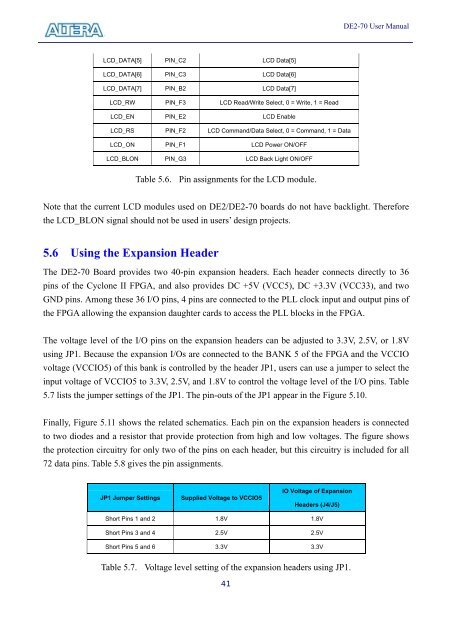
LCD_DATA[5] PIN_C2 LCD Data[5]<br />
LCD_DATA[6] PIN_C3 LCD Data[6]<br />
LCD_DATA[7] PIN_B2 LCD Data[7]<br />
LCD_RW PIN_F3 LCD Read/Write Select, 0 = Write, 1 = Read<br />
LCD_EN PIN_E2 LCD Enable<br />
LCD_RS PIN_F2 LCD Command/Data Select, 0 = Command, 1 = Data<br />
LCD_ON PIN_F1 LCD Power ON/OFF<br />
LCD_BLON PIN_G3 LCD Back Light ON/OFF<br />
Table 5.6. Pin assignments for the LCD module.<br />
41<br />
<strong>DE2</strong>-<strong>70</strong> User <strong>Manual</strong><br />
Note that the current LCD modules used on <strong>DE2</strong>/<strong>DE2</strong>-<strong>70</strong> boards do not have backlight. Therefore<br />
the LCD_BLON signal should not be used in users’ design projects.<br />
5.6 Using the Expansion Header<br />
The <strong>DE2</strong>-<strong>70</strong> Board provides two 40-pin expansion headers. Each header connects directly to 36<br />
pins of the Cyclone II FPGA, and also provides DC +5V (VCC5), DC +3.3V (VCC33), and two<br />
GND pins. Among these 36 I/O pins, 4 pins are connected to the PLL clock input and output pins of<br />
the FPGA allowing the expansion daughter cards to access the PLL blocks in the FPGA.<br />
The voltage level of the I/O pins on the expansion headers can be adjusted to 3.3V, 2.5V, or 1.8V<br />
using JP1. Because the expansion I/Os are connected to the BANK 5 of the FPGA and the VCCIO<br />
voltage (VCCIO5) of this bank is controlled by the header JP1, users can use a jumper to select the<br />
input voltage of VCCIO5 to 3.3V, 2.5V, and 1.8V to control the voltage level of the I/O pins. Table<br />
5.7 lists the jumper settings of the JP1. The pin-outs of the JP1 appear in the Figure 5.10.<br />
Finally, Figure 5.11 shows the related schematics. Each pin on the expansion headers is connected<br />
to two diodes and a resistor that provide protection from high and low voltages. The figure shows<br />
the protection circuitry for only two of the pins on each header, but this circuitry is included for all<br />
72 data pins. Table 5.8 gives the pin assignments.<br />
JP1 Jumper Settings Supplied Voltage to VCCIO5<br />
IO Voltage of Expansion<br />
Headers (J4/J5)<br />
Short Pins 1 and 2 1.8V 1.8V<br />
Short Pins 3 and 4 2.5V 2.5V<br />
Short Pins 5 and 6 3.3V 3.3V<br />
Table 5.7. Voltage level setting of the expansion headers using JP1.