DE2-70 Manual - Computation Structures Group
DE2-70 Manual - Computation Structures Group
DE2-70 Manual - Computation Structures Group

You also want an ePaper? Increase the reach of your titles
YUMPU automatically turns print PDFs into web optimized ePapers that Google loves.
5.7 Using VGA<br />
45<br />
<strong>DE2</strong>-<strong>70</strong> User <strong>Manual</strong><br />
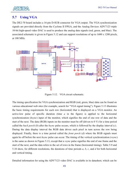
The <strong>DE2</strong>-<strong>70</strong> board includes a 16-pin D-SUB connector for VGA output. The VGA synchronization<br />
signals are provided directly from the Cyclone II FPGA, and the Analog Devices ADV7123 triple<br />
10-bit high-speed video DAC is used to produce the analog data signals (red, green, and blue). The<br />
associated schematic is given in Figure 5.12 and can support resolutions of up to 1600 x 1200 pixels,<br />
at 100 MHz.<br />
VGA_R[0..9]<br />
VGA_G[0..9]<br />
VGA_B[0..9]<br />
VGA_G0<br />
VGA_G1<br />
VGA_G2<br />
VGA_G3<br />
VGA_G4<br />
VGA_G5<br />
VGA_G6<br />
VGA_G7<br />
VGA_G8<br />
VGA_G9<br />
VGA_BLANK_n<br />
VGA_SYNC_n<br />
U10 U10<br />
1<br />
G0<br />
2<br />
G1<br />
3<br />
G2<br />
4<br />
G3<br />
7<br />
G6<br />
11<br />
BLANK<br />
12<br />
SYNC<br />
G9<br />
5<br />
G4<br />
6<br />
G5<br />
8<br />
G7<br />
9<br />
G8<br />
10<br />
VGA_R9<br />
VGA_R8<br />
VGA_R7<br />
VGA_R6<br />
VGA_R5<br />
VGA_R4<br />
VGA_R3<br />
VGA_R2<br />
VGA_R1<br />
VGA_R0<br />
48<br />
47<br />
46<br />
45<br />
44<br />
43<br />
42<br />
41<br />
40<br />
39<br />
38<br />
37<br />
R9<br />
R8<br />
R7<br />
R6<br />
R5<br />
R4<br />
R3<br />
R2<br />
R1<br />
R0<br />
PSAVE<br />
RSET<br />
VGA_B0<br />
VGA_B1<br />
VGA_B2<br />
VGA_B3<br />
VGA_B4<br />
VGA_B5<br />
VGA_B6<br />
VGA_B7<br />
VGA_B8<br />
VGA_B9<br />
VGA_CLOCK<br />
VGA_VCC33<br />
ADV7123 ADV7123<br />
VAA<br />
B0<br />
B1<br />
B2<br />
B3<br />
B4<br />
B5<br />
B6<br />
B7<br />
B8<br />
B9<br />
CLOCK<br />
13<br />
14<br />
15<br />
16<br />
17<br />
18<br />
19<br />
20<br />
21<br />
22<br />
23<br />
24<br />
R80 R80 4.7K 4.7K<br />
R81 R81 560 560<br />
RSET<br />
IOG<br />
VAA<br />
30<br />
VAA<br />
29<br />
IOB<br />
28<br />
IOB<br />
27<br />
GND<br />
26<br />
GND<br />
25<br />
31<br />
IOG 32<br />
VREF<br />
36<br />
COMP<br />
35<br />
IOR<br />
34<br />
IOR<br />
33<br />
VGA_VCC33<br />
VGA_VCC33<br />
BC47 BC47<br />
0.1u 0.1u<br />
BC48 BC48<br />
0.1u 0.1u<br />
R82 R82<br />
75 75<br />
R83 R83<br />
75 75<br />
R84 R84<br />
75 75<br />
VGA_HS<br />
VGA_VS<br />
Figure 5.12. VGA circuit schematic.<br />
VGA_R<br />
VGA_G<br />
VGA_B<br />
R85 R85 47 47<br />
R86 R86 47 47<br />
J7 J7<br />
1<br />
2<br />
3<br />
4<br />
5<br />
6<br />
7<br />
8<br />
9<br />
10<br />
11<br />
12<br />
13<br />
14<br />
15<br />
BC49 BC49 0.1u 0.1u<br />
16<br />
11<br />
66<br />
11 11<br />
10 10<br />
55 15 15<br />
The timing specification for VGA synchronization and RGB (red, green, blue) data can be found on<br />
various educational web sites (for example, search for “VGA signal timing”). Figure 5.13 illustrates<br />
the basic timing requirements for each row (horizontal) that is displayed on a VGA monitor. An<br />
active-low pulse of specific duration (time a in the figure) is applied to the horizontal<br />
synchronization (hsync) input of the monitor, which signifies the end of one row of data and the<br />
start of the next. The data (RGB) inputs on the monitor must be off (driven to 0 V) for a time period<br />
called the back porch (b) after the hsync pulse occurs, which is followed by the display interval (c).<br />
During the data display interval the RGB data drives each pixel in turn across the row being<br />
displayed. Finally, there is a time period called the front porch (d) where the RGB signals must<br />
again be off before the next hsync pulse can occur. The timing of the vertical synchronization (vsync)<br />
is the same as shown in Figure 5.13, except that a vsync pulse signifies the end of one frame and the<br />
start of the next, and the data refers to the set of rows in the frame (horizontal timing). Table 5.9 and<br />
5.10 show, for different resolutions, the durations of time periods a, b, c, and d for both horizontal<br />
and vertical timing.<br />
Detailed information for using the ADV7123 video DAC is available in its datasheet, which can be<br />
17<br />
VGA VGA