Explanation of Format - Smithsonian - The Chip Collection
Explanation of Format - Smithsonian - The Chip Collection
Explanation of Format - Smithsonian - The Chip Collection
Create successful ePaper yourself
Turn your PDF publications into a flip-book with our unique Google optimized e-Paper software.
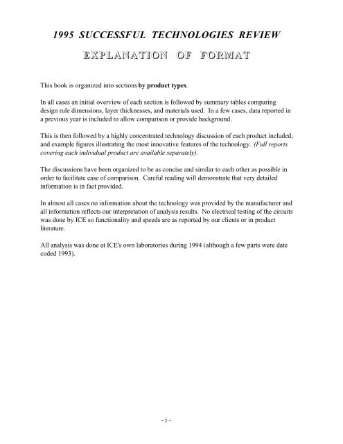
1995 SUCCESSFUL TECHNOLOGIES REVIEW<br />
EXPLANATION OF FORMAT<br />
This book is organized into sections by product types.<br />
In all cases an initial overview <strong>of</strong> each section is followed by summary tables comparing<br />
design rule dimensions, layer thicknesses, and materials used. In a few cases, data reported in<br />
a previous year is included to allow comparison or provide background.<br />
This is then followed by a highly concentrated technology discussion <strong>of</strong> each product included,<br />
and example figures illustrating the most innovative features <strong>of</strong> the technology. (Full reports<br />
covering each individual product are available separately).<br />
<strong>The</strong> discussions have been organized to be as concise and similar to each other as possible in<br />
order to facilitate ease <strong>of</strong> comparison. Careful reading will demonstrate that very detailed<br />
information is in fact provided.<br />
In almost all cases no information about the technology was provided by the manufacturer and<br />
all information reflects our interpretation <strong>of</strong> analysis results. No electrical testing <strong>of</strong> the circuits<br />
was done by ICE so functionality and speeds are as reported by our clients or in product<br />
literature.<br />
All analysis was done at ICE's own laboratories during 1994 (although a few parts were date<br />
coded 1993).<br />
- i -
OVERVIEW OF<br />
1994 TECHNOLOGY<br />
As usual, a number <strong>of</strong> interesting and in some cases at least, unexpected developments occurred<br />
during 1994.<br />
<strong>The</strong> most noticeable <strong>of</strong> these was in the DRAM area where we not only saw our first 64 Mb DRAMs,<br />
but also learned how slow they are in getting into production and how persistent the 16 Mb parts<br />
became. In fact, we found out that some manufacturers are now into their fourth 16 Mb design, a<br />
record as far as we know.<br />
In SRAMs the focus this last year seems to have shifted to byte-wide organizations like 64K x 18/16.<br />
Here also we have not seen a rush <strong>of</strong> activity into the 4 Mb designs although NEC's 64K x 18 does<br />
incorporate their 4 Mb cell design.<br />
Flash has not lost much impetus and showed interesting design features, namely that redesign <strong>of</strong> the<br />
cell is not necessary (or possible?). All one really needs to do to cram more bits into a package is to<br />
shrink dimensions and/or stack more than one die in a package (e.g., Intel 32 Mb). Based on this kind<br />
<strong>of</strong> pressure to reduce design rules, we would expect these parts to be at the leading edge in small<br />
features, but this has so far not been the case.<br />
<strong>The</strong> broad category <strong>of</strong> programable devices covering FPGAs, EPLAs, and EPLDs continue to<br />
represent mature technology with either a clever circuit design or a unique special process feature.<br />
<strong>The</strong>se include anything from anti-fuse to one-time programable UVEPROMs to EEPROMs, etc. No<br />
drastically new items were seen this year, but the normal process and design rule trends do result in<br />
dice with larger capacities or new circuit features.<br />
Microprocessors continue to be very active in pushing the technology, even more so than DRAMs.<br />
As pro<strong>of</strong> <strong>of</strong> this the minimum gate lengths observed (0.3 micron) this year were on the latest NEC<br />
MIPS design, the most metal levels on IBM and Intel entries, and the only evidence so far <strong>of</strong> shallow<br />
trench isolation, on the IBM parts. Also CMP planarization and use <strong>of</strong> plugs for vertical interconnect<br />
is more prevalent in this product category then elsewhere.<br />
Overall we observed the following trends.<br />
• Smaller dimensions <strong>of</strong> course, reaching 0.3 micron gate lengths (although 0.45 or 0.5<br />
micron is much more common). Also 0.5 micron metal widths and in a few cases,<br />
spacing.<br />
• Contacts in the 0.6 micron to 0.8 micron. DRAM cells less than 2 micron2 (1.6 micron<br />
minimum) and SRAM cells at 18 microns2 on dedicated SRAM parts, but very close<br />
(21 microns2 ) on CPUs.<br />
- ii -
• More levels <strong>of</strong> interconnect. Three or four (including metal substitute layers like<br />
polycides) are now becoming common and we have in fact seen six levels <strong>of</strong> metal.<br />
• Also more use <strong>of</strong> wells and implants and a slow trend towards more chemicalmechanical<br />
planarization (CMP).<br />
• Missing this year were larger dice. <strong>The</strong> largest seen being some 20 percent smaller than<br />
reported on last year.<br />
- iii -
TABLE OF MOST<br />
AGGRESSIVE FEATURE SIZES<br />
<strong>The</strong> following table shows the most aggressive features ICE observed in 1994.<br />
FEATURE SIZES PRODUCT<br />
Largest die 230mm2 Hitachi 64 Mb DRAM<br />
Min metal 4 width 1.3μm IBM 486 Blue Lightning<br />
Min metal 4 space 1.0μm IBM 486 Blue Lightning<br />
Min metal 3 width 0.4μm Hitachi 64 Mb DRAM<br />
Min metal 3 space 0.5μm Hitachi 64 Mb DRAM<br />
Min metal 2 width 0.4μm Hitachi 64 Mb DRAM<br />
Min metal 2 space 0.5μm Hitachi 64 Mb DRAM<br />
Min metal 1 width 0.3μm Hitachi 64 Mb DRAM<br />
Min metal 1 space 0.45μm Hitachi 64 Mb DRAM<br />
Min poly width (not as gate) 0.25μm Hitachi 64 Mb DRAM and<br />
Samsung 16 Mb DRAM<br />
Min via (metal to metal) 0.6μm Hitachi 16 Mb DRAM<br />
Min contact (metal to silicon) 0.6μm NEC VR4400MC, Intel P54C,<br />
IBM PC604, Hitachi 16 Mb DRAM,<br />
AMD16 Mb FLASH<br />
Min gate length N/P 0.3μm/0.3μm NEC VR4400MC<br />
Min DRAM cell size 1.6μm2 Hitachi 64 Mb DRAM<br />
Min SRAM cell size 18μm2 NEC 1 Mb SRAM<br />
Most levels <strong>of</strong> metal 4 IBM PC604/PC603/486 Blue<br />
Lightning, Intel PENTIUM<br />
Most levels <strong>of</strong> poly 4 Hitachi, Hyundai and Samsung 16 Mb<br />
DRAMs, NEC 1 Mb SRAM<br />
Rated (ICE) most complex process Intel P54C PENTIUM<br />
Rated (ICE) most advanced technology Hitachi 64 Mb DRAM/NEC VR4400MC<br />
- iv -
INDEX<br />
- v -<br />
Page<br />
<strong>Explanation</strong> <strong>of</strong> <strong>Format</strong> i<br />
Overview <strong>of</strong> 1994 Technology ii<br />
Table <strong>of</strong> Most Aggressive Feature Sizes iv<br />
Section 1 - DRAMS<br />
• Overview 1 - 1<br />
• Table 1-1 Horizontal Dimensions<br />
• Table 1-2 Vertical Dimensions<br />
• Table 1-3 Die Materials<br />
• Products<br />
- Hitachi/T.I. HM51W64800J-7 64 Mbit DRAM 1 - 3<br />
- Hitachi HM51W17400ALTS-7 16 Mbit DRAM 1 - 6<br />
- Hyundai HY5117400JC-70 16 Mbit DRAM 1 - 9<br />
- Samsung KM44C4100AJ-7 16 Mbit DRAM 1 - 12<br />
Section 2 - SRAMs<br />
• Overview 2 - 1<br />
• Table 2-1 Horizontal Dimensions<br />
• Table 2-2 Vertical Dimensions<br />
• Table 2-3 Die Materials<br />
• Products<br />
- Hitachi HM621864HJP-20 1 Mbit (64K x 18) SRAM 2 - 2<br />
- NEC μPD431018LE-15 1 Mbit (64K x 18) SRAM 2 - 5<br />
- Micron MT5C64K16A1DJ-12 1 Mbit (64K x 16) SRAM 2 - 8<br />
- Samsung KM6161002J-15 1 Mbit (64K x 16) SRAM 2 - 11<br />
Section 3 - FLASH<br />
• Overview 3 - 1<br />
• Table 3-1 Horizontal Dimensions<br />
• Table 3-2 Vertical Dimensions<br />
• Table 3-3 Die Materials<br />
• Products<br />
- Intel E28F016SA/DD28F032SA 16 Mbit/32 Mbit FLASH 3 - 2<br />
- AMD Am29F016-120EC 16 Mbit FLASH 3 - 6<br />
- AMD Am29F040-90EC 4 Mbit FLASH 3 - 9<br />
- Atmel AT29C040-12TC 4 Mbit FLASH 3 - 12<br />
- SST NH29EE010-150 1 Mbit FLASH 3 - 14
INDEX (continued)<br />
Section 4 - Programmable Devices<br />
• Overview 4 - 1<br />
• Table 4-1 Horizontal Dimensions<br />
• Table 4-2 Vertical Dimensions<br />
• Table 4-3 Die Materials<br />
• Products<br />
- Actel A1280A FPGA 4 - 2<br />
- AT&T ATT3020-70 FPGA 4 - 5<br />
- Altera EPM5128LC EPLD 4 - 7<br />
- Altera EPM7032 EPLD 4- 9<br />
- Lattice GAL22V10C EPLA 4 - 11<br />
- AMD PAL CE22V10H-5JC/5 EPLA 4 - 14<br />
Section 5 - Microprocessors<br />
• Overview 5 - 1<br />
• Table 5-1 Horizontal Dimensions<br />
• Table 5-2 Vertical Dimensions<br />
• Table 5-3 Die Materials<br />
• Products<br />
- NEC VR4400MC 64-bit CPU (RISC) 5 - 2<br />
- IDT 79R4600-100G "ORION" 64-bit CPU (RISC) 5 - 5<br />
- Intel P54C "PENTIUM" 64-bit CPU (CISC) 5 - 8<br />
- IBM/Motorola PC604 (and PC603) 64-bit CPU (RISC) 5 - 11<br />
- IBM 486 Blue Lightning 32-bit CPU (CISC) 5 - 14<br />
- vi -


