Chapter 2. COST PER WAFER - Smithsonian - The Chip Collection
Chapter 2. COST PER WAFER - Smithsonian - The Chip Collection
Chapter 2. COST PER WAFER - Smithsonian - The Chip Collection

Create successful ePaper yourself
Turn your PDF publications into a flip-book with our unique Google optimized e-Paper software.
2<br />
Cost Per Wafer
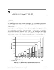
2 Cost Per Wafer<br />
Cost per wafer is perhaps the most widely<br />
used cost metric in the semiconductor industry.<br />
Its value lies in the ability to combine<br />
large quantities of cost data and obtain one<br />
indicator of operating cost that can be used to<br />
compare different pieces of equipment, different<br />
processes, alternative materials, etc. Cost<br />
per wafer can also be used as a benchmarking<br />
metric (see <strong>Chapter</strong> 4, Fab Benchmarking). It<br />
can further be used to estimate a fair price for<br />
foundry-produced wafers.<br />
Information from the Semiconductor<br />
Industry Association in the U.S. indicates<br />
that average cost per wafer has increased by<br />
3X over the last 15 years (Figure 2-1).<br />
Although the cost of labor, materials and<br />
capital expenditures per wafer have<br />
increased, the real cost of manufacturing<br />
semiconductor chips continues to decrease<br />
because the number of transistors that can be<br />
placed on a wafer has grown faster than<br />
manufacturing costs, as shown in Figure 2-<strong>2.</strong><br />
As discussed in <strong>Chapter</strong> 1, this ever-increasing<br />
cost per wafer is offset by the ability to<br />
shrink feature size by 30 percent each<br />
device generation, thereby decreasing the<br />
manufacturing cost per transistor. <strong>The</strong><br />
effective price of DRAMs, measured in cost<br />
per bit, falls by 30 percent per year. Rising<br />
manufacturing cost is further offset by manufacturersÕ<br />
ability to continually increase<br />
device yields, transition to larger wafers<br />
sizes and increase the productivity of fab<br />
equipment and operations. By continually<br />
decreasing or controlling cost per wafer, IC<br />
manufacturers can increase profitability.<br />
Cost per wafer at the fab level can be simply<br />
computed using the total cost of manufacturing<br />
divided by the total number of yielded<br />
wafers produced. Cost per wafer at the<br />
equipment level is typically computed Òfrom<br />
the ground-upÓ using the cost of equipment<br />
depreciation, cost of direct labor, maintenance<br />
and materials, cost of energy and other<br />
facilities as well as building depreciation<br />
costs.<br />
Cost per wafer first enjoyed widespread use<br />
several years following the introduction of<br />
cost-of-ownership modeling by SEMAT-<br />
ECH, the consortium of semiconductor manufacturers<br />
in the U.S. Cost per wafer is often<br />
used to compare the cost-of-ownership performance<br />
of competing pieces of equipment.<br />
It is also used by semiconductor manufacturers<br />
for benchmarking purposes, and to<br />
assess the cost of making process modifications<br />
and adopting new processes.<br />
Importantly, however, one of the most critical<br />
components in cost-of-ownership calculations<br />
is the yield of the given process step.<br />
Because yield influences cost so dramatically<br />
and because yield is very difficult to determine<br />
on a step-by-step basis, most COO calculations<br />
assume identical yields from one<br />
process tool to another. For more discussion<br />
on COO see <strong>Chapter</strong> 4, Fab Benchmarking.<br />
INTEGRATED CIRCUIT ENGINEERING CORPORATION 2-1
Cost Per Wafer<br />
R&D = $74<br />
(10.1%)<br />
2-2<br />
S, G&A = $158<br />
(21.6%)<br />
Non-Labor<br />
Mfg = $157<br />
(21.5%)<br />
Mfg Cost of<br />
Goods Sold = $432<br />
(59.1%)<br />
R&D = $257<br />
(10.8%)<br />
S, G&A = $374<br />
(15.8%)<br />
Non-Labor<br />
Mfg = $994<br />
(41.9%)<br />
Depreciation = $247<br />
(10.4%)<br />
Depreciation = $67<br />
(9.2%) Mfg Labor = $275<br />
(37.6%)<br />
Taxes &<br />
Other = $230<br />
(9.7%)<br />
Mfg Labor = $273<br />
(11.5%)<br />
1980<br />
1995<br />
Total = $731/150mm Wafer<br />
*North American firms only<br />
Total = $2,375/150mm Wafer<br />
Source: SIA<br />
Index (1982 = 100)<br />
1,000<br />
100<br />
10<br />
1<br />
Figure 2-1. Total Cost Per Wafer Start (1980 Versus 1995*)<br />
Manufacturing<br />
Cost Per Wafer<br />
DRAM<br />
Price Per Bit<br />
1982 1983 1984 1985 1986 1987 1988 1989 1990 1991 1992 1993 1994 1995<br />
Figure 2-<strong>2.</strong> How Decreasing Cost Per Bit Compensates for Increasing Manufacturing Cost<br />
Mfg Cost of<br />
Goods Sold = $1,268<br />
(53.4%)<br />
Year<br />
Source: SIA 22726<br />
21075A<br />
INTEGRATED CIRCUIT ENGINEERING CORPORATION
Operating Costs<br />
Fab operating costs can be divided into fixed<br />
costs and variable costs. Fixed costs include<br />
equipment depreciation, R&D, overhead,<br />
and general and administrative costs. <strong>The</strong><br />
most important variable cost is the cost of<br />
sales (manufacturing cost of goods sold),<br />
which includes the cost of consumables,<br />
spare parts, materials (including cleanroom<br />
garments, etc.), labor, production control,<br />
and facilities (operating power for the plant,<br />
deionized water systems, etc.). <strong>The</strong> trend of<br />
increasing manufacturing cost of goods sold<br />
is shown in Figure 2-3. This cost of manufacturing<br />
wafers, without considering<br />
increasing depreciation costs, rises at an<br />
average rate of 5-6 percent per year.<br />
150mm Equivalent Wafer<br />
1,300<br />
1,200<br />
1,100<br />
1,000<br />
900<br />
800<br />
700<br />
600<br />
500<br />
400<br />
Mean<br />
Cost Per Wafer<br />
Operating costs are often defined for wafer<br />
processing alone as assembly and final testing<br />
of devices are commonly performed at a<br />
different manufacturing sites, often in<br />
Southeast Asian countries where labor costs<br />
are low by North American, Japanese, and<br />
European standards. In rough terms, IC<br />
manufacturing costs can be divided into<br />
three categories consisting of:<br />
¥ 10-15 percent due to labor cost,<br />
¥ 35-40 percent due to materials costs<br />
(including starting wafer cost), and<br />
¥ 40-50 percent for capital costs [1]<br />
Annual Trend<br />
Growth = 5.6%<br />
1978 1979 1980 1981 1982 1983 1984 1985 1986 1987 1988 1989 1990 1991 1992 1993 1994 1995<br />
Source: SIA 22727<br />
Figure 2-3. Manufacturing Cost of Goods Sold (Less Depreciation) Per Wafer Start<br />
INTEGRATED CIRCUIT ENGINEERING CORPORATION 2-3
Cost Per Wafer<br />
Beyond these broad categories, operating<br />
costs are typically broken down into four<br />
main components:<br />
¥ Manufacturing cost of devices sold (all<br />
costs directly allocated to production, less<br />
depreciation),<br />
¥ Selling, general and administrative<br />
expenses,<br />
¥ Research and development costs, and<br />
¥ Depreciation expenses.<br />
As shown in Figure 2-1, manufacturing cost<br />
of goods sold in 1995 accounted for over 53<br />
percent of the total cost per wafer start for<br />
merchant IC producers in the U.S. [2] Cost per<br />
wafer for IC manufacturers has increased<br />
from 1980Õs level of around $730 per 150mm<br />
equivalent wafer to 1995Õs level of nearly<br />
$2,400 per 150mm wafer. In other words, the<br />
cost per wafer has risen by over a factor of<br />
three in a fifteen year period. In addition, the<br />
portion of manufacturing costs due to labor<br />
expenses has dropped dramatically.<br />
Interestingly, the dollar amount companies<br />
had to devote to labor was almost exactly the<br />
same in 1995 as it was in 1980.<br />
<strong>The</strong>se expenditures can also be viewed relative<br />
to annual semiconductor industry sales.<br />
In other words, the rates of increase in<br />
expenditures for manufacturing, R&D,<br />
depreciation, and S, G&A expenses can be<br />
compared to the rate of annual increases in<br />
overall semiconductor industry revenues.<br />
Shown in Figure 2-4 are year-to-year values<br />
for R&D, depreciation expenses, manufacturing<br />
costs, S, G&A costs, and semiconductor<br />
sales, normalized to 1978 values. Long<br />
term, depreciation and R&D costs have risen<br />
much more dramatically than manufacturing<br />
costs, semiconductor sales, and S, G&A<br />
expenditures. Between 1978 and 1995,<br />
depreciation outlays increased by a factor of<br />
17; R&D costs increased by a factor of 14;<br />
2-4<br />
manufacturing costs and S, G&A costs<br />
increased by almost a factor of 9 each; and<br />
sales by U.S.-based merchant semiconductor<br />
firms increased by a factor of 1<strong>2.</strong> As can be<br />
gleaned from this illustration, during the<br />
industryÕs most difficult period in the mid-<br />
1980s, R&D and depreciation expenditures<br />
remained high while the sales index (annual<br />
semiconductor sales) dipped too low to support<br />
these expenditures.<br />
In the most recent expansionary cycle<br />
between 1993 and 1996, the focus on increasing<br />
expenditures for equipment and new<br />
fabs has increased dramatically. However, as<br />
shown in Figure 2-5, depreciation expenses<br />
as a percent of sales appear to be stabilizing,<br />
despite a long-term average increase of 10-15<br />
percent per year.<br />
<strong>The</strong> following sections briefly discusses the<br />
cost components for manufacturing costs,<br />
depreciation, and R&D costs. Selling, general<br />
and administrative costs will not be covered<br />
as these expenditures vary a great deal<br />
from one company to the next, and vary little<br />
from year to year for a given company.<br />
R&D and Depreciation Costs<br />
As mentioned previously, due to the<br />
extremely high pace of technological innovation<br />
in this industry, necessary investment<br />
for R&D, new fabs, and equipment can be as<br />
high as 25-30 percent of sales. In fact, the<br />
percentage of sales that must be reinvested<br />
for R&D in the semiconductor industry surpasses<br />
that needed in nearly every other<br />
high technology industry (Figure 2-6).<br />
Interestingly enough, the key industries that<br />
semiconductors feedÑcomputers, consumer<br />
electronics, communications, and automotiveÑeach<br />
requires lower investment to<br />
develop than the chips that run them.<br />
INTEGRATED CIRCUIT ENGINEERING CORPORATION
Index: 1978 =- 1.0<br />
18.0<br />
17.0<br />
16.0<br />
15.0<br />
14.0<br />
13.0<br />
1<strong>2.</strong>0<br />
11.0<br />
10.0<br />
9.0<br />
8.0<br />
7.0<br />
6.0<br />
5.0<br />
4.0<br />
3.0<br />
<strong>2.</strong>0<br />
Mfg. Cost of<br />
Goods Sold<br />
S, G&A<br />
Depreciation<br />
R&D<br />
Sales Index<br />
1.0<br />
1978 1979 1980 1981 1982 1983 1984 1985 1986 1987 1988 1989 1990 1991 1992 1993 1994 1995<br />
Year<br />
Note: U.S. merchant semiconductor manufacturers only.<br />
Source: SIA 19783B<br />
Depreciation as a Percent of Sales Revenue<br />
16<br />
14<br />
12<br />
10<br />
8<br />
6<br />
Figure 2-4. Annual Expenditures for Major Cost Components<br />
4<br />
1978 1979 1980 1981 1982 1983 1984 1985 1986 1987 1988 1989 1990 1991 1992 1993 1994 1995<br />
Note: U.S. merchant semiconductor manufacturers only.<br />
Source: SIA<br />
Cost Per Wafer<br />
INTEGRATED CIRCUIT ENGINEERING CORPORATION 2-5<br />
Year<br />
Median<br />
Mean<br />
Figure 2-5. Depreciation Expenses Rise More Rapidly Than IC Revenues<br />
19784B
Cost Per Wafer<br />
In addition, as technology development<br />
becomes more expensive, it becomes more<br />
difficult to get a timely return on investment.<br />
Generally, IC manufacturers invest 10-15<br />
percent of sales each year in R&D. Figure 2-<br />
7 shows R&D expenditures both in billions<br />
of dollars and as a percentage of sales revenues<br />
for merchant IC manufacturers in the<br />
US. While this percentage appears to have<br />
declined over the 1992-1995 period, R&D<br />
outlays rose dramatically at an average<br />
annual rate of 18 percent over the period.<br />
2-6<br />
Software and Services<br />
Semiconductors,,,,,,,,,,,,,,,,,,<br />
,,,,,,,,,,,,,,,,,,<br />
,,,,,,,,,,,,,,,,,,<br />
Computer Communications<br />
Office Equipment<br />
(Excluding Computers)<br />
Aerospace and Defense<br />
Chemicals<br />
Automotive<br />
Telecommunications<br />
General Manufacturing<br />
Electrical Products<br />
Source: Business Week<br />
Health Care<br />
Computers<br />
Electronics<br />
Instruments<br />
0 2 4 6 8 10 12 14<br />
R&D as a Percent of Sales<br />
19781A<br />
Figure 2-6. R&D For Semiconductors Exceed Most Other High Technology Industries<br />
<strong>The</strong> most important components in development<br />
costs are equipment costs and labor, as<br />
illustrated in Figure 2-8. One of the most<br />
important strategies used by semiconductor<br />
companies to control these costs is the formation<br />
of strategic partnerships for both<br />
technology development and in some cases,<br />
fab ownership.<br />
Also shown back in <strong>Chapter</strong> 1, the top 10<br />
companies accounted for 55 percent of all<br />
capital spending in the semiconductor<br />
INTEGRATED CIRCUIT ENGINEERING CORPORATION
industry in 1996, and 83 percent of all spending<br />
is performed by 25 companies.<br />
Worldwide, SEMI and SEAJ estimate that<br />
63.5 percent of capital spending goes toward<br />
wafer processing equipment, 21 percent<br />
toward testing equipment, nearly 10 percent<br />
to assembly equipment and nearly 6 percent<br />
Billions of Dollars<br />
6.0<br />
5.5<br />
5.0<br />
4.5<br />
4.0<br />
3.5<br />
3.0<br />
<strong>2.</strong>5<br />
<strong>2.</strong>0<br />
1.5<br />
1.0<br />
0.5<br />
0.0<br />
Percentage of Sales<br />
1978 1979 1980 1981 1982 1983 1984 1985<br />
Annual Trend<br />
Growth = 14.7%<br />
1986 1987<br />
Year<br />
Cost Per Wafer<br />
to facility related equipment (i.e., computers,<br />
automation, etc.). <strong>The</strong>se numbers equate to<br />
1996 market sizes of $26.6 billion for wafer<br />
processing equipment, $8.8 billion for testing<br />
equipment, $4 billion for assembly equipment<br />
and $<strong>2.</strong>5 billion for facility equipment.<br />
Billions of Dollars<br />
1988 1989 1990 1991 1992 1993 1994 1995<br />
Source: SIA 22728<br />
Figure 2-7. Semiconductor R&D Expenditures<br />
Consumables<br />
(Gases and Chemicals)<br />
16%<br />
Facilities and Property<br />
19%<br />
Source: Intel/EE Times<br />
Other (Including Travel)<br />
8%<br />
Labor 26%<br />
Equipment<br />
31%<br />
INTEGRATED CIRCUIT ENGINEERING CORPORATION 2-7<br />
19977A<br />
Figure 2-8. Breakdown of Semiconductor Technology Development Costs<br />
18.0<br />
16.0<br />
14.0<br />
1<strong>2.</strong>0<br />
10.0<br />
8.0<br />
6.0<br />
Percent of Sales Revenues
Cost Per Wafer<br />
Depreciation schedules vary from one country<br />
to another. Semiconductor firms in the<br />
U.S. have attempted to change 5-year depreciation<br />
schedules on semiconductor processing<br />
equipment to 3 years to better reflect the<br />
rapid rate of technological obsolescence in<br />
fabs today. Despite bipartisan support in the<br />
U.S. House of Representatives and Senate,<br />
the bill to change these depreciation schedules<br />
did not pass. However, some progress<br />
was made in 1997 as a bill was passed to<br />
raise R&D tax credit for basic research from 8<br />
percent to 11 percent. <strong>The</strong> bill also allows a 6<br />
percent manufacturers investment credit for<br />
cleanrooms built by IC manufacturers and<br />
semiconductor equipment companies.<br />
Figure 2-9 shows depreciation schedules for<br />
a fab facility in the U.S.<br />
2-8<br />
Year in<br />
Service Land<br />
1<br />
2<br />
3<br />
4<br />
5<br />
6<br />
7<br />
8<br />
9<br />
10<br />
11<br />
12<br />
13<br />
14<br />
15<br />
16<br />
100%<br />
104%<br />
108%<br />
112%<br />
117%<br />
122%<br />
127%<br />
132%<br />
137%<br />
142%<br />
148%<br />
154%<br />
160%<br />
167%<br />
173%<br />
180%<br />
Fab<br />
Building<br />
98%<br />
97%<br />
97%<br />
97%<br />
97%<br />
96%<br />
95%<br />
94%<br />
93%<br />
91%<br />
90%<br />
89%<br />
87%<br />
85%<br />
83%<br />
81%<br />
Cleanroom<br />
Equipment<br />
89%<br />
79%<br />
70%<br />
62%<br />
55%<br />
49%<br />
44%<br />
39%<br />
35%<br />
31%<br />
28%<br />
25%<br />
22%<br />
20%<br />
20%<br />
20%<br />
Source: Oregon Department of Revenue 1994-1995 Electronics<br />
Trend and Depreciation Schedules<br />
Within the fab area, the photolithography<br />
cell is the most expensive (Figure 2-10), as<br />
leading-edge steppers and step-and-scan<br />
machines for 0.25um processing are priced<br />
between $5-$7 million each. In addition, the<br />
investment for advanced reticles is rising<br />
rapidly (Figure 2-11). Beyond lithography<br />
costs, the next most expensive is diffusion<br />
processes, followed by etching, thin film<br />
deposition, and ion implantation. Trends<br />
indicate a long-term increase in number of<br />
CVD, sputtering, and etching tools in the fab,<br />
principally driven by an increasing number<br />
of metal layers in advanced logic devices<br />
(currently at 5-6 levels for 64-bit MPUs), and<br />
the introduction of chemical mechanical polishing<br />
tools for global planarization. Many<br />
sources estimate that back-end wafer processing<br />
(all processing of films above the<br />
substrate level) accounts for more than 50<br />
percent of overall cost per wafer.<br />
Wafer<br />
Processing<br />
Equipment<br />
67%<br />
46%<br />
29%<br />
16%<br />
10%<br />
10%<br />
10%<br />
10%<br />
10%<br />
10%<br />
10%<br />
10%<br />
10%<br />
10%<br />
10%<br />
10%<br />
Office<br />
and Utility<br />
98%<br />
94%<br />
90%<br />
86%<br />
82%<br />
79%<br />
76%<br />
74%<br />
72%<br />
69%<br />
67%<br />
65%<br />
64%<br />
62%<br />
61%<br />
60%<br />
Figure 2-9. Depreciation Schedules Projected Appraised Value of Investment<br />
as Percentage of Original Cost<br />
22729<br />
INTEGRATED CIRCUIT ENGINEERING CORPORATION
Thin Films<br />
16%<br />
Etch<br />
18%<br />
Implant<br />
12%<br />
Long-term increases in depreciation and<br />
R&D expenditures continually challenge the<br />
cost-effectiveness of IC manufacturing. One<br />
metric used to examine overall cost effectiveness<br />
is asset turnover rate. Figure 2-12<br />
shows that in the years preceding 1980,<br />
every dollar of net fixed assets generated<br />
greater than $3.00 in sales revenue. By 1987,<br />
asset turnover rate had fallen by 50 percent.<br />
However, recent trends indicate that asset<br />
Photolithography<br />
32%<br />
Diffusion<br />
22%<br />
Source: Microlithography World 21070<br />
Figure 2-10. Relative Costs of Semiconductor Manufacturing Areas<br />
Billions of Dollars<br />
1,000<br />
100<br />
10<br />
1<br />
Semiconductor Market<br />
Mask Market<br />
0.1<br />
1977 1980 1985 1990 1995 2000<br />
Year<br />
Source: Wafer News/Rose Assoc. 22693<br />
Figure 2-11. Growing Investment in Reticles and Masks<br />
Cost Per Wafer<br />
turnover rates are stabilizing. However, further<br />
deterioration in the rate may affect the<br />
financial future of the industry. Once again,<br />
by making facilities and operations more<br />
cost effective, margins can be preserved and<br />
the rate of technological advancement can<br />
continue at its rapid pace. Astoundingly, the<br />
average employee of a merchant IC manufacturer<br />
in the U.S. is supported by $120,000<br />
in net fixed assets (Figure 2-13).<br />
INTEGRATED CIRCUIT ENGINEERING CORPORATION 2-9
Cost Per Wafer<br />
2-10<br />
Net Fixed Assets/Sales ($)<br />
4.0<br />
3.5<br />
3.0<br />
<strong>2.</strong>5<br />
<strong>2.</strong>0<br />
1.5<br />
1978 1979 1980 1981 1982 1983 1984 1985 1986 1987 1988 1989 1990 1991 1992 1993 1994 1995<br />
Source: SIA 22730<br />
$1,000 Per Employee<br />
140<br />
120<br />
100<br />
80<br />
60<br />
40<br />
20<br />
0<br />
Mean<br />
Median<br />
Year<br />
Figure 2-1<strong>2.</strong> Net Fixed Assets Rise Faster Than Industry Revenues<br />
Median<br />
Mean<br />
1978 1979 1980 1981 1982 1983 1984 1985 1986 1987 1988 1989 1990 1991 1992 1993 1994 1995<br />
Year<br />
Source: SIA 22731<br />
Figure 2-13. Net Fixed Assets Per Employee<br />
INTEGRATED CIRCUIT ENGINEERING CORPORATION
<strong>The</strong> Cost of Labor<br />
As semiconductor fabs become more automated<br />
and reliable, labor costs typically represent<br />
a smaller portion of total wafer<br />
processing costs. As shown back in Figure 2-<br />
1, total labor costs typically constitute 11.5<br />
percent of overall cost per wafer for U.S.<br />
firms. Figure 2-14 shows how the total labor<br />
rate (including wages, salaries, payroll taxes,<br />
etc.) as a percent of sales for U.S. firms has<br />
dropped dramatically over the last several<br />
years and the divergence between the mean<br />
and median lines indicates that larger firms<br />
spend much less on labor than smaller IC<br />
manufacturers, which is expected. Figure 2-<br />
15 gives a sampling of salaries and wages<br />
earned by different individuals working in<br />
or around the fab.<br />
Percent of Sales Revenues<br />
50<br />
45<br />
40<br />
35<br />
30<br />
25<br />
20<br />
Cost Per Wafer<br />
By 1996, labor rate differences between the<br />
U.S. and Japan had diminished due to<br />
changing standards in Japan and the changing<br />
value of the yen (Figure 2-16). <strong>The</strong><br />
semiconductor industry has become a truly<br />
global industry with fabs now emerging in<br />
all regions of the world. Regions that have<br />
recently attracted fabs include China,<br />
Malaysia, Thailand, India, and Eastern<br />
Europe. <strong>The</strong>se countries offer the labor cost<br />
advantages that Japan once enjoyed over<br />
the U.S. It comes as no surprise that these<br />
regions, home to many assembly houses,<br />
are now being used for wafer processing.<br />
Such developing regions offer enormous<br />
growth potential, as evidenced in the<br />
growth of exports in developing regions relative<br />
to export growth in developed regions<br />
(Figure 2-17).<br />
Median<br />
1978 1979 1980 1981 1982 1983 1984 1985 1986 1987 1988 1989 1990 1991 1992 1993 1994<br />
Year<br />
INTEGRATED CIRCUIT ENGINEERING CORPORATION 2-11<br />
Mean<br />
*Includes wages, salaries, retirement expenses, incentive compensation, payroll taxes<br />
**North American firms only<br />
Source: SIA 21072<br />
Figure 2-14. Total Labor Expenses* as a Percent of Sales Revenues**
Cost Per Wafer<br />
2-12<br />
Semiconductor (Dollars/Hour)<br />
Operator Wafer Fab I<br />
Operator Wafer Fab II<br />
Operator Wafer Fab III<br />
Semiconductor Specialist<br />
Semiconductor Line Mech.<br />
Semiconductor (Thousands of Dollars/Year)<br />
Process Engineer I<br />
Process Engineer II<br />
Process Engineer III<br />
Process Technician<br />
Sr. Process Technician<br />
QA Technician I<br />
QA Technician II<br />
QA Technician III<br />
QA Engineer<br />
Elec. Management (Thousands of Dollars/Year)<br />
Process Development Manager<br />
QA Manager<br />
MIS Manager<br />
R & D Manager<br />
HR Manager<br />
Compensation Manager<br />
Emp. Relations Manager<br />
Gen. Accounting Manager<br />
Facilities Manager<br />
Office Manager<br />
Production Manager<br />
Other Technical (Thousands of Dollars/Year)<br />
Test Engineer<br />
CAD Operator I<br />
Clerical (Thousands of Dollars/Year)<br />
Accounting Clerk I<br />
Receptionist<br />
Secretary<br />
Executive Secretary<br />
Administrative Assistant<br />
Data Entry Operator<br />
Minimum<br />
50th<br />
Percentile<br />
6.30<br />
7.24<br />
8.24<br />
9.49<br />
13.72<br />
30.8<br />
35.8<br />
44.3<br />
20.3<br />
25.5<br />
18.2<br />
20.6<br />
24.3<br />
33.8<br />
53.6<br />
47.4<br />
49.6<br />
60.1<br />
43.6<br />
47.4<br />
50.4<br />
43.4<br />
43.2<br />
31.0<br />
41.1<br />
34.5<br />
20.5<br />
15.7<br />
16.6<br />
21.5<br />
24.9<br />
24.8<br />
17.0<br />
Maximum<br />
Average<br />
9.98<br />
10.55<br />
1<strong>2.</strong>69<br />
14.78<br />
19.72<br />
47.5<br />
56.1<br />
68.7<br />
31.4<br />
38.7<br />
27.1<br />
30.9<br />
36.7<br />
51.0<br />
81.6<br />
74.4<br />
78.4<br />
94.8<br />
68.2<br />
71.6<br />
80.8<br />
68.2<br />
68.6<br />
47.4<br />
64.7<br />
5<strong>2.</strong>8<br />
30.5<br />
23.4<br />
23.9<br />
31.6<br />
36.9<br />
37.3<br />
24.3<br />
Definitions – Minimum 50th Percentile: <strong>The</strong> minimum salary range which<br />
is higher than 50% of all minimum ranges.<br />
Maximum Average: <strong>The</strong> average of the maximum<br />
salary ranges reported.<br />
Source: American Electronics Assoc.<br />
21076<br />
Figure 2-15. Typical Industry Salary Ranges in U.S., West Coast<br />
INTEGRATED CIRCUIT ENGINEERING CORPORATION
<strong>COST</strong><br />
FACTOR<br />
HOURLY RATE<br />
FRINGE RATE<br />
TOTAL<br />
LABOR <strong>COST</strong> <strong>PER</strong><br />
<strong>WAFER</strong> TO PROBE<br />
(1.5 HOURS)<br />
* 205 ¥ = $1.00<br />
**108¥ = $1.00<br />
Source: ICE<br />
1996<br />
U.S. <strong>WAFER</strong> FAB<br />
DIRECT LABOR RATE<br />
$11.80<br />
35%<br />
$15.93<br />
$23.90<br />
JAPANESE <strong>WAFER</strong> FAB DIRECT<br />
LABOR RATE<br />
1985 - 1986* 1996**<br />
Cost Per Wafer<br />
INTEGRATED CIRCUIT ENGINEERING CORPORATION 2-13<br />
$5.50<br />
40%<br />
$7.70<br />
$11.55<br />
$11.21<br />
40%<br />
$15.69<br />
$23.54<br />
12030J<br />
Figure 2-16. U.S. and Japanese 1995 IC Facility Direct Labor Costs<br />
Percentage of Exports<br />
220<br />
200<br />
180<br />
160<br />
140<br />
120<br />
100<br />
80<br />
60<br />
40<br />
20<br />
0<br />
217.1<br />
Developing<br />
Economies<br />
94.2<br />
World<br />
69.6<br />
Industrialized<br />
Economies<br />
Source: Wall Street Journal/DRI/McGraw Hill 22701<br />
Figure 2-17. Real Growth of Exports in the World, 1995-1996
Employees (Thousands)<br />
Cost Per Wafer<br />
Worldwide, the semiconductor industry<br />
employs roughly between 750,000 and a million<br />
people (Figure 2-18). Of these, approximately<br />
260,000 are employed by North<br />
American merchant semiconductor manufacturers.<br />
Figure 2-19 shows the cyclical patterns<br />
in North American on-shore and<br />
off-shore employment levels in response to<br />
changing market condition. As shown,<br />
employment levels have increased significantly<br />
between 1992 and 1995, despite continual<br />
advances in labor productivity. In<br />
1995, approximately 70 percent of the North<br />
American wages were disbursed to employees<br />
in North America, and the off-shore<br />
employee earns approximately one-third the<br />
salary of the employee based in North<br />
America, reflecting the semi-skilled labor at<br />
off-shore assembly operations as opposed to<br />
the base of highly-skilled and professional<br />
workers at North American facilities. This<br />
pay differential is narrowing slowly (Figure<br />
2-20) as off-shore wages steadily increase.<br />
2-14<br />
1,200<br />
1,000<br />
800<br />
600<br />
400<br />
200<br />
0<br />
520 510<br />
1987<br />
* Projected<br />
1990<br />
Year<br />
725<br />
1995<br />
2000*<br />
Source: Electronic Business Today 22689<br />
Figure 2-18. Worldwide Semiconductor<br />
Employment<br />
1,100<br />
Device Cost Modeling<br />
Several years ago ICE developed a simplified<br />
cost model to examine manufacturing costs.<br />
<strong>The</strong> model estimate a company's gross<br />
margin and revenues for a given device<br />
based on the ASP for the devices at the time,<br />
and a calculation of device factory cost based<br />
on design rules, type of device, equipment<br />
cost, wafer size used, defect density estimates,<br />
etc. Among these assumptions, defect<br />
density is the most critical. Through fab<br />
benchmarking studies and cost modeling,<br />
ICE developed the wafer cost estimates<br />
shown in Figure 2-21.<br />
Figures 2-22 and 2-23 show cost model<br />
results for a Pentium microprocessor and<br />
16M and 64M DRAM devices in first quarter<br />
1997. As shown, the advanced-generation<br />
Pentium device yields a significant gross<br />
margin as little competition exists in this<br />
marketplace. As the advanced-generation<br />
Pentiums mature and are replaced by the<br />
Pentium Pro device, Intel will continue to<br />
lower the price of this processor more dramatically<br />
and improve yields more quickly<br />
to preserve margins.<br />
<strong>The</strong> margins on DRAM devices, however,<br />
have dramatically declined in the past year,<br />
forcing important changes in the 16M<br />
DRAM market and the adoption of 64M<br />
technology. At least some DRAM manufacturers<br />
are accelerating their transition to 64M<br />
production due to the slim profit margins of<br />
16M devices, as illustrated in Figure 2-23. At<br />
the same time, manufacturers are rapidly<br />
shrinking the die size of 16M devices from<br />
typical levels of 80mm2 to as small as 60mm2<br />
to preserve yields and margins.<br />
INTEGRATED CIRCUIT ENGINEERING CORPORATION
1,000 Employees<br />
150<br />
140<br />
130<br />
120<br />
110<br />
100<br />
90<br />
1978<br />
1979<br />
1980<br />
1981<br />
1982<br />
1983<br />
1984<br />
1985<br />
Cost Per Wafer<br />
INTEGRATED CIRCUIT ENGINEERING CORPORATION 2-15<br />
1986<br />
Source: SIA 22732<br />
$1,000 Per Employee<br />
70<br />
60<br />
50<br />
40<br />
30<br />
20<br />
10<br />
0<br />
North America<br />
Offshore<br />
Year<br />
1987<br />
1988<br />
1989<br />
1990<br />
1991<br />
Figure 2-19. North America and Offshore Employment Levels<br />
North American<br />
Worldwide Average<br />
1978 1979 1980 1981 1982 1983 1984 1985 1986 1987 1988 1989 1990 1991 1992 1993 1994 1995<br />
Source: SIA 22733<br />
Year<br />
Figure 2-20. Labor Expenses Per Employee<br />
1992<br />
Annual Growth<br />
Trend = 10.8%<br />
Offshore<br />
1993<br />
1994<br />
1995
Cost Per Wafer<br />
DRAM, MPU and ASIC Manufacturing<br />
Costs<br />
<strong>The</strong> semiconductor industry has traditionally<br />
been driven by the needs of the DRAM<br />
manufacturers because these companies are<br />
the single largest consumers of semiconductor<br />
equipment and materials, and because<br />
DRAM devices, until recently, were the technology<br />
drivers. In recent years, microprocessors<br />
have become the technology driver as<br />
Intel has speeded its transitions to smaller<br />
feature sizes faster than the transitions in the<br />
2-16<br />
Feature<br />
Size (µm)<br />
1.5<br />
1.0<br />
0.8<br />
0.5<br />
0.35<br />
Source: ICE<br />
Wafer<br />
Size (mm) CMOS<br />
14-16 Masks<br />
125<br />
125/150<br />
150/200<br />
150/200<br />
200<br />
170<br />
—/310<br />
390/—<br />
525/—<br />
—<br />
Advanced<br />
CMOS<br />
18-20 Masks<br />
—<br />
—<br />
600/990<br />
700/1,140<br />
1,415<br />
Process Technology<br />
Advanced<br />
BiCMOS<br />
22 Masks<br />
360<br />
—/575<br />
660/ —<br />
900/1,400<br />
1,800<br />
Bipolar<br />
8-10 Masks<br />
210<br />
—<br />
—<br />
—<br />
—<br />
Figure 2-21. Whole Wafer Cost Before Probe ($)<br />
Tested Wafer Cost<br />
Die Size<br />
Total Dice Available<br />
Probe Yield<br />
Number Of Good Dice<br />
Package Cost<br />
Assembly Yield<br />
Final Test Cost<br />
Final Test Yield<br />
Factory Cost<br />
ASP (1,000)<br />
Approx. Revenue/Wafer Start<br />
Revenue/Sq In. Started<br />
Gross Margin<br />
Source: ICE<br />
BiCMOS MPU (0.35µ)<br />
$1,890 (200mm epi wafer)<br />
135,000 sq mils (90mm2) 292<br />
37% (at 1.2 defects/cm 2)<br />
108<br />
$25.75 (296-pin CPGA)<br />
99%<br />
$35.00<br />
70%<br />
$11<strong>2.</strong>41<br />
$350<br />
$26,195<br />
$542<br />
68%<br />
14448G<br />
Figure 2-2<strong>2.</strong> Pentium (166MHz P54CS) Cost Analysis (3Q96)<br />
Bipolar<br />
14-16 Masks<br />
245<br />
270/—<br />
—<br />
—<br />
—<br />
Advanced<br />
Bipolar<br />
22 Masks<br />
360<br />
—/575<br />
660/—<br />
900/—<br />
—<br />
20279A<br />
DRAM device sector. In addition, the manufacturing<br />
technology using multilevel metalization<br />
designs of 5 layers or more is driven<br />
by needs of the microprocessor supplier. <strong>The</strong><br />
industry therefore has two very strong segments,<br />
DRAMs and microprocessors, driving<br />
the designs of process equipment, facilities,<br />
automation and factory management.<br />
DRAM manufacturers produce ICs in high<br />
volume, thereby driving the development of<br />
equipment that delivers the highest throughput<br />
possible, while meeting processing<br />
INTEGRATED CIRCUIT ENGINEERING CORPORATION
equirements that vary little within a given<br />
facility. For instance, a fab may be producing<br />
1M DRAMs and 4M DRAMs, while running<br />
pilot line production and design of 16M and<br />
64M DRAMs, respectively. In addition, different<br />
versions of the same generation may<br />
be produced, for instance, for 3.3V and 5.0V<br />
operation, or 4x4 and 1x16 bit cell configurations.<br />
Due to the small differences in processing<br />
requirements for these devices,<br />
generally two generations of equipment are<br />
found in DRAM fabs. High-volume production<br />
also means that production lots of 24<br />
wafers at a time are almost always run, and<br />
engineers have the luxury of dedicating<br />
process tools to certain processes, thereby<br />
improving processing results.<br />
At the other extreme are ASIC manufacturers.<br />
ASIC production means that lot sizes<br />
vary from one to twenty-four wafers; every<br />
lot has a different mask set; wafers are produced<br />
in small volume; the product line contains<br />
several generations of equipment; and<br />
Tested Wafer Cost<br />
Die Size<br />
Total Dice Available<br />
Probe Yield<br />
Number Of Good Dice<br />
Package Cost<br />
Assembly Yield<br />
Final Test Cost<br />
Final Test Yield<br />
Factory Cost<br />
ASP<br />
Approx. Revenue/Wafer Start<br />
Revenue/Sq In. Started<br />
Gross Margin<br />
Source: ICE<br />
Cost Per Wafer<br />
the fab must be constructed to be very<br />
responsive to changes. ASICs are also more<br />
difficult to analyze than memory devices.<br />
Memories are highly testable structures and<br />
yield learning is only performed once for a<br />
product that will be manufactured for 8-10<br />
years. ROI typically takes 2-3 years for each<br />
new generation of DRAMs. For ASICs, there<br />
is very little time for yield learning and reliability<br />
studies. <strong>The</strong> delivered design must be<br />
"fool-proof," negating the need for failure<br />
analysis and yield analysis. Acceptable yield<br />
from the time manufacturing is started is a<br />
prerequisite for ROI over a few months, and<br />
the guarantee that delivery dates are met.<br />
For these reasons, simulation plays a large<br />
role in device and process development for<br />
ASICs, whereas process simulation for memories<br />
is not traditionally performed, and<br />
pilot runs suffice. In general, ASIC manufacturing<br />
also drives the development of computer<br />
aided design and factory control<br />
software, and packaging technology, due to<br />
larger chip sizes of varying dimensions.<br />
16M DRAM (0.35µ) 64M DRAM (0.35µ)<br />
$1,180 (200mm)<br />
84,000 sq mils (54mm2 )<br />
476<br />
80% (at 0.5 defects/cm2) 380<br />
$0.40<br />
99%<br />
$0.60<br />
95%<br />
$4.36<br />
$7.75<br />
$2,770<br />
$55<br />
44%<br />
Figure 2-23. 16M and 64M DRAM Cost Analysis<br />
$1,485 (200mm)<br />
232,500 sq mils (150mm<br />
16912G<br />
2 )<br />
162<br />
40% (at 0.7 defects/cm2) 65<br />
$0.50<br />
99%<br />
$1.20<br />
85%<br />
$29.15<br />
$55.00<br />
$3,008<br />
$60<br />
47%<br />
INTEGRATED CIRCUIT ENGINEERING CORPORATION 2-17
Cost Per Wafer<br />
Figure 2-24 shows further differences<br />
between DRAM and ASIC manufacturing.<br />
<strong>The</strong> high-volume DRAM manufacturing<br />
lines suffer little from reconfiguration and<br />
capacity additions relative to ASIC fabs. <strong>The</strong><br />
cost benefits due to automated scheduling,<br />
and wafer and mask tracking for ASICs outweigh<br />
the same benefits to the DRAM manufacturer.<br />
However, too much automation<br />
can inhibit flexibility. In addition, equipment<br />
reliability, mean time to repair (MTTR),<br />
and the importance of being able to quickly<br />
make real-time process changes, are much<br />
more important to the ASIC manufacturer.<br />
Development equipment must be extremely<br />
comparable to manufacturing equipment as<br />
yield ramp-up for ASICs must be minimized.<br />
As far as manufacturing cycle time and work<br />
in process (WIP) are concerned, the fab with a<br />
greater number of different products being<br />
processed at once (greater variability) will<br />
reach higher levels of WIP and longer cycle<br />
times, faster (Figure 2-25). Achieving low<br />
cycle time in the presence of variability<br />
requires either flexible equipment or idle time.<br />
2-18<br />
Modularity<br />
Benefits Due to Computer<br />
Integrated Manufacturing<br />
Important Equipment<br />
Characteristics<br />
Cost of Reconfiguration<br />
Cost of Capacity Additions<br />
Automated Downloading<br />
Wafer/Mask Tracking<br />
Scheduling<br />
Reliability<br />
MTTR<br />
Defect Free<br />
Real Time Process Change<br />
Dev. Eqpt. = Mfg. Eqpt.<br />
Other Key Cost Trends<br />
In addition to product yield, cycle time, labor<br />
costs, and equipment productivity, important<br />
components in cost per wafer include<br />
the cost of equipment maintenance, test<br />
wafers, and consumables. Although discussing<br />
every cost components in detail is<br />
beyond the scope of this book, some highlights<br />
provides insight into their importance:<br />
¥ Contracted maintenance costs vary<br />
between nothing ($0) for the first two<br />
years, to up to $400,000 per tool per year,<br />
depending on the equipment supplier and<br />
terms of the contract.<br />
¥ Equipment installation, including tool<br />
hook-up and the running of test wafers to<br />
full qualification, typically adds 35 percent<br />
to the price of the tool.<br />
¥ <strong>The</strong> cost of cleaning gases for single-wafer<br />
tools is significantly higher than for batch<br />
tools. In-situ cleaning procedures also contribute<br />
significantly to tool downtime.<br />
Issues Measure<br />
ASIC DRAM<br />
High<br />
High<br />
High<br />
High<br />
High<br />
High<br />
High<br />
Medium<br />
High<br />
High<br />
Low<br />
Medium<br />
Low<br />
Low<br />
Low<br />
Medium<br />
Medium<br />
High<br />
Medium<br />
Medium<br />
Source: Motorola 19775<br />
Figure 2-24. Relative Fab Characteristics<br />
INTEGRATED CIRCUIT ENGINEERING CORPORATION
¥ Test wafer cost rises dramatically at the<br />
200mm level as manufacturers use prime<br />
polished wafers, rather than reclaimed<br />
wafers, for process monitoring.<br />
¥ Studies indicate that some fabs are spending<br />
$1 million or more a month on test<br />
wafers, which does not include the cost of<br />
lost productivity when tools are running<br />
these wafers [3] .<br />
Conclusions<br />
A companyÕs ability to drive down cost per<br />
wafer requires an understanding of the cost<br />
components. Cost competitiveness is<br />
absolutely essential regardless of device<br />
market due to the true globalization of<br />
todayÕs semiconductor market.<br />
WIP or Cycle Time<br />
Process<br />
Time<br />
Manufacturing with<br />
High Variability<br />
Manufacturing with<br />
Low Variability<br />
References<br />
Cost Per Wafer<br />
1. J. Smits, et.al., ÒLogistics in Fab Design,Ó<br />
Future Fab International, p. 101.<br />
<strong>2.</strong> 1978-1995 Industry Data Book,<br />
Semiconductor Industry Association<br />
3. S. Billat, "Process Control: Covering All<br />
of the Bases," Semiconductor International,<br />
Sept. 1993, p. 78.<br />
Loading Capacity<br />
Source: TI 19754<br />
Figure 2-25. <strong>The</strong> Effect of Variability on WIP and Cycle Time<br />
INTEGRATED CIRCUIT ENGINEERING CORPORATION 2-19
Cost Per Wafer<br />
2-20<br />
INTEGRATED CIRCUIT ENGINEERING CORPORATION