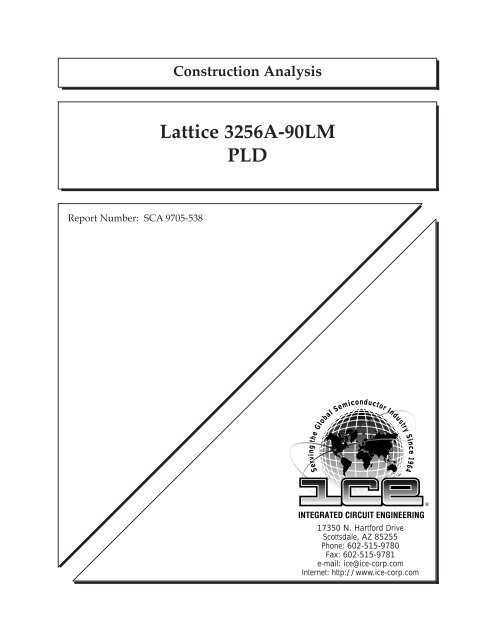
Lattice 3256A-90LM PLD - Smithsonian - The Chip Collection
Lattice 3256A-90LM PLD - Smithsonian - The Chip Collection
Lattice 3256A-90LM PLD - Smithsonian - The Chip Collection

Create successful ePaper yourself
Turn your PDF publications into a flip-book with our unique Google optimized e-Paper software.
Report Number: SCA 9705-538<br />
Construction Analysis<br />
<strong>Lattice</strong> <strong>3256A</strong>-<strong>90LM</strong><br />
<strong>PLD</strong><br />
Serving the Global Semiconductor Industry Since 1964<br />
17350 N. Hartford Drive<br />
Scottsdale, AZ 85255<br />
Phone: 602-515-9780<br />
Fax: 602-515-9781<br />
e-mail: ice@ice-corp.com<br />
Internet: http://www.ice-corp.com<br />
®
TITLE<br />
INDEX TO TEXT<br />
- i -<br />
PAGE<br />
INTRODUCTION 1<br />
MAJOR FINDINGS 1<br />
TECHNOLOGY DESCRIPTION<br />
Die Process 2<br />
ANALYSIS RESULTS I<br />
Die Process and Design 3 - 5<br />
ANALYSIS PROCEDURE 6<br />
TABLES<br />
Overall Quality Evaluation 7<br />
Die Material Analysis (EDX) 8<br />
Horizontal Dimensions 9<br />
Vertical Dimensions 10
INTRODUCTION<br />
This report describes a construction analysis of the <strong>Lattice</strong> <strong>3256A</strong>-<strong>90LM</strong> Programmable<br />
Logic Device (<strong>PLD</strong>). One decapped device was received for the analysis. <strong>The</strong> device was<br />
date coded 9650.<br />
Questionable Items: 1<br />
MAJOR FINDINGS<br />
• Aluminum 1 thinning up to 100 percent 2 (Figure 15). Total metal 1 thinning was<br />
reduced to 90 percent with the addition of the cap and barrier.<br />
Special Features:<br />
• Sub-micron gate lengths (0.5 micron N-channel and 0.6 micron P-channel).<br />
Design Features:<br />
• Slotted and beveled metal 2 bus lines.<br />
1 <strong>The</strong>se items present possible quality or reliability concerns. <strong>The</strong>y should be discussed<br />
with the manufacturer to determine their possible impact on the intended application.<br />
2 Seriousness depends on design margins.<br />
- 1 -
Die Process and Design:<br />
TECHNOLOGY DESCRIPTION<br />
• <strong>The</strong> device was fabricated using a selective oxidation, twin-well CMOS process in a<br />
P-substrate. No epi was used.<br />
• Passivation consisted of a layer of nitride over a layer of silicon-dioxide.<br />
• Metallization employed two levels of metal. Both consisted of aluminum with a<br />
titanium-nitride (TiN) cap and barrier. A thin titanium (Ti) adhesion layer was used<br />
under metal 1. Standard vias and contacts were used (no plugs).<br />
• <strong>The</strong> interlevel dielectric consisted of two layers of glass with a spin-on-glass (SOG)<br />
between the two layers.<br />
• Pre-metal glass consisted of a layer of reflow glass over various densified oxides.<br />
Glass was reflowed prior to contact cuts only.<br />
• A single layer of polycide (tungsten silicide) was used to form one plate of the<br />
capacitors and all gates on the die. Direct poly-to-diffusion (buried) contacts were<br />
not used. Definition was by a dry etch of normal quality.<br />
• Standard implanted N+ and P+ diffusions formed the sources/drains of the CMOS<br />
transistors. An LDD process was used with oxide sidewall spacers left in place.<br />
• Local oxide (LOCOS) isolation. A step was present at the edge of the well which<br />
indicates a twin-well process was used. No problems were noted.<br />
• Two EEPROM cell arrays were used on the device. Both devices are<br />
programmed through an ultra thin (tunnel) oxide window. Metal 2 was used to<br />
form the bit lines and distribute ground on array B. Metal 1 was used for<br />
interconnect and to distribute ground on array A. Poly was used to form the gates<br />
and one plate of the capacitors and gates.<br />
- 2 -
Die Process :<br />
Questionable Items: 1<br />
ANALYSIS RESULTS I<br />
- 3 -<br />
Figures 1 - 36<br />
• Aluminum 1 thinning up to 100 percent 2 (Figure 15). Total metal 1 thinning was<br />
reduced to 90 percent with the addition of the cap and barrier.<br />
Special Features:<br />
• Sub-micron gate lengths (0.5 micron N-channel and 0.6 micron P-channel).<br />
Design features:<br />
• Slotted and beveled metal 2 bus lines.<br />
General items:<br />
• Fabrication process: Devices were fabricated using a selective oxidation, twin-well<br />
CMOS process in a P-substrate. No epi was used.<br />
• Process implementation: Die layout was clean and efficient. Alignment was good at<br />
all levels. No damage of contamination was found.<br />
• Die coat: No die coat was present.<br />
• Overlay passivation: A layer of nitride over a layer of silicon-dioxide. Overlay<br />
integrity test indicated defect-free passivation. Edge seal was good.<br />
1 <strong>The</strong>se items present possible quality or reliability concerns. <strong>The</strong>y should be discussed<br />
with the manufacturer to determine their possible impact on the intended application.<br />
2 Seriousness depends on design margins.
ANALYSIS RESULTS I (continued)<br />
• Metallization: Two levels of metal. Both consisted of aluminum with titanium-<br />
nitride (TiN) caps and barriers. A thin titanium (Ti) adhesion layer was present<br />
beneath metal 1. Standard vias and contacts were used (no plugs).<br />
• Metal patterning: Both metal levels were patterned by a dry etch of normal quality.<br />
• Metal defects: No voiding, notching, or neckdown was noted in the metal of either<br />
layer. Contacts and vias were completely surrounded by metal. No silicon nodules<br />
were noted following removal of either metal layer.<br />
• Metal step coverage: Metal 2 aluminum thinned up to 75 percent at vias. Total metal<br />
2 thinning was reduced to 65 percent with the addition of the cap and barrier. Metal 1<br />
aluminum thinned up to 100 percent at some contacts. Total metal 1 thinning was<br />
reduced to 90 percent with the addition of the cap and barrier.<br />
• Interlevel dielectric: Two layers of silicon-dioxide were present under metal 2<br />
(interlevel dielectric). <strong>The</strong> first layer had been subjected to an etchback process. A<br />
layer of spin-on-glass (SOG) was present between the layers for planarization<br />
purposes.<br />
• Pre-metal glass: A layer of reflow glass over various densified oxides was used<br />
under metal 1. Reflow was performed prior to contact cuts only. No problems were<br />
found.<br />
• Contact defects: Contact and via cuts were defined by a two-step process. No<br />
over-etching of the contacts or vias was noted.<br />
• A single layer of polycide (tungsten silicide) was used to form all gates on the die<br />
and one plate of the capacitors. Direct poly-to-diffusion (buried) contacts were not<br />
used. Definition was by a dry-etch of normal quality.<br />
- 4 -
ANALYSIS RESULTS I (continued)<br />
• Standard implanted N+ and P+ diffusions formed the sources/drains of the CMOS<br />
transistors. An LDD process was used with oxide sidewall spacers left in place. No<br />
problems were found.<br />
• Local oxide (LOCOS) isolation was used with a step present at the well boundary<br />
indicating that a twin-well process was employed.<br />
• Two EEPROM cell arrays were used on the device. Both use the same design (but<br />
different layout) and are programmed through an ultra thin (tunnel) oxide window.<br />
Metal 2 was used to form the bit lines and distribute ground on array B. Metal 1<br />
was used for interconnect and to distribute ground in array A. Poly was used to<br />
form the gates and one plate of the capacitors. Cell size (array A): 9.0 x 9.5<br />
microns. Cell size (array B): 13 x 36 microns<br />
• Redundancy fuses were not present on the die.<br />
- 5 -
PROCEDURE<br />
<strong>The</strong> devices were subjected to the following analysis procedures:<br />
Internal optical inspection<br />
SEM of passivation<br />
Passivation integrity test<br />
Passivation removal<br />
SEM inspection of metal 2<br />
Metal 2 removal and inspect barrier<br />
Delayer to metal 1 and inspect<br />
Metal 1 removal and inspect barrier<br />
Delayer to silicon and inspect poly/die surface<br />
Die sectioning (90° for SEM) *<br />
Die material analysis<br />
Measure horizontal dimensions<br />
Measure vertical dimensions<br />
* Delineation of cross-sections is by silicon etch unless otherwise indicated.<br />
- 6 -
OVERALL QUALITY EVALUATION : Overall Rating: Normal<br />
DETAIL OF EVALUATION<br />
Die surface integrity:<br />
Toolmarks (absence) G<br />
Particles (absence) G<br />
Contamination (absence) G<br />
Process defects G<br />
General workmanship N<br />
Passivation integrity G<br />
Metal definition N<br />
Metal integrity * N<br />
Metal registration N<br />
Contact coverage N<br />
Contact registration N<br />
* Even with the isolated spots where metal 1 thins 100 percent we judge adequate metal<br />
remains around the contact perimeter.<br />
G = Good, P = Poor, N = Normal, NP = Normal/Poor<br />
- 7 -
DIE MATERIAL ANALYSIS<br />
Final passivation: A layer of silicon-nitride over a layer of glass.<br />
Metallization 2: Aluminum (Al) with a titanium-nitride (TiN) cap<br />
and barrier.<br />
Metallization 1: Aluminum (Al) with a titanium-nitride (TiN) cap<br />
and barrier on a thin titanium (Ti) adhesion layer.<br />
Silicide (poly): Tungsten (W).<br />
- 8 -
HORIZONTAL DIMENSIONS<br />
Die size: 7.4 x 9.2 mm (290 x 364 mils)<br />
Die area: 68 mm 2 (105,560 mils 2 )<br />
Min pad size: 0.1 x 0.1 mm (4.0 x 4.0 mils)<br />
Min pad window: 0.09 x 0.09 mm (3.8 x 3.8 mils)<br />
Min pad space: 28 microns<br />
Min metal 2 width: 1.1 micron<br />
Min metal 2 space: 1.1 micron<br />
Min metal 2 pitch: 2.2 microns<br />
Min metal 1 width: 0.8 micron<br />
Min metal 1 space: 0.8 micron<br />
Min metal 1 pitch: 1.6 micron<br />
Min via: 0.85 micron<br />
Min contact: 0.8 micron<br />
Min polycide width: 0.5 micron<br />
Min polycide space: 0.7 micron<br />
Min gate length * - (N-channel): 0.5 micron<br />
- (P-channel): 0.6 micron<br />
Cell pitch (array A): 9.0 x 9.5 microns<br />
Cell size (array A): 85.5 microns 2<br />
Cell pitch (array B): 13 x 35 microns<br />
Cell size (array B): 455 microns 2<br />
* Physical gate length<br />
- 9 -
VERTICAL DIMENSIONS<br />
Die thickness: 0.5 mm (20 mils)<br />
Layers:<br />
Passivation 2: 0.45 micron<br />
Passivation 1: 0.25 micron<br />
Metal 2 - cap: 0.05 micron (approximate)<br />
- aluminum: 0.8 micron<br />
- barrier: 0.12 micron<br />
Interlevel dielectric- glass 2: 0.4 micron<br />
- glass 1: 0.3 micron (average)<br />
Metal 1 - cap: 0.07 micron (approximate)<br />
- aluminum: 0.5 micron<br />
- barrier: 0.12 micron<br />
Pre-metal dielectric: 0.75 micron (average)<br />
Oxide on polycide: 0.15 micron<br />
Polycide - silicide: 0.1 micron<br />
- poly: 0.12 micron<br />
Local oxide: 0.45 micron<br />
N+ S/D: 0.13 micron<br />
P+ S/D: 0.2 micron<br />
N-well: 4.0 microns<br />
P-well: 4.0 microns<br />
- 10 -
INDEX TO FIGURES<br />
DIE LAYOUT AND IDENTIFICATION Figures 1 - 3<br />
PHYSICAL DIE STRUCTURES Figures 4 - 39<br />
COLOR DRAWING OF DIE STRUCTURE Figure 21<br />
EEPROM CELL (ARRAY A) Figures 22 - 28<br />
EEPROM CELL (ARRAY B) Figures 29 - 35<br />
INPUT PROTECTION CIRCUIT Figure 36<br />
GENERAL CIRCUIT LAYOUT Figure 36<br />
- ii -
<strong>Lattice</strong> <strong>3256A</strong>-<strong>90LM</strong><br />
Figure 1. Whole die photograph of the <strong>Lattice</strong> <strong>3256A</strong>-<strong>90LM</strong>. Mag. 25x.<br />
Integrated Circuit Engineering Corporation
<strong>Lattice</strong> <strong>3256A</strong>-<strong>90LM</strong><br />
Figure 2. Markings from the die surface. Mag. 320x.<br />
Integrated Circuit Engineering Corporation
Figure 3. Optical views of the die corners on the <strong>Lattice</strong> <strong>3256A</strong>-<strong>90LM</strong>. Mag. 160x.<br />
<strong>Lattice</strong> <strong>3256A</strong>-<strong>90LM</strong><br />
Integrated Circuit Engineering Corporation
<strong>Lattice</strong> <strong>3256A</strong>-<strong>90LM</strong><br />
Mag. 170x<br />
Mag. 600x<br />
Figure 4. Perspective SEM views of dicing and edge seal. 60°.<br />
Integrated Circuit Engineering Corporation
<strong>Lattice</strong> <strong>3256A</strong>-<strong>90LM</strong><br />
DIE EDGE<br />
METAL 1<br />
METAL 2<br />
METAL 1<br />
METAL 2<br />
Figure 5. SEM section views of the edge seal.<br />
Integrated Circuit Engineering Corporation<br />
Mag. 1400x<br />
Mag. 3200x<br />
Mag. 6500x
<strong>Lattice</strong> <strong>3256A</strong>-<strong>90LM</strong><br />
POLY<br />
METAL 2<br />
INTERLEVEL DIELECTRIC<br />
N+ S/D<br />
METAL 2<br />
N+ S/D<br />
METAL 1<br />
Figure 6. SEM section views of general device structure. Mag. 10,000x.<br />
Integrated Circuit Engineering Corporation<br />
METAL 1
<strong>Lattice</strong> <strong>3256A</strong>-<strong>90LM</strong><br />
Mag. 5200x<br />
Mag. 10,000x<br />
Figure 7. Perspective SEM views of overlay passivation coverage. 60°.<br />
Integrated Circuit Engineering Corporation
<strong>Lattice</strong> <strong>3256A</strong>-<strong>90LM</strong><br />
Mag. 13,000x<br />
PASSIVATION 2<br />
PASSIVATION 1<br />
ALUMINUM 2<br />
PASSIVATION<br />
METAL 2<br />
METAL 1<br />
INTERLEVEL DIELECTRIC<br />
Mag. 26,000x<br />
INTERLEVEL DIELECTRIC<br />
TiN CAP<br />
TiN BARRIER<br />
Figure 8. SEM section views of metal 2 line profiles.<br />
Integrated Circuit Engineering Corporation
<strong>Lattice</strong> <strong>3256A</strong>-<strong>90LM</strong><br />
VIA<br />
METAL 2<br />
Mag. 2000x<br />
METAL 2<br />
Mag. 4000x<br />
Figure 9. Topological SEM views of metal 2 patterning.<br />
Integrated Circuit Engineering Corporation
<strong>Lattice</strong> <strong>3256A</strong>-<strong>90LM</strong><br />
PASSIVATION<br />
METAL 2<br />
METAL 1<br />
METAL 2<br />
METAL 2<br />
INTERLEVEL DIELECTRIC<br />
Figure 10. SEM views of metal 2 coverage and via.<br />
Integrated Circuit Engineering Corporation<br />
Mag. 6500x<br />
Mag. 13,000x<br />
Mag. 26,000x
<strong>Lattice</strong> <strong>3256A</strong>-<strong>90LM</strong><br />
PRE-METAL DIELECTRIC<br />
Mag. 40,000x<br />
ALUMINUM 1<br />
Mag. 52,000x<br />
Figure 11. SEM section views of metal 1 line profiles.<br />
Integrated Circuit Engineering Corporation<br />
INTERLEVEL<br />
DIELECTRIC<br />
ALUMINUM 1<br />
TiN CAP<br />
SOG<br />
TiN BARRIER
<strong>Lattice</strong> <strong>3256A</strong>-<strong>90LM</strong><br />
Mag. 3200x<br />
METAL 1<br />
Mag. 6500x<br />
METAL 1<br />
CONTACT<br />
Figure 12. Topological SEM views of metal 1 patterning. 0°.<br />
Integrated Circuit Engineering Corporation
<strong>Lattice</strong> <strong>3256A</strong>-<strong>90LM</strong><br />
METAL 1<br />
Mag. 6500x<br />
CONTACT<br />
Mag. 20,000x<br />
METAL 1<br />
Figure 13. Perspective SEM views of metal 1 coverage. 60°.<br />
Integrated Circuit Engineering Corporation
<strong>Lattice</strong> <strong>3256A</strong>-<strong>90LM</strong><br />
SOG<br />
60°<br />
METAL 1<br />
glass etch<br />
Integrated Circuit Engineering Corporation<br />
TiN<br />
BARRIER<br />
PRE-METAL<br />
DIELECTRIC<br />
POLY<br />
Figure 14. SEM views of barrier coverage and a metal contact. Mag. 26,000x.
<strong>Lattice</strong> <strong>3256A</strong>-<strong>90LM</strong><br />
SOG<br />
100%<br />
THINNING<br />
METAL 1<br />
P+ S/D<br />
METAL 1<br />
N+ S/D<br />
POLY<br />
INTERLEVEL<br />
DIELECTRIC<br />
POLY<br />
POLY<br />
Integrated Circuit Engineering Corporation<br />
PRE-METAL<br />
DIELECTRIC<br />
metal 1-to-P+<br />
metal 1-to-N+<br />
Figure 15. SEM section views of typical metal 1 contacts. Mag. 26,000x.<br />
SOG<br />
P+ S/D<br />
PRE-METAL<br />
DIELECTRIC<br />
N+ S/D<br />
METAL 1<br />
PRE-METAL<br />
DIELECTRIC<br />
metal 1-to-poly
<strong>Lattice</strong> <strong>3256A</strong>-<strong>90LM</strong><br />
POLY<br />
Mag. 3200x<br />
POLY<br />
Mag. 6500x<br />
Figure 16. Topological SEM views of poly patterning. 0°.<br />
N+<br />
P+<br />
Integrated Circuit Engineering Corporation
<strong>Lattice</strong> <strong>3256A</strong>-<strong>90LM</strong><br />
POLY<br />
DIFFUSION<br />
POLY<br />
DIFFUSION<br />
LOCAL<br />
OXIDE<br />
LOCAL<br />
OXIDE<br />
POLY<br />
Figure 17. Perspective SEM views of poly coverage. 60°.<br />
Integrated Circuit Engineering Corporation<br />
Mag. 6500x<br />
Mag. 40,000x<br />
Mag. 40,000x
<strong>Lattice</strong> <strong>3256A</strong>-<strong>90LM</strong><br />
P+ S/D<br />
N+ S/D<br />
PRE-METAL<br />
DIELECTRIC<br />
GATE<br />
OXIDE<br />
PRE-METAL<br />
DIELECTRIC<br />
POLY<br />
POLY<br />
PRE-METAL<br />
DIELECTRIC<br />
GATE<br />
OXIDE<br />
P+ S/D<br />
SIDEWALL<br />
SPACER<br />
N+ S/D<br />
Figure 18. SEM section views of typical transistors. Mag. 52,000x.<br />
Integrated Circuit Engineering Corporation<br />
METAL 1<br />
glass etch<br />
P-channel<br />
N-channel
<strong>Lattice</strong> <strong>3256A</strong>-<strong>90LM</strong><br />
LOCAL<br />
OXIDE<br />
Figure 19. SEM section view of a local oxide birdsbeak. Mag. 52,000x.<br />
LOCAL<br />
OXIDE<br />
STEP<br />
PRE-METAL<br />
DIELECTRIC<br />
P-WELL<br />
P-SUBSTRATE<br />
BIRDSBEAK<br />
POLY<br />
N-WELL<br />
Figure 20. Section views of the well structure.<br />
Integrated Circuit Engineering Corporation<br />
Mag. 26,000x<br />
Mag. 800x
,,,,,,,,,,,,,,,,,,,,,<br />
INTERLEVEL ,,,,,,,<br />
DIELECTRIC<br />
,,,,,,,,,,,,,,,,,,,,,<br />
,,,,,,,<br />
SOG<br />
,,,,,,,,,,,,,,,,,,,,,<br />
,,,,,,,<br />
N+ S/D<br />
,,,,,,,,,,<br />
,,,,,,,,,,<br />
P-WELL<br />
POLY<br />
LOCAL<br />
OXIDE<br />
METAL 1<br />
METAL 2<br />
PRE-METAL DIELECTRIC<br />
P+ S/D<br />
Orange = Nitride, Blue = Metal, Yellow = Oxide, Green = Poly,<br />
Red = Diffusion, and Gray = Substrate<br />
Figure 21. Color cross section drawing illustrating device structure.<br />
PASSIVATION 2<br />
PASSIVATION 1<br />
,,,,,,,,,,,,,<br />
,,,,,,,,,,,,,<br />
,,,,,,,,,,,,,<br />
,,,,,,,,,,,,,<br />
N-WELL<br />
<strong>Lattice</strong> <strong>3256A</strong>-<strong>90LM</strong><br />
Integrated Circuit Engineering Corporation
<strong>Lattice</strong> <strong>3256A</strong>-<strong>90LM</strong><br />
Integrated Circuit Engineering Corporation<br />
metal 2<br />
metal 1<br />
poly<br />
Figure 22. Perspective SEM views of the EEPROM cell array. Array A, Mag. 3200x,<br />
60°.
<strong>Lattice</strong> <strong>3256A</strong>-<strong>90LM</strong><br />
Mag. 6500x<br />
Mag. 26,000x<br />
TUNNEL OXIDE<br />
DEVICE<br />
Figure 23. Detailed SEM views of the EEPROM cell array. Array A, 60°.<br />
Integrated Circuit Engineering Corporation
<strong>Lattice</strong> <strong>3256A</strong>-<strong>90LM</strong><br />
Integrated Circuit Engineering Corporation<br />
metal 2<br />
metal 1<br />
poly<br />
Figure 24. SEM views of the EEPROM cell array. Array A, Mag. 1600x, 0°.
<strong>Lattice</strong> <strong>3256A</strong>-<strong>90LM</strong><br />
BIT<br />
BIT<br />
B<br />
metal 2<br />
metal 1<br />
Integrated Circuit Engineering Corporation<br />
Figure 25. Additional SEM views of the EEPROM cell array. Array A, Mag. 3200x,<br />
A<br />
GND
<strong>Lattice</strong> <strong>3256A</strong>-<strong>90LM</strong><br />
C<br />
BIT<br />
C<br />
2<br />
1<br />
poly<br />
WORD<br />
2<br />
1<br />
B<br />
Integrated Circuit Engineering Corporation<br />
Figure 26. SEM view and schematic of the EEPROM cell. Array A, Mag. 3200x, 0°.
<strong>Lattice</strong> <strong>3256A</strong>-<strong>90LM</strong><br />
TUNNEL<br />
OXIDE<br />
WINDOW<br />
Figure 27. Topological SEM view of the tunnel oxide window. Array A,<br />
Mag. 13,000x, 0°.<br />
Integrated Circuit Engineering Corporation
<strong>Lattice</strong> <strong>3256A</strong>-<strong>90LM</strong><br />
N+ S/D<br />
SELECT<br />
GATE<br />
N+ S/D<br />
GATE<br />
OXIDE<br />
TUNNEL<br />
OXIDE<br />
DEVICE<br />
POLY SELECT GATE<br />
POLY<br />
TUNNEL<br />
OXIDE<br />
METAL 1<br />
POLY<br />
GATE<br />
PRE-METAL<br />
DIELECTRIC<br />
N+ S/D<br />
Figure 28. SEM section views of an EEPROM cell. Array A.<br />
Integrated Circuit Engineering Corporation<br />
N+ S/D<br />
Mag. 13,000x<br />
Mag. 40,000x<br />
Mag. 52,000x
<strong>Lattice</strong> <strong>3256A</strong>-<strong>90LM</strong><br />
Integrated Circuit Engineering Corporation<br />
metal 2<br />
metal 1<br />
poly<br />
Figure 29. Perspective SEM views of the additional EEPROM cell array. Array B,<br />
Mag. 1600x, 60°.
<strong>Lattice</strong> <strong>3256A</strong>-<strong>90LM</strong><br />
Integrated Circuit Engineering Corporation<br />
metal 2<br />
metal 1<br />
poly<br />
Figure 30. SEM views of additional EEPROM cells. Array B, Mag. 1600x.
<strong>Lattice</strong> <strong>3256A</strong>-<strong>90LM</strong><br />
BIT 0<br />
GND<br />
metal 2<br />
metal 1<br />
Integrated Circuit Engineering Corporation<br />
Figure 31. Detailed SEM views of additional EEPROM cell. Array B, Mag. 3200x. 0°.<br />
A<br />
B<br />
BIT 1
<strong>Lattice</strong> <strong>3256A</strong>-<strong>90LM</strong><br />
BIT 0<br />
WORD<br />
BIT 1<br />
1<br />
C1<br />
C1<br />
WORD<br />
2<br />
poly<br />
Integrated Circuit Engineering Corporation<br />
Figure 32. Detailed SEM view and schematic of additional EEPROM cell. Array B,<br />
Mag. 3200x, 0°.<br />
1<br />
2<br />
A<br />
3<br />
B<br />
3
<strong>Lattice</strong> <strong>3256A</strong>-<strong>90LM</strong><br />
N+ S/D<br />
SELECT<br />
GATE<br />
METAL 1<br />
TUNNEL<br />
OXIDE<br />
DEVICE<br />
Mag. 10,000x<br />
POLY<br />
METAL 2<br />
TUNNEL<br />
OXIDE<br />
Mag. 40,000x<br />
POLY<br />
GATE<br />
Figure 33. SEM section views of additional EEPROM cell. Array B.<br />
Integrated Circuit Engineering Corporation<br />
N+ S/D
<strong>Lattice</strong> <strong>3256A</strong>-<strong>90LM</strong><br />
N+<br />
N+<br />
TUNNEL<br />
OXIDE<br />
POLY<br />
TUNNEL<br />
OXIDE<br />
METAL 1<br />
TUNNEL<br />
OXIDE<br />
DEVICE<br />
PRE-METAL<br />
DIELECTRIC<br />
POLY<br />
CAPACITOR<br />
Figure 34. SEM section views of additional EEPROM cell. Array B.<br />
Integrated Circuit Engineering Corporation<br />
Mag. 5000x<br />
Mag. 37,000x<br />
Mag. 52,000x
<strong>Lattice</strong> <strong>3256A</strong>-<strong>90LM</strong><br />
POLY<br />
CAPACITOR<br />
CAPACITORS<br />
Mag. 8000x<br />
Mag. 20,000x<br />
METAL 1<br />
Integrated Circuit Engineering Corporation<br />
Figure 35. SEM section views of additional EEPROM cell through the capacitor region.<br />
Array B.
<strong>Lattice</strong> <strong>3256A</strong>-<strong>90LM</strong><br />
Mag. 320x<br />
Mag. 800x<br />
Figure 36. Optical views of an I/O structure and general circuitry.<br />
Integrated Circuit Engineering Corporation