Programmable Logic and Application Specific Integrated Circuits
Programmable Logic and Application Specific Integrated Circuits
Programmable Logic and Application Specific Integrated Circuits

You also want an ePaper? Increase the reach of your titles
YUMPU automatically turns print PDFs into web optimized ePapers that Google loves.
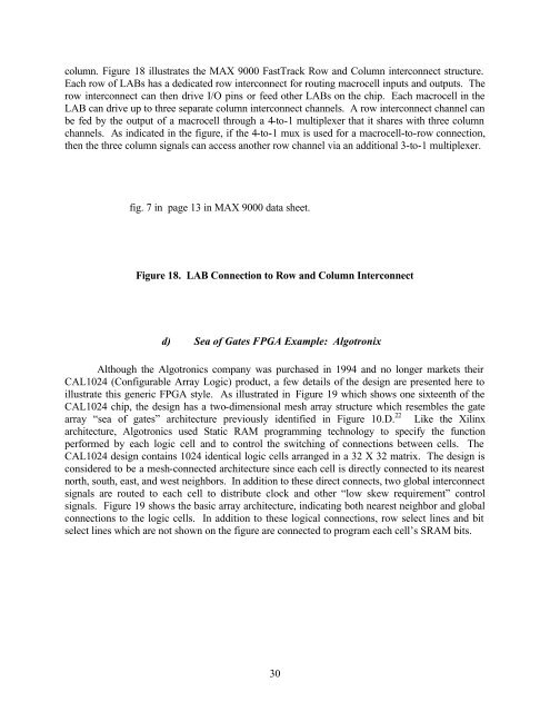
column. Figure 18 illustrates the MAX 9000 FastTrack Row <strong>and</strong> Column interconnect structure.<br />
Each row of LABs has a dedicated row interconnect for routing macrocell inputs <strong>and</strong> outputs. The<br />
row interconnect can then drive I/O pins or feed other LABs on the chip. Each macrocell in the<br />
LAB can drive up to three separate column interconnect channels. A row interconnect channel can<br />
be fed by the output of a macrocell through a 4-to-1 multiplexer that it shares with three column<br />
channels. As indicated in the figure, if the 4-to-1 mux is used for a macrocell-to-row connection,<br />
then the three column signals can access another row channel via an additional 3-to-1 multiplexer.<br />
fig. 7 in page 13 in MAX 9000 data sheet.<br />
Figure 18. LAB Connection to Row <strong>and</strong> Column Interconnect<br />
d) Sea of Gates FPGA Example: Algotronix<br />
Although the Algotronics company was purchased in 1994 <strong>and</strong> no longer markets their<br />
CAL1024 (Configurable Array <strong>Logic</strong>) product, a few details of the design are presented here to<br />
illustrate this generic FPGA style. As illustrated in Figure 19 which shows one sixteenth of the<br />
CAL1024 chip, the design has a two-dimensional mesh array structure which resembles the gate<br />
array “sea of gates” architecture previously identified in Figure 10.D. 22 Like the Xilinx<br />
architecture, Algotronics used Static RAM programming technology to specify the function<br />
performed by each logic cell <strong>and</strong> to control the switching of connections between cells. The<br />
CAL1024 design contains 1024 identical logic cells arranged in a 32 X 32 matrix. The design is<br />
considered to be a mesh-connected architecture since each cell is directly connected to its nearest<br />
north, south, east, <strong>and</strong> west neighbors. In addition to these direct connects, two global interconnect<br />
signals are routed to each cell to distribute clock <strong>and</strong> other “low skew requirement” control<br />
signals. Figure 19 shows the basic array architecture, indicating both nearest neighbor <strong>and</strong> global<br />
connections to the logic cells. In addition to these logical connections, row select lines <strong>and</strong> bit<br />
select lines which are not shown on the figure are connected to program each cell’s SRAM bits.<br />
30