Analog Circuit Design Laboratory Report - MyWeb at WIT ...
Analog Circuit Design Laboratory Report - MyWeb at WIT ...
Analog Circuit Design Laboratory Report - MyWeb at WIT ...

You also want an ePaper? Increase the reach of your titles
YUMPU automatically turns print PDFs into web optimized ePapers that Google loves.
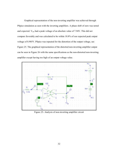
Graphical represent<strong>at</strong>ion of the non-inverting amplifier was achieved through<br />
PSpice simul<strong>at</strong>ion as seen with the inverting amplifiers. A phase shift of zero was noted<br />
and expected. Vout had a peak voltage of an absolute value of 7.94V. This did not<br />
compare favorably and was calcul<strong>at</strong>ed to be within 10.8% of our expected peak output<br />
voltage of 8.905V. PSpice was repe<strong>at</strong>ed for the distortion of the output voltage, see<br />
Figure 25. The graphical represent<strong>at</strong>ion of the distorted non-inverting amplifier output<br />
can be seen in Figure 26 with the same specific<strong>at</strong>ions as the non-distorted non-inverting<br />
amplifier except having too high of an output voltage value.<br />
Figure 25- Analysis of non-inverting amplifier circuit<br />
32