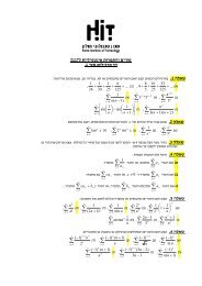
Experiment 5 â Coupler Design.
Experiment 5 â Coupler Design.
Experiment 5 â Coupler Design.

Create successful ePaper yourself
Turn your PDF publications into a flip-book with our unique Google optimized e-Paper software.
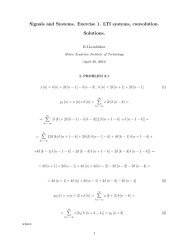
SSub<br />
SSUB<br />
SSub1<br />
Er=4.7<br />
Mur=1<br />
B=0.32 cm<br />
T=0.035 mm<br />
Cond=1.0E+50<br />
TanD=0.02<br />
S-PARAMETERS<br />
S_Param<br />
SP1<br />
Start=500 MHz<br />
Stop=1500 MHz<br />
Step=1.0 MHz<br />
Term<br />
Term1<br />
Num=1<br />
Z=50 Ohm<br />
Term<br />
Term4<br />
Num=4<br />
Z=50 Ohm<br />
SCLIN<br />
CLin1<br />
Subst="SSub1"<br />
W=cm<br />
S=cm<br />
L=cm<br />
Term<br />
Term3<br />
Num=3<br />
Z=50 Ohm<br />
Term<br />
Term2<br />
Num=2<br />
Z=50 Ohm<br />
Figure 1 - Single section edge coupled lines coupler.<br />
2. Draw the following graphs:<br />
• Coupling (dB).<br />
• Directivity (dB).<br />
• Insertion Loss (dB).<br />
• VSWR primary and secondary line.<br />
• Frequency sensitivity (of the primary line), frequency range 800 MHz−<br />
1200 MHz. Save the data.<br />
4.2.2 CST Simulation of a Microstrip <strong>Coupler</strong><br />
1. Choose the "<strong>Coupler</strong> (Planar, Microstrip, cpw)" template. When this<br />
template is used, the background material is defined as vacuum, the<br />
units are changed to mm, GHz and nsec, and the boundary conditions<br />
are set to "electric". Furthermore, the mesh settings are changed to<br />
account for the planar structure.<br />
2. Define the parameters, as shown in Table 1.<br />
11