

Contacts for Flip Chip Wafer Level Probing - Semiconductor Wafer ...
Contacts for Flip Chip Wafer Level Probing - Semiconductor Wafer ...
Contacts for Flip Chip Wafer Level Probing - Semiconductor Wafer ...
SHOW LESS

Create successful ePaper yourself
Turn your PDF publications into a flip-book with our unique Google optimized e-Paper software.
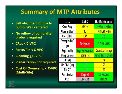
Summary of MTP Attributes<br />
• Self alignment of tips to<br />
bump. Well centered<br />
• No reflow of bump after<br />
probe is required<br />
• CRes < C‐VPC<br />
• Force/Pin < C‐VPC<br />
• Cleaning < C‐VPC<br />
• Planarization not required<br />
• Cost Of Ownership < C‐VPC<br />
(Multi‐Site)


