The Generic Foundry Model in Europe - JePPIX
The Generic Foundry Model in Europe - JePPIX
The Generic Foundry Model in Europe - JePPIX

Create successful ePaper yourself
Turn your PDF publications into a flip-book with our unique Google optimized e-Paper software.
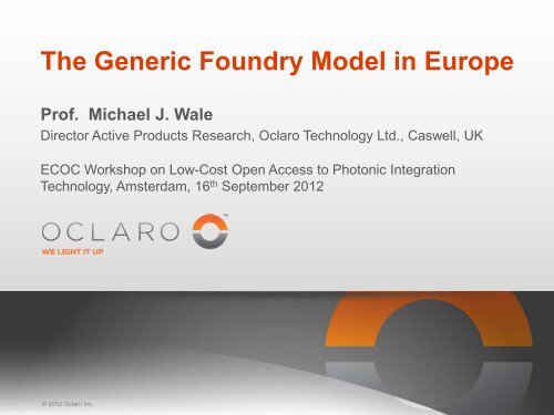
<strong>The</strong> <strong>Generic</strong> <strong>Foundry</strong> <strong>Model</strong> <strong>in</strong> <strong>Europe</strong><br />
Prof. Michael J. Wale<br />
Director Active Products Research, Oclaro Technology Ltd., Caswell, UK<br />
ECOC Workshop on Low-Cost Open Access to Photonic Integration<br />
Technology, Amsterdam, 16 th September 2012<br />
1 © 2012 Oclaro Inc.
Agenda<br />
• Motivation<br />
• <strong>Generic</strong> Platform Concepts and Methodology<br />
• Current platform developments <strong>in</strong> <strong>Europe</strong><br />
– InP (<strong>JePPIX</strong>)<br />
– Silicon Photonics (ePIXfab)<br />
– Dielectric planar lightwave circuits (TriPleX)<br />
• Conclusions<br />
2 © 2012 Oclaro Inc.<br />
2
Photonic Integration: Motivation<br />
• Greatly reduced component cost<br />
• Monolithic <strong>in</strong>terconnection of device elements<br />
• Simpler packag<strong>in</strong>g and assembly, standard processes<br />
• High reliability<br />
• Less <strong>in</strong>terfaces<br />
• High functionality<br />
• Many more functional elements per chip, higher creativity <strong>in</strong> design<br />
• High phase stability, excellent device match<strong>in</strong>g<br />
• Permits <strong>in</strong>terferometric structures<br />
• Robust<br />
• S<strong>in</strong>gle chip designs with m<strong>in</strong>imal optical <strong>in</strong>terfaces are ideal for demand<strong>in</strong>g<br />
environments<br />
• Better power efficiency<br />
• M<strong>in</strong>imize optical power loss at <strong>in</strong>terfaces between device elements<br />
PIC Technologies have high value<br />
3 © 2012 Oclaro Inc.
Photonic Integration <strong>in</strong> Oclaro<br />
• Photonic <strong>in</strong>tegration is central to Oclaro’s<br />
bus<strong>in</strong>ess<br />
• Highly flexible active-passive <strong>in</strong>tegration<br />
scheme based on selective area epitaxy<br />
on InP<br />
– Butt-jo<strong>in</strong>s between active and passive<br />
sections<br />
• Multiple stages of epitaxy us<strong>in</strong>g MOVPE<br />
– 3-6 growth stages<br />
– High yields<br />
• Fabrication at Caswell, UK<br />
– Major <strong>in</strong>vestment <strong>in</strong> equipment, facilities<br />
and R&D<br />
– 3” process<strong>in</strong>g, stepper and e-beam<br />
lithography, extensive automation<br />
• Builds on work done over >20 years with<br />
significant support of EC<br />
Example: Monolithic<br />
Laser + Modulator chip<br />
for Tunable XFP module<br />
• ~1000 chips per wafer<br />
• Batch processed<br />
• 3” InP wafers<br />
• On-wafer tested<br />
• Scalable<br />
4 © 2012 Oclaro Inc.
Economics of Integration<br />
• Range of applications for <strong>in</strong>tegrated photonics is extremely wide<br />
• Many applications can only be addressed us<strong>in</strong>g photonic <strong>in</strong>tegration<br />
– Cost, performance, stability<br />
• PIC real-estate is potentially cheap<br />
– Even with complex functionality, ~ 1000 die sites on 3” InP wafer<br />
– Automated fabs with high level of process control provide good yields<br />
• Cost of entry is very high: photonic <strong>in</strong>tegration is available only to a very<br />
few companies today (fab, design costs, …)<br />
• Need to <strong>in</strong>crease market size and reduce the cost of entry for new<br />
applications for the <strong>in</strong>dustry to flourish<br />
– PICs can be a major enabler for new markets<br />
– Increased return on <strong>in</strong>vestment for next-generation wafer fabs<br />
• An alternative approach:<br />
– “<strong>Generic</strong>” foundry approach for arbitrary applications on a common,<br />
qualified process base<br />
– Design systems that allow user-specified designs to be right first time<br />
– Very like ASICs <strong>in</strong> silicon microelectronics<br />
5 © 2012 Oclaro Inc.
<strong>The</strong> ePIXnet proposition<br />
6 © 2012 Oclaro Inc.
<strong>The</strong> ePIXnet vision<br />
• Convergence of technologies<br />
• develop a limited number of generic wafer-scale <strong>in</strong>tegration<br />
technologies that can support a broad range of applications<br />
• Convergence of design approaches<br />
• decouple design (IP) from technology (IP)<br />
• set up libraries<br />
• standardize <strong>in</strong>terfaces of design tools<br />
• Tra<strong>in</strong><strong>in</strong>g<br />
• organize tra<strong>in</strong><strong>in</strong>g and design support for researchers and SMEs, <strong>in</strong><br />
particular fabless companies<br />
• F<strong>in</strong>d the ePIXnet vision paper at www.epixnet.org<br />
7 © 2012 Oclaro Inc.
<strong>Generic</strong> Integration Philosophy<br />
Electronic <strong>in</strong>tegration<br />
3 basic build<strong>in</strong>g blocks<br />
Photonic <strong>in</strong>tegration<br />
4 basic build<strong>in</strong>g blocks<br />
PWD<br />
Waveguide<br />
PHM<br />
ϕ<br />
Phase<br />
SOA<br />
Α<br />
Amplitude<br />
P<br />
Polarization<br />
8 © 2012 Oclaro Inc.
Build<strong>in</strong>g with basic functional blocks<br />
Passive Phase Amplitude<br />
Polarisation<br />
waveguide<br />
phase modulator<br />
optical amplifier<br />
polarisation converter<br />
curve<br />
amplitude modulator<br />
λ converter, ultrafast switch<br />
pol. splitter / comb<strong>in</strong>er<br />
MMI-coupler<br />
2x2 switch<br />
picosecond pulse laser<br />
pol. <strong>in</strong>dep. 2x2 switch<br />
AWG-demux<br />
WDM OXC<br />
multiwavelength laser<br />
pol. <strong>in</strong>dep. diff. delay l<strong>in</strong>e<br />
9 © 2012 Oclaro Inc.
<strong>Generic</strong> <strong>Foundry</strong> Platform <strong>Model</strong><br />
• <strong>Generic</strong> design and manufactur<strong>in</strong>g platforms are based on standard process flows<br />
and structures<br />
• <strong>The</strong> foundry can<br />
accord<strong>in</strong>gly turn wafers <strong>in</strong><br />
high volume on stable<br />
processes, support<strong>in</strong>g<br />
many different designs<br />
• We can establish a<br />
separation of function<br />
between specification,<br />
design and fab<br />
• We can develop dedicated<br />
software tools and a<br />
component library for<br />
rapid and accurate chip<br />
design<br />
• This model is used to great effect <strong>in</strong> microelectronics, but until now has never been<br />
applied <strong>in</strong> photonics<br />
10 © 2012 Oclaro Inc.
<strong>Generic</strong> PIC <strong>Foundry</strong> - Potential Impact<br />
• Photonic ICs come with<strong>in</strong> reach for a much wider range<br />
of users and applications<br />
• Design capability and design productivity greatly<br />
<strong>in</strong>creased<br />
– Move from photonic device development to photonic<br />
circuit design<br />
– New skills, new <strong>in</strong>dustries <strong>in</strong> PIC design will emerge<br />
• High manufactur<strong>in</strong>g volumes on standard processes<br />
• Designs that pass design rule checks are automatically<br />
qualified for reliability, so elim<strong>in</strong>at<strong>in</strong>g an expensive and<br />
time-consum<strong>in</strong>g part of product development<br />
• PIC development and manufactur<strong>in</strong>g cost is no longer<br />
the bottle neck<br />
11 © 2012 Oclaro Inc.
Chip cost trends <strong>in</strong> different fab models<br />
Entry costs<br />
Cleanroom<br />
Process<br />
Design<br />
1B<br />
1M<br />
Chip cost / mm 2<br />
Vertical Custom <strong>Generic</strong><br />
1995 2005 2015<br />
1k<br />
Values are <strong>in</strong>dicative only<br />
1<br />
1 10 100 1k 10k 100k 1M 10M<br />
1 10 100 1,000 10,000 100,000 1,000,000 10,000,000<br />
Chip volume (mm 2 )<br />
12 © 2012 Oclaro Inc.
<strong>Generic</strong> technology landscape <strong>in</strong> <strong>Europe</strong><br />
TripleX<br />
2005<br />
ePIXfab<br />
ePIX net<br />
2007<br />
<strong>JePPIX</strong><br />
STW<br />
GTIP<br />
EuroPIC<br />
Network<br />
Platform<br />
IoP<br />
PD<br />
Memphis<br />
Paradigm<br />
EU Project<br />
NL Project<br />
13 © 2012 Oclaro Inc.
<strong>JePPIX</strong>: <strong>The</strong> <strong>Europe</strong>an InP PIC Platform<br />
• <strong>JePPIX</strong> is the Jo<strong>in</strong>t <strong>Europe</strong>an<br />
Platform for Photonic Integration of<br />
InP-based Components and Circuits<br />
• Provides a framework for research,<br />
development, dissem<strong>in</strong>ation and<br />
exploitation of generic InP PIC<br />
technology<br />
• Supports design-rule, library-based<br />
generic platforms for InP PICs<br />
• Current and recent projects:<br />
EuroPIC, PARADIGM (FP7),<br />
MEMPHIS (NL)<br />
• Contact: Coord<strong>in</strong>ator@<strong>JePPIX</strong>.eu<br />
• Download the <strong>JePPIX</strong> roadmap at<br />
www.<strong>JePPIX</strong>.eu<br />
14 © 2012 Oclaro Inc.
InP Application-Specific PICs from the EuroPIC project<br />
WDM receiver for FTTH Filtered Feedback MW laser hybrid TDM-WDM transmitters FBG-readout<br />
(user Genexis, fab HHI) (user ASTRON, fab Oclaro) (user Genexis, fab Oclaro) (user Fibresens<strong>in</strong>g, fab HHI)<br />
Fast optical switch matrix Pulse serialiser Pulse regenerator Pulse shaper<br />
(user UCamb, fab Oclaro) for KM3NeT neutr<strong>in</strong>o detector (user U Pisa, fab COBRA) for bio-imag<strong>in</strong>g<br />
(user NIKHEF, fab Oclaro)<br />
(user UTwente, fab Oclaro)<br />
non-telecom<br />
15 © 2012 Oclaro Inc.
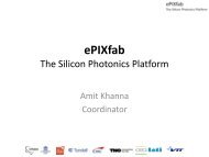
Silicon Photonics: ePIXfab<br />
Objective: Establish access to silicon photonics technology<br />
for small scale users and support emergence of a fab-less<br />
ecosystem<br />
• IC technology (Multi Project Wafers)<br />
• Packag<strong>in</strong>g & Integration<br />
• Tra<strong>in</strong><strong>in</strong>g & Support<br />
ePIXfab is a collaboration between research <strong>in</strong>stitutes, coord<strong>in</strong>ated by IMEC<br />
2006 2011<br />
Supported by the EU (FP6, FP7)<br />
16 © 2012 Oclaro Inc.
ePIXfab achievements<br />
Industry<br />
Research Institute<br />
University<br />
17 © 2012 Oclaro Inc.
Elements realized <strong>in</strong> the ePIXfab process at IMEC<br />
High conf<strong>in</strong>ement<br />
waveguide, 450nm width x<br />
220nm height<br />
R<strong>in</strong>g resonator<br />
Waveguide<br />
cross<strong>in</strong>g<br />
Spiral waveguide<br />
AWG multiplexer with channel spac<strong>in</strong>g 200GHz, size 250µmx200µm<br />
18 © 2012 Oclaro Inc.
TriPleX Platform<br />
19 © 2012 Oclaro Inc.
TriPleX Platform - MPW<br />
http://www.lionixbv.nl/<br />
20 © 2012 Oclaro Inc.
A message from a pioneer <strong>in</strong> silicon VLSI<br />
“When new design methods are<br />
<strong>in</strong>troduced <strong>in</strong> any technology, especially <strong>in</strong><br />
a new technology, a large-scale<br />
exploratory application of the methods by<br />
many designers is necessary <strong>in</strong> order to<br />
test and validate the methods …<br />
A lot of usage is necessary to enable<br />
sufficient viewpo<strong>in</strong>t shifts and social<br />
organization shifts to occur to effect the<br />
cultural <strong>in</strong>tegration of the methods.”<br />
Lynn Conway, coauthor ‘Introduction to<br />
VLSI systems’ (1979), from PARC report<br />
‘<strong>The</strong> MPC Adventures” (1981)<br />
<strong>Europe</strong>an platform projects are start<strong>in</strong>g this process for PICs<br />
21 © 2012 Oclaro Inc.
Conclusions<br />
• Photonic <strong>in</strong>tegration is a breakthrough technology<br />
• Need to <strong>in</strong>crease market size and reduce the cost of entry for<br />
new applications for the <strong>in</strong>dustry to flourish<br />
– PICs can be a major enabler for new markets<br />
– Increased return on <strong>in</strong>vestment for next-generation wafer fabs<br />
• <strong>Generic</strong> foundry approach looks promis<strong>in</strong>g<br />
– Establish generic methodology, standard platforms, design tools, packag<strong>in</strong>g<br />
approaches ...<br />
– Potential for dramatic reduction of entry costs for new applications<br />
– <strong>The</strong>re are uncerta<strong>in</strong>ties but also major creative opportunities – just as <strong>in</strong><br />
VLSI<br />
• <strong>The</strong> <strong>Europe</strong>an Photonics Community is tak<strong>in</strong>g important steps<br />
towards the validation of the generic foundry model <strong>in</strong> PIC R&D<br />
and Manufactur<strong>in</strong>g<br />
• <strong>The</strong> dom<strong>in</strong>ant model <strong>in</strong> 5-10 years?<br />
22 © 2012 Oclaro Inc.
Acknowledgments<br />
• <strong>The</strong> author would to thank the many people who have contributed<br />
to the development of <strong>Generic</strong> PIC platforms <strong>in</strong> <strong>Europe</strong><br />
• This work has been supported <strong>in</strong> part by the <strong>Europe</strong>an<br />
Commission through the ePIXnet, EuroPIC, PARADIGM,<br />
PhotonFab, ESSenTIAL and HELIOS projects and by the Dutch<br />
SmartMix MEMPHIS project<br />
23 © 2012 Oclaro Inc.
Mike.Wale@oclaro.com<br />
Thank You!<br />
24 © 2012 Oclaro Inc.