TNO Nieuwe huisstijl - JePPIX
TNO Nieuwe huisstijl - JePPIX
TNO Nieuwe huisstijl - JePPIX
- No tags were found...

Create successful ePaper yourself
Turn your PDF publications into a flip-book with our unique Google optimized e-Paper software.
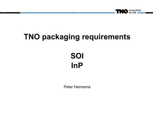
<strong>TNO</strong> packaging requirementsSOIInPPeter Harmsma
EUR 10,- for a package..??Low-cost componentsAs-cleaved fibersNo TECAll processing at wafer levelNo die-wise polishing stepsAlignment tolerantFiber-matched out-of-plane grating couplersCan be done
Feasibility study @ <strong>TNO</strong>Process developmentVarious concepts, grating coupler basedOnly fiber-chip subassemblyFiber-by-fiber for nowScalable to arraysNo signal loss after fixationSimulationsImpact of reflections for single-fiber assembliesTool conceptWhat tool is needed to produce 100.000 /yearWhat degree of automation makes senseWhat is the cost per device
Participation in PARADIGMInP enables more functionalityOn-board sources & detectorsAmplificationPerformancePrice of die is higher…… but not much. Packaging costs are dominantSize of circuit is larger…… a 50x50 um SOI circuit needs 1 mm 2 for packagingInP packaging more expensive than SOI packagingTypically Spot Size Converters + lensed fiberMainly for advanced applicationsRF, thermal, …, makes packaging even more expensiveInP for single-use sensors not an option
<strong>TNO</strong> needs for PARADIGMGeneral requirement: accurate thermal controlMain componentSingle optical I/O> 20 Multiple electrical I/O, < 50 kHz‘If it fits we put it on’ componentsDual / triple optical I/OFew electrical I/O (
What for the futureMore optical I/OOptical isolator / polarization manipulationMore electrical I/O (polarization diversity: x2?)In-package electronicsTIAsElectrical serialization