Trends in Lithography - JePPIX
Trends in Lithography - JePPIX
Trends in Lithography - JePPIX

You also want an ePaper? Increase the reach of your titles
YUMPU automatically turns print PDFs into web optimized ePapers that Google loves.
<strong>Lithography</strong><br />
Rob Hartman<br />
Symposium on Photonic Integration, 9 November 2011, TU/e<br />
Public
Outl<strong>in</strong>e<br />
• ASML<br />
• KennisWerkersRegel<strong>in</strong>g<br />
• PAS 5500 /1150C<br />
Public
Outl<strong>in</strong>e<br />
• ASML<br />
• KennisWerkersRegel<strong>in</strong>g<br />
• PAS 5500 /1150C<br />
Public
From silicon to smart electronics<br />
$6.1 B<br />
Semiconductor<br />
Litho market <strong>in</strong> 2010<br />
$2.5 B <strong>in</strong> 2009<br />
Source: Gartner Q3/10 and ASML<br />
$1,360 B Electronic Applications <strong>in</strong> 2010<br />
$1,204 B <strong>in</strong> 2009<br />
Public<br />
$300.3 B<br />
Semiconductor<br />
Chips <strong>in</strong> 2010<br />
$228.4 B <strong>in</strong> 2009
ASML Headquarters <strong>in</strong> Veldhoven<br />
Public
ASML number 2 worldwide<br />
semiconductor equipment vendor<br />
19%<br />
sales<br />
to US<br />
ASML employees<br />
<strong>in</strong> US:1,516<br />
Over 55 sales and service offices located worldwide<br />
Source: ASML Q3 2011<br />
ASML employees<br />
<strong>in</strong> Europe: 4,670<br />
Public<br />
9% sales<br />
to Europe<br />
72%<br />
sales<br />
to ASIA<br />
ASML employees<br />
<strong>in</strong> Asia:1,662
The economic benefit of ASML enabled<br />
Integrated Circuit Geometry reduction<br />
<strong>Lithography</strong> cost per unit of memory $/GByte<br />
10000<br />
1000<br />
100<br />
10<br />
1<br />
0<br />
KrF<br />
$1,162 for 1 Gigabyte (GB)<br />
ArF<br />
2000 2001 2002 2003 2004 2005 2006 2007 2008 2009 2010 2011 2012 2013 2014 2015<br />
Public<br />
Note: data iSuppli, March 2009. High quality Flash<br />
ArFi<br />
ArFi<br />
DPT<br />
EUV<br />
$0.17 for 1 GB<br />
600<br />
500<br />
400<br />
300<br />
200<br />
100<br />
0<br />
ASML R&D spend (€)
Net system sales breakdown <strong>in</strong> value: 2010<br />
Korea<br />
32%<br />
Region<br />
USA<br />
13%<br />
Taiwan<br />
32%<br />
Technology<br />
ArF KrF<br />
immersion 17%<br />
ArF 83%<br />
Immersion<br />
77%<br />
Europe 4%<br />
Japan 9%<br />
S<strong>in</strong>gapore 5%<br />
Ch<strong>in</strong>a 5%<br />
Public<br />
ArF dry 5%<br />
I-L<strong>in</strong>e 1%<br />
Numbers have been rounded for readers’ convenience.<br />
94<br />
ArF<br />
immersion<br />
End-use<br />
NAND<br />
19%<br />
DRAM<br />
47%<br />
Sales <strong>in</strong> Units<br />
12<br />
68<br />
Foundry 24%<br />
23<br />
ArF dry KrF I-L<strong>in</strong>e<br />
IDM 10%
ASML Q3 2011 results<br />
Q3 2011<br />
Net sales of € 1,457 million<br />
55 systems sold<br />
Net <strong>in</strong>come of € 355 million<br />
Q2 2011<br />
Net sales of € 1,529 million<br />
63 systems sold<br />
Net <strong>in</strong>come of € 432 million<br />
Full Year 2010<br />
Net sales of € 4,508 million<br />
197 systems sold<br />
Net <strong>in</strong>come of € 1,022 million<br />
Public<br />
Revenue<br />
worldwide Q3 2011<br />
Europe 9%<br />
US 19%<br />
Korea 24%<br />
Japan 13%<br />
S<strong>in</strong>gapore 13%<br />
Ch<strong>in</strong>a 15%<br />
Taiwan 7%
Outl<strong>in</strong>e<br />
• ASML<br />
• KennisWerkersRegel<strong>in</strong>g<br />
• PAS 5500 /1150C<br />
Public
Public<br />
• hoewel slechts 1 FTE heeft de<br />
KWR tot een <strong>in</strong>tensieve<br />
samenwerk<strong>in</strong>g geleid tussen<br />
ASML en TU/e<br />
• 17 maanden, ~ 160 k€ totale<br />
project kosten<br />
• mach<strong>in</strong>e aanpass<strong>in</strong>gen, <strong>in</strong> het<br />
bijzonder de chuck<br />
• NWO groot heeft de middelen<br />
beschikbaar gesteld om de<br />
mach<strong>in</strong>e aan te schaffen<br />
• KWR heeft ASML geïnspireerd<br />
om de komende 5 jaar te<br />
helpen met het onderhoud van<br />
de mach<strong>in</strong>e, vertegenwoordigd<br />
een waarde van 1.2 M €
Outl<strong>in</strong>e<br />
• ASML<br />
• KennisWerkersRegel<strong>in</strong>g<br />
• PAS 5500 /1150C<br />
Public
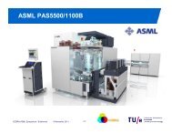
PAS 5500 /1150C<br />
200mm ArF Scanner
ASML <strong>Lithography</strong> Product Families<br />
Platform:<br />
System Type:<br />
Introduction:<br />
Wafer Size:<br />
Application:<br />
PAS 2500/5000<br />
Stepper<br />
1985<br />
≤ 150mm<br />
1.0 - 0.45µm<br />
Innovations: TTL DRR<br />
Phase Grat<strong>in</strong>g Align<br />
Air Bear<strong>in</strong>g<br />
L<strong>in</strong>ear Motor Stages<br />
Public<br />
PAS 5500<br />
Stepper / Scanner<br />
1990 / 1997<br />
100- 200mm<br />
0.50µm - 90 nm<br />
5-axis Stage Interferometry<br />
On-the-fly Focus & Level<strong>in</strong>g<br />
Magnetically Coupled<br />
Motor Scann<strong>in</strong>g stages<br />
TWINSCAN<br />
Scanner<br />
2000<br />
200 & 300mm<br />
0.15 -
Evolution of PAS 5500/1150C<br />
PAS 5500 /1100 /1100B /1150C<br />
Wavelength nm 193 193 193<br />
NA 0.75 - 0.50 0.75 - 0.50 0.75 - 0.50<br />
Resolution nm 100 100 90<br />
First Shipment Q2, 2001 Q3, 2002 Q2, 2003<br />
Illum<strong>in</strong>ation, Laser W 10 20 20<br />
Max. Intensity mW/cm 2<br />
270 850 1,100<br />
Overlay, S<strong>in</strong>gle Mach<strong>in</strong>e nm 20 15 12<br />
Overlay, Mach. to Mach. nm 30 25 20<br />
Throughput (OA) wph 90 120 135<br />
Dose mJ/cm 2<br />
20 20 20<br />
# Fields (16 x 32 mm 2 ) 46 46 46<br />
Scan Speed mm/s 250 250 320<br />
Lot Overhead s 20 20 20<br />
Options PEP1100<br />
IOSc-3 IOSc-3<br />
Public<br />
Resolution<br />
- 10%<br />
Overlay<br />
- 20%<br />
Productivity<br />
+ 12.5%
80 nm Dense L<strong>in</strong>es - Dipole<br />
F - 0.2 F - 0.1 F 0.0 F + 0.1 F + 0.2<br />
F - 0.25<br />
F - 0.3<br />
CD (nm)<br />
95<br />
90<br />
85<br />
80<br />
75<br />
70<br />
65<br />
60<br />
55<br />
50<br />
-0.60 -0.40 -0.20 0.00 0.20 0.40 0.60<br />
focus<br />
B<strong>in</strong>ary Mask Pitch = 160 nm<br />
NA = 0.75, σ = 0.88/0.64, Dipole<br />
Illum<strong>in</strong>ation<br />
Public<br />
Resist thickness = 210nm<br />
21.9<br />
22.2<br />
22.5<br />
22.8<br />
23.1<br />
23.4<br />
23.7<br />
24.0<br />
24.3<br />
24.6<br />
24.9<br />
25.2<br />
25.5<br />
25.8<br />
26.1<br />
F + 0.25<br />
F + 0.3
Improved Aberration Control<br />
PAS 5500 systems correct for<br />
• Magnification (lens manipulator)<br />
• Field curvature & astigmatism (lens manipulator)<br />
• 3 rd Order distortion (reticle height)<br />
PAS 5500 /1100 systems also correct for<br />
• Spherical aberration offset (lens manipulator)<br />
• Coma-tilt (<strong>in</strong>-l<strong>in</strong>e laser wavelength tun<strong>in</strong>g)<br />
Public
3DAlign TM is a patented revolutionary<br />
technology developed for the MEMS market<br />
Top<br />
Wafer<br />
Optical<br />
w<strong>in</strong>dows<br />
Lens<br />
Wafer table Optics<br />
Bottom<br />
Public<br />
Side View<br />
alignment marker<br />
Layer 2<br />
Layer 1<br />
Si<br />
FTBA<br />
New technology support<strong>in</strong>g<br />
the transition from contact<br />
aligners to reduction<br />
projection lithography
PAS 5500 Product Group serves<br />
Niche Markets - bridg<strong>in</strong>g the manufactur<strong>in</strong>g gap<br />
Image Sensors<br />
Bio chips<br />
Mechanical<br />
structures<br />
Products<br />
High Outgass<strong>in</strong>g<br />
aspect<br />
safeguards<br />
ratio<br />
Square wafer<br />
handl<strong>in</strong>g<br />
Public<br />
Small wafer<br />
handl<strong>in</strong>g<br />
Litho equipment<br />
Equipment Enabl<strong>in</strong>g Equipment Enabl<strong>in</strong>g Equipment Enabl<strong>in</strong>g<br />
adaptations<br />
processes adaptations<br />
processes adaptations<br />
processes<br />
Micro<br />
pipettes<br />
Special Optics<br />
CNT<br />
Small pieces<br />
handl<strong>in</strong>g<br />
T-gate gate process<br />
Back-side Back side wafer<br />
alignment<br />
Optical devices<br />
HB LEDs<br />
Fluidics
The PAS 5500 competence center <strong>in</strong> ACE (Taiwan)<br />
concentrates ≤200mm knowledge <strong>in</strong> one place<br />
The competence center offers dedicated resources for the PAS 5500<br />
platform<br />
It comb<strong>in</strong>es the know-how and skills of Development & Eng<strong>in</strong>eer<strong>in</strong>g,<br />
Manufactur<strong>in</strong>g and Customer Support <strong>in</strong> one eng<strong>in</strong>eer<strong>in</strong>g team<br />
The center will also benefit from the synergies with the other ACE<br />
activities (Tra<strong>in</strong><strong>in</strong>g, GSC-Tw<strong>in</strong>scan, Application development, Sourc<strong>in</strong>g)<br />
Total capital Investment > 25M€<br />
L<strong>in</strong>kou<br />
Public
PAS 5500 Systems and Services<br />
Refurbished Systems<br />
PAS 5500 Product Group provides (factory) refurbished systems to<br />
markets such as compound, opto electronic, mems, TFH as well as<br />
the still grow<strong>in</strong>g 8” logic and mixed signal fabs.<br />
Installed Base Support and Service<br />
The <strong>in</strong>stalled base of our 200mm customers is > 1800 systems and<br />
projected to run for a long time. PAS 5500 Product Group supports<br />
and enhances their <strong>in</strong>stalled base.<br />
Public
Technology Network for Competence Development<br />
ASML demo Lab at<br />
Stanford University<br />
SNF<br />
FP6<br />
Public<br />
ASML Appl.<br />
Dev. Lab<br />
Netherlands<br />
COBRA<br />
DIMES