Phys. Rev. Lett. 90, 177402 - Physik-Institut
Phys. Rev. Lett. 90, 177402 - Physik-Institut
Phys. Rev. Lett. 90, 177402 - Physik-Institut

You also want an ePaper? Increase the reach of your titles
YUMPU automatically turns print PDFs into web optimized ePapers that Google loves.
VOLUME <strong>90</strong>, NUMBER 17<br />
PHYSICAL REVIEW LETTERS week ending<br />
2 MAY 2003<br />
Optical Recognition of Atomic Steps on Surfaces<br />
F. Baumberger, 1 Th. Herrmann, 2 A. Kara, 3 S. Stolbov, 3 N. Esser, 2 T. S. Rahman, 3 J. Osterwalder, 1<br />
W. Richter, 2 and T. Greber 1<br />
1 <strong>Phys</strong>ik <strong>Institut</strong> der Universität Zürich, Winterthurerstrasse 1<strong>90</strong>, CH-8057 Zürich, Switzerland<br />
2 <strong>Institut</strong> für Festkörperphysik der TU Berlin, Hardenbergstrasse 36, D-10623 Berlin, Germany<br />
3 Department of <strong>Phys</strong>ics, Cardwell Hall, Kansas State University, Manhattan, Kansas 66506<br />
(Received 3 November 2002; published 29 April 2003)<br />
Visible and UV light spectra display striking differences in optical reflectivity for the two types of<br />
monatomic steps on copper (111) surfaces. Electronic structure calculations trace these differences to<br />
the specific contributions of p k and p ? local densities of states, parallel and perpendicular to the steps,<br />
of the distinctly coordinated corner atoms. The local origin of the spectral reflectance anisotropy is<br />
further corroborated by experiments on Cu(111) surfaces with varying step densities. Site specificity of<br />
the electronic structure of atoms in low coordinated sites on Cu(111) vicinals is thus revealed by<br />
reflectance anisotropy spectroscopy which can thereby detect step atom densities down to<br />
10 13 atoms=cm 2 .<br />
DOI: 10.1103/<strong>Phys</strong><strong>Rev</strong><strong>Lett</strong>.<strong>90</strong>.<strong>177402</strong><br />
PACS numbers: 78.40.–q, 68.37.–d, 73.20.–r, 82.45.Jn<br />
Steps break the symmetry of surfaces which leads to a<br />
number of unique functionalities. The low coordinated<br />
atoms at steps are key players in heterogeneous catalysis<br />
[1–3], tribology [4], epitaxial growth [5], and the formation<br />
of molecular nanostructures [6]. The complex geometry<br />
of a stepped surface offers local environments of<br />
varying atomic coordination. Take, for example, steps on<br />
an otherwise flat hexagonal surface. Atoms on the flat<br />
surface have a coordination (number of nearest neighbors)<br />
of 9, while creation of a monoatomic step on this surface<br />
will produce atoms with coordination ranging from 7<br />
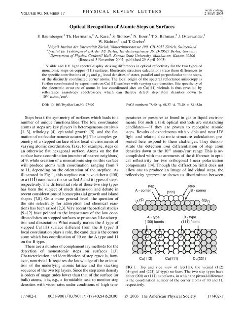
to 11, depending on the orientation of the stepface. As<br />
illustrated in Fig. 1, this stepface can have either a (100)<br />
or a 111 nanofacet: the so-called A and B types of steps,<br />
respectively. The differential role of these two step types<br />
has been the subject of much discussion and debate in<br />
recent considerations of homoepitaxial growth and island<br />
shapes [7,8]. On a more general level, the question of<br />
the site selectivity for adsorption and chemical reactions<br />
has been raised [2,3]. Very recent theoretical studies<br />
[9–12] have pointed to the importance of the low coordinated<br />
sites on stepped surfaces to processes like adsorption<br />
and dissociation. What exactly makes the A type of<br />
stepped Cu(111) surface different from the B type? If<br />
local coordination plays a role, the candidate is the corner<br />
atom which has coordination of 10 on the A type and 11<br />
on the B type.<br />
There are a number of complementary methods for the<br />
detection of monoatomic steps on surfaces [13].<br />
Characterization and identification of step types is, however,<br />
nontrivial. It requires the knowledge of the orientation<br />
of the underlying atomic lattice and the stacking<br />
sequence of the two top layers. Since the step atom density<br />
is orders of magnitudes lower than that of the surface (or<br />
bulk) atoms, it is, e.g., a formidable task to monitor step<br />
densities with video rates under conditions of high temperatures<br />
or pressures as found in gas or liquid environments.<br />
For such a task optical methods are outstanding<br />
candidates — if they are proven to recognize atomic<br />
steps. Results of experiments with visible and near UV<br />
light and related electronic structure calculations presented<br />
here respond to these challenges. They demonstrate<br />
the detection and differentiation of step atom<br />
densities down to the 10 13 atoms=cm 2 range. This is accomplished<br />
with measurements of the difference in optical<br />
reflectivity for two orthogonal linear polarization<br />
components [14]. Though the diffraction limit does not<br />
allow one to produce an image of individual steps, the<br />
reflectivity spectra are shown to discriminate between<br />
step<br />
A - corner<br />
(112)<br />
A - type<br />
(100) facets<br />
Cu(112)<br />
(111)<br />
Cu(111)<br />
step<br />
B - corner<br />
B type<br />
-<br />
(111) facets<br />
(221)<br />
Cu(221)<br />
FIG. 1. Top and side view of fcc(111), the vicinal (112)<br />
(A-type) and (221) (B-type) surfaces. The two step types have<br />
either (001) or 111 nanofacets, in which the pivotal difference<br />
is the coordination number of the corner atoms of 10 and 11,<br />
respectively.<br />
<strong>177402</strong>-1 0031-<strong>90</strong>07=03=<strong>90</strong>(17)=<strong>177402</strong>(4)$20.00 © 2003 The American <strong>Phys</strong>ical Society <strong>177402</strong>-1
VOLUME <strong>90</strong>, NUMBER 17<br />
PHYSICAL REVIEW LETTERS week ending<br />
2 MAY 2003<br />
the two different step types (A and B) on vicinal hexagonally<br />
close-packed metal surfaces. Accompanying theoretical<br />
calculations trace this difference in the A- and<br />
B-type steps to the anisotropy of the partial local density<br />
of states (LDOS) of the corner atoms on the two surfaces.<br />
Reflectance anisotropy spectroscopy (RAS) is a nondestructive,<br />
noninvasive method that has been developed<br />
by Aspnes et al. [14] and was put forward by the fact that<br />
the linear optical response of a cubic crystal is isotropic<br />
in the bulk, and any deviation from zero in the signal<br />
can be interpreted as a signature of the electronic structure<br />
of the surface [14]. So far RAS has been applied to<br />
semiconductors [15,16] and to metallic fcc surfaces [17–<br />
20]. This <strong>Lett</strong>er reports the application of RAS to a<br />
number of vicinal surfaces of copper which, together<br />
with related ab initio electronic structure calculations,<br />
enables an unambiguous optical discrimination between<br />
A- andB-type steps.<br />
The experiments were performed under ultrahigh<br />
vacuum conditions where the crystals were prepared<br />
and characterized with standard procedures that show<br />
clean surfaces with monoatomic steps [21]. Near normal<br />
RAS measurements were taken with a mobile spectrometer<br />
[22] through a low strain quartz window in<br />
the spectral range between 0.8 and 6.5 eV. The reflectance<br />
anisotropy (RA) is defined as the real part of the<br />
difference in the Fresnel reflectance amplitudes for two<br />
orthogonal directions of the light polarization, parallel<br />
and perpendicular to the steps, normalized with the mean<br />
reflectance RA 2Re r k r ? = r k r ? .<br />
Figure 1 depicts two of the investigated vicinal fcc(111)<br />
surfaces. The steps run along the close-packed 110<br />
direction and their density is controlled by the miscut<br />
angle relative to the [111] direction. A-type Cu(112) has<br />
one (100) nanofacet and one terrace atom per unit cell<br />
while B-type Cu(221) has one 111 facet and two terrace<br />
atoms.<br />
Experimental reflectance anisotropy spectra for<br />
Cu(112) and Cu(221) are shown in Fig. 2. Above 2 eV<br />
anisotropic interband transitions that determine the color<br />
of copper set in, and at 4.3 eV, both types of vicinals show<br />
a well resolved, shoulder free peak which is a maximum<br />
in the spectrum for the A type and a minimum for the B<br />
type. Thus the reflectivity along the steps at 4.3 eV is<br />
enhanced (reduced) for the A (B) type. This signature<br />
clearly discriminates the two types of surfaces.<br />
On Cu(110) a similar RA minimum at 4.3 eV was<br />
reported [18,23,24]. This resemblance between the<br />
B-type vicinals and the (110) surface is appealing since<br />
the top layer and the second layer atoms on fcc(110) have<br />
a coordination of 7 and 11, just as the step and corner<br />
atoms on the B-type vicinals. This is to be contrasted with<br />
the distinct atomic structure and coordination of the A<br />
type: the step nanofacet presents an open (100) geometry<br />
with the step atoms still having a coordination of 7, but<br />
the corner atoms have a coordination of 10.<br />
Reflectance Anisotropy (10 -3 )<br />
2<br />
1<br />
2 3 4 5<br />
Photon Energy (eV)<br />
A - type<br />
Cu(112)<br />
B - type<br />
Cu(221)<br />
FIG. 2. Near normal reflectance anisotropy for Cu(112) and<br />
Cu(221), as a function of photon energy.<br />
We have calculated the electronic structure of A-type<br />
Cu(112) and B-type Cu(331) with one terrace atom per<br />
unit cell using density functional theory in the local<br />
density approximation and multiple scattering theory in<br />
the framework of the local self-consistent multiple scattering<br />
method [25]. This is a local approach performed in<br />
the real space and hence it provides detailed information<br />
about the local electronic states at atomic sites with different<br />
environment. Analysis of the s, p, andd LDOS of<br />
the surface atoms reveals that the p states are most likely<br />
to be at the origin of the anisotropies of the A-andB-type<br />
vicinals observed in the spectra. Moreover, the different<br />
signs of the anisotropy at 4.3 eV can be explained by<br />
interband transitions involving the corner atom.<br />
Optical anisotropy implies optical transitions and a<br />
difference in the corresponding partial LDOS of the initial<br />
and/or final states. In Fig. 3(a) the difference in the<br />
local density of p states parallel and perpendicular to the<br />
steps p k p ? is shown for the A- andB-type vicinals. It<br />
gives the sources of possible anisotropies in either the<br />
initial or final states of the transitions. However, not all<br />
positions in this spectrum contribute to optical transitions.<br />
In order to obtain the optical anisotropy this partial<br />
LDOS difference has to be weighted with the optical<br />
transition probability. For bulk copper a strong optical<br />
excitation at 4.3 eV is assigned to p ! s interband transitions<br />
where the p derived states are located just above<br />
the d band, at a binding energy of 1eV[26] [see the<br />
inset in Fig. 3(a)]. The calculated difference in the partial<br />
local density of states p k p ? for Cu(112) and<br />
Cu(331) at 1 eV indeed reflects this anisotropy in the<br />
region below the Fermi level. More strikingly, we find<br />
6<br />
7<br />
<strong>177402</strong>-2 <strong>177402</strong>-2
VOLUME <strong>90</strong>, NUMBER 17<br />
(a)<br />
(b)<br />
p // - p⊥ DOS (states/eV)<br />
p // - p⊥ LDOS (states/eV)<br />
0.08<br />
0.04<br />
0.00<br />
-0.04<br />
0.002<br />
0.000<br />
-0.002<br />
d → p<br />
8 4 0 -4<br />
E B (eV)<br />
1 2 3 4 5 6 7 8 9 10<br />
Layer # (n)<br />
p → s<br />
Cu(112)<br />
Cu(331)<br />
Cu(112)<br />
Cu(331)<br />
FIG. 3. (a) Total anisotropy of the partial local density of<br />
states (p k p ? ) for the top ten layers of Cu(112) and Cu(331).<br />
The inset zooms into the spectrum where the p ! s (4.3 eV)<br />
and the d ! p (2 eV) interband transitions occur [26].<br />
(b) Layer resolved anisotropy of the p LDOS at a binding<br />
energy of 1 eV. The layers are numbered along the vicinal<br />
planes, starting from the outermost step atom (n 1).<br />
Layer 3 corresponds to the corner atoms.<br />
an opposite anisotropy for the A-andB-type vicinals, just<br />
as in the experimental reflectivity curves at 4.3 eV photon<br />
energy, shown in Fig. 2 and the sign of p k p ? agrees<br />
with the experimental reflectance anisotropy.<br />
In order to identify the corner atoms as the main contribution<br />
to the 4.3 eV anisotropy difference, we plot in<br />
Fig. 3(b) the p k p ? LDOS, at a binding energy of<br />
1eV for the different layers (atoms) n on the two<br />
vicinals. Indeed, the difference in the anisotropy has its<br />
largest contribution from the corner atoms of the A- and<br />
B-type steps (n 3). Figure 3(b) is also indicative of the<br />
degree of localization of the anisotropy. It decays exponentially<br />
away from the corner atoms and the screening<br />
length is of the order of the Fermi wavelength (4:6 A for<br />
copper).<br />
The assignment to a local origin (corner atoms) of the<br />
4.3 eV reflectance anisotropy is further corroborated by<br />
PHYSICAL REVIEW LETTERS week ending<br />
2 MAY 2003<br />
E F<br />
x 3<br />
the analysis of Cu(332) and Cu(443), i.e., two more<br />
B-type surfaces with different step densities. Figure 4<br />
shows that the anisotropy of the peak at 4.3 eV is roughly<br />
proportional to the step density 1=‘, where ‘ is the step<br />
separation length. The proportionality factor is about<br />
7:5 0:8 10 3 ‘ o , where ‘ 3 o is the atomic volume.<br />
With a penetration depth of 80‘ o for 4.3 eV photons into<br />
copper we see that the observed anisotropy may have a<br />
local origin, i.e., have its source in single atomic objects<br />
on the surface. The proportionality factor for the measured<br />
A type has opposite sign, though the same order of<br />
magnitude. The sensitivity for the reflection anisotropy in<br />
the current setup is estimated to 0:5 10 3 [27] and<br />
translates for a given orientation on vicinal copper into a<br />
step density 1=‘ of 10 6 steps=cm or a step atom density<br />
1=‘‘ o of 5 10 13 step atoms=cm 2 .<br />
Besides the previously discussed 4.3 eV feature, the<br />
reflectance anisotropy spectra contain a signature at<br />
2eV which does not change sign between A- and<br />
B-type vicinals but is in intensity proportional to the<br />
step density, too. In contrast to Cu(110) where at this<br />
energy a resonance of the highly anisotropic Shockley<br />
surface state with an unoccupied surface state occurs [18],<br />
no influence of the Shockley surface state was found.<br />
Experiments where the surfaces were exposed to oxygen<br />
and ambient air showed the reflectance anisotropy spectra<br />
to be susceptible to oxidation, though in the whole observed<br />
photon energy range no spectral feature could be<br />
assigned to the disappearance of the Shockley surface<br />
state. However, distinct signatures from the A and B types<br />
that reconstruct differently under oxygen exposure<br />
[28,29] persist and give further evidence for the usefulness<br />
of RAS. If, however, the above theoretical analysis is<br />
performed for optical excitations at 2eV, i.e., the<br />
d ! p transitions, we find in this case the step atoms<br />
(n 1) to contribute the main anisotropy in the relevant<br />
unoccupied p states above the Fermi level [26]. The<br />
anisotropies have the same sign and magnitude for A<br />
and B types and are in line with the same coordination<br />
for A- andB-type step atoms [30].<br />
From the trace back of the optical anisotropies to<br />
differently coordinated atoms we conjecture that such<br />
step signatures should be generally found on stepped<br />
surfaces. On a given vicinal fcc(111) surface the two<br />
different anisotropies from the corner and the step atoms<br />
provide the unique opportunity to determine the nature,<br />
orientation, and concentration of steps by recording<br />
reflectance anisotropy spectra for different azimuthal<br />
angles of the polarization planes of the incoming light.<br />
In summary it is shown that RAS provides information<br />
from which it is possible to recognize very low<br />
densities of differently coordinated atoms on surfaces.<br />
Furthermore, ab initio electronic structure calculations<br />
are able to identify the local characteristics that distinguish<br />
the atoms in low coordinated sites on stepped<br />
surfaces. These results open the way for detailed<br />
<strong>177402</strong>-3 <strong>177402</strong>-3
VOLUME <strong>90</strong>, NUMBER 17<br />
Reflectance Anisotropy (10 -3 )<br />
4<br />
2<br />
0<br />
-2<br />
-4<br />
0.0<br />
A - type<br />
B - type<br />
0.1<br />
1/ (Å -1 )<br />
0.2<br />
FIG. 4. Reflectance anisotropy at 4.3 eV for Cu(112) (square),<br />
Cu(111) (circle), and Cu(443), Cu(332), and Cu(221) (triangles)<br />
as a function of the step density 1=‘, where ‘ is the step-step<br />
separation.<br />
investigations of site selectivity in various physical and<br />
chemical processes on heterogeneous surfaces. The findings<br />
also provide the opportunity for the exploitation of<br />
this effect in optical microscopes with spectral discrimination.<br />
Applications, such as the online control of the<br />
microscopic roughness in epitaxy or its correlation with<br />
catalytic activity can be realized.<br />
This work has been supported by the Swiss National<br />
Science Foundation and the SFB 2<strong>90</strong> of the Deutsche<br />
Forschungsgemeinschaft (DFG). A. K., S. S., and T. S. R<br />
are supported by the U.S. Basic Energy Research<br />
Division, Department of Energy, Grant No. DE-FG03-<br />
97ER45650. A. K. thanks his colleagues at the University<br />
of Zürich for their warm hospitality. Fruitful discussions<br />
with Ph. Hofmann and L. Mochan are gratefully<br />
acknowledged.<br />
[1] G. A. Somorjai, Surface Chemistry and Catalysis (Wiley<br />
& Sons, New York, 1994).<br />
[2] T. Zambelli, J. Wintterlin, J. Trost, and G. Ertl, Science<br />
273, 1688 (1996).<br />
[3] L. M. Falicov and G. A. Somorjai, Proc. Natl. Acad. Sci.<br />
U.S.A. 82, 2207 (1985).<br />
[4] B. N. J. Persson, Sliding Friction: <strong>Phys</strong>ical Principles<br />
and Applications (Springer, Berlin, Heidelberg, 1998).<br />
[5] A. Zangwill, <strong>Phys</strong>ics at Surfaces (Cambridge University<br />
Press, Cambridge, 1988).<br />
[6] R. Fasel, A. Cossy, K. H. Ernst, F. Baumberger, T. Greber,<br />
and J. Osterwalder, J. Chem. <strong>Phys</strong>. 115, 1020 (2001).<br />
PHYSICAL REVIEW LETTERS week ending<br />
2 MAY 2003<br />
[7] T. Michely, M. Hohage, M. Bott, and G. Comsa, <strong>Phys</strong>.<br />
<strong>Rev</strong>. <strong>Lett</strong>. 70, 3943 (1993).<br />
[8] C. Steimer, M. Giesen, L. Verheij, and H. Ibach, <strong>Phys</strong>.<br />
<strong>Rev</strong>. B 64, 085416 (2001).<br />
[9] B. Hammer and J. K. Nørskov, <strong>Phys</strong>. <strong>Rev</strong>. <strong>Lett</strong>. 79, 4441<br />
(1997).<br />
[10] B. Hammer, <strong>Phys</strong>. <strong>Rev</strong>. <strong>Lett</strong>. 83, 3681 (1999).<br />
[11] P. Gambardella, Z. Sljivancanin, B. Hammer, M. Blanc,<br />
K. Kuhnke, and K. Kern, <strong>Phys</strong>. <strong>Rev</strong>. <strong>Lett</strong>. 87, 056103<br />
(2001).<br />
[12] I. Makkonen, P. Salo, M. Alatalo, and T. S. Rahman,<br />
<strong>Phys</strong>. <strong>Rev</strong>. B (to be published).<br />
[13] H.-C. Jeong and E. D. Williams, Surf. Sci. Rep. 34, 175<br />
(1999), and references therein.<br />
[14] D. E. Aspnes, J. P. Harbison, A. A. Studna, and L. T.<br />
Florez, J. Vac. Sci. Technol. A 6, 1327 (1988).<br />
[15] I. Kamiya, D. E. Aspnes, H. Tanaka, L.T. Florez, J. P.<br />
Harbison, and R. Bhat, <strong>Phys</strong>. <strong>Rev</strong>. <strong>Lett</strong>. 68, 627 (1992).<br />
[16] A. I. Shkrebtii, N. Esser, W. Richter, W. G. Schmidt,<br />
F. Bechstedt, B. O. Fimland, A. Kley, and R. Del Sole,<br />
<strong>Phys</strong>. <strong>Rev</strong>. <strong>Lett</strong>. 81, 721 (1998).<br />
[17] Y. Borensztein, W. L. Mochan, J. Tarriba, R. G. Barrera,<br />
and A. Tadjeddine, <strong>Phys</strong>. <strong>Rev</strong>. <strong>Lett</strong>. 71, 2334 (1993).<br />
[18] Ph. Hofmann, K. C. Rose, V. Fernandez, A. M. Bradshaw,<br />
and W. Richter, <strong>Phys</strong>. <strong>Rev</strong>. <strong>Lett</strong>. 75, 2039 (1995).<br />
[19] A. Borg, O. Hunderi, W. Richter, J. Rumberg, and H. J.<br />
Venvik, <strong>Phys</strong>. Status Solidi (a) 152, 77 (1995).<br />
[20] V. Mazine and Y. Borensztein, <strong>Phys</strong>. <strong>Rev</strong>. <strong>Lett</strong>. 88,<br />
147403 (2002).<br />
[21] F. Baumberger, T. Greber, and J. Osterwalder, <strong>Phys</strong>.<br />
<strong>Rev</strong>. B 64, 195411 (2001).<br />
[22] W. Richter and J.-T. Zettler, Appl. Surf. Sci.. 101, 465<br />
(1996).<br />
[23] K. Stahrenberg, Th. Herrmann, N. Esser, and W. Richter,<br />
<strong>Phys</strong>. <strong>Rev</strong>. B 61, 3043 (2000).<br />
[24] J.-K. Hansen, J. Bremer, and O. Hunderi, Surf. Sci. 418,<br />
L58 (1998).<br />
[25] Y. Wang, G. M. Stocks,W. A. Shelton, D. M. C. Nicholson,<br />
Z. Szotek, and W. M. Temmerman, <strong>Phys</strong>. <strong>Rev</strong>. <strong>Lett</strong>. 75,<br />
2867 (1995).<br />
[26] K. Stahrenberg, Th. Herrmann, K. Wilmers, N. Esser,<br />
W. Richter, and M. J. G. Lee, <strong>Phys</strong>. <strong>Rev</strong>. B 64, 115111<br />
(2001).<br />
[27] This estimate for the sensitivity is taken from the scatter<br />
of the data around the =‘ line for the four individual<br />
B-type samples (see Fig. 4). From the data in Fig. 2 it can<br />
be seen that the RA signal from a given surface may be<br />
measured with a much higher accuracy. Therefore on a<br />
given sample significant RA changes in the 10 4 range<br />
may be detected.<br />
[28] G. Witte, J. Braun, D. Nowack, L. Bartels, B. Neu, and<br />
G. Meyer, <strong>Phys</strong>. <strong>Rev</strong>. B 58, 13 224 (1998).<br />
[29] S. Vollmer, A. Birkner, S. Lukas, G. Witte, and Ch. Wöll,<br />
Appl. <strong>Phys</strong>. <strong>Lett</strong>. 76, 2686 (2000).<br />
[30] A. Kara et al. (to be published).<br />
<strong>177402</strong>-4 <strong>177402</strong>-4