Phys. Rev. Lett. 90, 177402 - Physik-Institut
Phys. Rev. Lett. 90, 177402 - Physik-Institut
Phys. Rev. Lett. 90, 177402 - Physik-Institut

Create successful ePaper yourself
Turn your PDF publications into a flip-book with our unique Google optimized e-Paper software.
VOLUME <strong>90</strong>, NUMBER 17<br />
PHYSICAL REVIEW LETTERS week ending<br />
2 MAY 2003<br />
the two different step types (A and B) on vicinal hexagonally<br />
close-packed metal surfaces. Accompanying theoretical<br />
calculations trace this difference in the A- and<br />
B-type steps to the anisotropy of the partial local density<br />
of states (LDOS) of the corner atoms on the two surfaces.<br />
Reflectance anisotropy spectroscopy (RAS) is a nondestructive,<br />
noninvasive method that has been developed<br />
by Aspnes et al. [14] and was put forward by the fact that<br />
the linear optical response of a cubic crystal is isotropic<br />
in the bulk, and any deviation from zero in the signal<br />
can be interpreted as a signature of the electronic structure<br />
of the surface [14]. So far RAS has been applied to<br />
semiconductors [15,16] and to metallic fcc surfaces [17–<br />
20]. This <strong>Lett</strong>er reports the application of RAS to a<br />
number of vicinal surfaces of copper which, together<br />
with related ab initio electronic structure calculations,<br />
enables an unambiguous optical discrimination between<br />
A- andB-type steps.<br />
The experiments were performed under ultrahigh<br />
vacuum conditions where the crystals were prepared<br />
and characterized with standard procedures that show<br />
clean surfaces with monoatomic steps [21]. Near normal<br />
RAS measurements were taken with a mobile spectrometer<br />
[22] through a low strain quartz window in<br />
the spectral range between 0.8 and 6.5 eV. The reflectance<br />
anisotropy (RA) is defined as the real part of the<br />
difference in the Fresnel reflectance amplitudes for two<br />
orthogonal directions of the light polarization, parallel<br />
and perpendicular to the steps, normalized with the mean<br />
reflectance RA 2Re r k r ? = r k r ? .<br />
Figure 1 depicts two of the investigated vicinal fcc(111)<br />
surfaces. The steps run along the close-packed 110<br />
direction and their density is controlled by the miscut<br />
angle relative to the [111] direction. A-type Cu(112) has<br />
one (100) nanofacet and one terrace atom per unit cell<br />
while B-type Cu(221) has one 111 facet and two terrace<br />
atoms.<br />
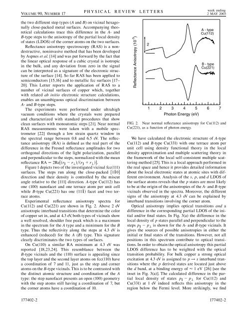
Experimental reflectance anisotropy spectra for<br />
Cu(112) and Cu(221) are shown in Fig. 2. Above 2 eV<br />
anisotropic interband transitions that determine the color<br />
of copper set in, and at 4.3 eV, both types of vicinals show<br />
a well resolved, shoulder free peak which is a maximum<br />
in the spectrum for the A type and a minimum for the B<br />
type. Thus the reflectivity along the steps at 4.3 eV is<br />
enhanced (reduced) for the A (B) type. This signature<br />
clearly discriminates the two types of surfaces.<br />
On Cu(110) a similar RA minimum at 4.3 eV was<br />
reported [18,23,24]. This resemblance between the<br />
B-type vicinals and the (110) surface is appealing since<br />
the top layer and the second layer atoms on fcc(110) have<br />
a coordination of 7 and 11, just as the step and corner<br />
atoms on the B-type vicinals. This is to be contrasted with<br />
the distinct atomic structure and coordination of the A<br />
type: the step nanofacet presents an open (100) geometry<br />
with the step atoms still having a coordination of 7, but<br />
the corner atoms have a coordination of 10.<br />
Reflectance Anisotropy (10 -3 )<br />
2<br />
1<br />
2 3 4 5<br />
Photon Energy (eV)<br />
A - type<br />
Cu(112)<br />
B - type<br />
Cu(221)<br />
FIG. 2. Near normal reflectance anisotropy for Cu(112) and<br />
Cu(221), as a function of photon energy.<br />
We have calculated the electronic structure of A-type<br />
Cu(112) and B-type Cu(331) with one terrace atom per<br />
unit cell using density functional theory in the local<br />
density approximation and multiple scattering theory in<br />
the framework of the local self-consistent multiple scattering<br />
method [25]. This is a local approach performed in<br />
the real space and hence it provides detailed information<br />
about the local electronic states at atomic sites with different<br />
environment. Analysis of the s, p, andd LDOS of<br />
the surface atoms reveals that the p states are most likely<br />
to be at the origin of the anisotropies of the A-andB-type<br />
vicinals observed in the spectra. Moreover, the different<br />
signs of the anisotropy at 4.3 eV can be explained by<br />
interband transitions involving the corner atom.<br />
Optical anisotropy implies optical transitions and a<br />
difference in the corresponding partial LDOS of the initial<br />
and/or final states. In Fig. 3(a) the difference in the<br />
local density of p states parallel and perpendicular to the<br />
steps p k p ? is shown for the A- andB-type vicinals. It<br />
gives the sources of possible anisotropies in either the<br />
initial or final states of the transitions. However, not all<br />
positions in this spectrum contribute to optical transitions.<br />
In order to obtain the optical anisotropy this partial<br />
LDOS difference has to be weighted with the optical<br />
transition probability. For bulk copper a strong optical<br />
excitation at 4.3 eV is assigned to p ! s interband transitions<br />
where the p derived states are located just above<br />
the d band, at a binding energy of 1eV[26] [see the<br />
inset in Fig. 3(a)]. The calculated difference in the partial<br />
local density of states p k p ? for Cu(112) and<br />
Cu(331) at 1 eV indeed reflects this anisotropy in the<br />
region below the Fermi level. More strikingly, we find<br />
6<br />
7<br />
<strong>177402</strong>-2 <strong>177402</strong>-2