characterization of group-iii nitride semiconductors by x-ray ... - Rigaku
characterization of group-iii nitride semiconductors by x-ray ... - Rigaku
characterization of group-iii nitride semiconductors by x-ray ... - Rigaku

Create successful ePaper yourself
Turn your PDF publications into a flip-book with our unique Google optimized e-Paper software.
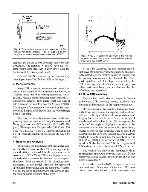
Fig. 3. Temperature sequence for deposition <strong>of</strong> AlN<br />
without nitridation process. NH 3 is supplied to the<br />
sapphire surface at temperatures lower than 800EC.<br />
respectively and are cooled down just before the AlN<br />
deposition. The samples and have the lowtemperature<br />
deposited AlN buffer layer with the<br />
thickness <strong>of</strong> 30 D (designed value).<br />
GaN and GaInN layers were grown continuously<br />
after deposition <strong>of</strong> 300 D-thick AlN buffer layer.<br />
3. Measurements<br />
X-<strong>ray</strong> CTR scattering measurements were conducted<br />
at the beam line BL6A in the Photon Factory in<br />
Tsukuba using the Weissenberg camera (R-AXIS-<br />
RAPID, <strong>Rigaku</strong>) and the imaging plate (IP) as the 2-<br />
dimensional detector. The camera length was fixed at<br />
286.5 mm and the wavelength <strong>of</strong> the X-<strong>ray</strong> at 1.600 D.<br />
The angle ω <strong>of</strong> the sample was scanned in the range<br />
between 2E higher and 8E lower than the (0006) Bragg<br />
point <strong>of</strong> sapphire.<br />
The X-<strong>ray</strong> reflectivity measurements in the low<br />
glancing angle was conducted using the conventional<br />
X-<strong>ray</strong> generator and diffractometer (RUH-450, <strong>Rigaku</strong>).<br />
The target was Cu operated at 35 kV with 330<br />
mA. The Cu K αl (λ=1.54056 D) line was chosen using<br />
Si(111) monochromator. The receiving slit was 0.05<br />
mm.<br />
4. Results and Analysis<br />
The process for the analysis <strong>of</strong> the measured data<br />
is basically the same for the CTR scattering and for<br />
the reflectivity. 1) A model for the layer structure is<br />
constructed. 2) The X-<strong>ray</strong> CTR scattering spectrum or<br />
the reflectivity spectrum is generated <strong>by</strong> a computer<br />
simulation from the model. 3) By changing those<br />
parameters in the model structure the generated<br />
spectra and the measured data are compared. 4) At the<br />
best fit, the set <strong>of</strong> parameters are considered to give<br />
the most probable structure <strong>of</strong> the layer.<br />
Fig. 4. X-<strong>ray</strong> CTR scattering spectrum <strong>of</strong> the <strong>nitride</strong>d<br />
sapphire surface. Dots are the measured data and the<br />
g<strong>ray</strong> line is the best fit curve.<br />
In the CTR scattering, the atom arrangements in<br />
each layer are the primary information to be obtained.<br />
In the reflectivity, the electron density in each layer is<br />
the primary information to be obtained. Therefore,<br />
good crystalline part <strong>of</strong> the layer is detected <strong>by</strong> the<br />
CTR scattering, and all <strong>of</strong> the crystalline, polycrystalline<br />
and amorphous part are detected <strong>by</strong> the<br />
reflectivity mea surements.<br />
4.1. X-<strong>ray</strong> CTR scattering<br />
The samples ˛ and ˇ showed no specific features<br />
in the X-<strong>ray</strong> CTR scattering spectra, i.e., those were<br />
the same as the spectrum <strong>of</strong> the sapphire substrate.<br />
On the other hand, the sample — had a clear bump<br />
in the lower angle side <strong>of</strong> the sapphire peak as shown<br />
in Fig. 4. In the figure dots are the measured data and<br />
the g<strong>ray</strong> line is the best fit curve. Since the sample —<br />
was the <strong>nitride</strong>d sapphire in the NH 3 atmosphere, the<br />
surface <strong>of</strong> the sapphire (Al 2 O 3 ) is considered to be<br />
converted to AlN. For the analysis <strong>by</strong> curve fitting,<br />
several possible model structures were as sumed; Al<br />
in AlN is bonded to Al or O in sapphire, or N in AlN is<br />
bonded to Al or O in sapphire, the polarity <strong>of</strong> AlN is<br />
[0001]A or [0001]B, the top surface <strong>of</strong> AlN is covered<br />
<strong>by</strong> Al or N, the thickness <strong>of</strong> AlN, the roughness <strong>of</strong><br />
AlN surface, the lattice distortion <strong>of</strong> AlN, and so on.<br />
The results <strong>of</strong> the analysis are illustrated in Fig 5.<br />
The thickness <strong>of</strong> the AlN layer was 3ML (7.47 D), the<br />
polarity was [0001]A, and the top surface <strong>of</strong> AlN was<br />
mostly covered <strong>by</strong> N.<br />
In the other samples - , the spectra were not<br />
clear and good fitting was not obtained. We considered<br />
that amorphous-like AlN containing fine<br />
56 The <strong>Rigaku</strong> Journal