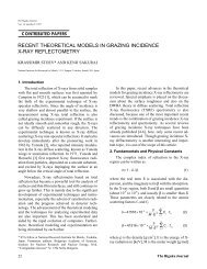
characterization of group-iii nitride semiconductors by x-ray ... - Rigaku
characterization of group-iii nitride semiconductors by x-ray ... - Rigaku
characterization of group-iii nitride semiconductors by x-ray ... - Rigaku

You also want an ePaper? Increase the reach of your titles
YUMPU automatically turns print PDFs into web optimized ePapers that Google loves.
Table 1. Parameters obtained <strong>by</strong> the analysis <strong>of</strong> X-<strong>ray</strong> reflectivity<br />
spectra.<br />
Sample No. 1 2 3 4 5 6<br />
1st layer (top<br />
surface)<br />
2nd layer<br />
3rd layer<br />
Density<br />
(g/cm 3 )<br />
0.98 0.70 0.97 1.19 0.98 1.19<br />
Thickness 7.1 20.1 11.9 12.0 17.9 12.8<br />
Density<br />
(g/cm 3 )<br />
- - - 2.95 - 3.06<br />
Thickness - - - 4.5 - 6.4<br />
Density<br />
(g/cm 3 )<br />
2.97 2.64 3.04 3.04 2.63 2.34<br />
Thickness 13.7 10.2 113.0 42.0 10.1 11.3<br />
crystals. The top layers in all the samples are not<br />
discussed here, but though to be adsorbed water vapor<br />
in the air.<br />
In Fig. 7, the number <strong>of</strong> oscillatory structure is<br />
more and clear. It indicates that a thicker layer is<br />
formed <strong>by</strong> the nitridation process and the deposition<br />
<strong>of</strong> AlN. In Fig. 8, the number <strong>of</strong> the oscillatory<br />
structure is less.<br />
When the sample — (with nitridation process) and<br />
the sample (without nitridation process) are<br />
compared, the largest difference is the thickness <strong>of</strong> the<br />
third layers. In the sample — it is as thick as about 100<br />
D. From the preparation process and the density this<br />
layer is understood to be AlN formed <strong>by</strong> the nitridation<br />
process. As was shown in Fig. 4, the thickness <strong>of</strong><br />
the crystalline AlN layer obtained <strong>by</strong> the X-<strong>ray</strong> CTR<br />
scat tering was only 3 ML. Considering both results, a<br />
good crystalline thin (3 ML) AlN layer is generated at<br />
the beginning <strong>of</strong> the nitridation process and after that<br />
amorphous-like layer is formed. The layer structure <strong>of</strong><br />
the sample is almost the same as that <strong>of</strong> sample ˇ. It<br />
means that the sapphire surface is not affected <strong>by</strong> the<br />
supply <strong>of</strong> NH 3 at temperatures lower than 800EC.<br />
By the deposition <strong>of</strong> AlN at 400EC, very thin AlN<br />
layers <strong>of</strong> only several A are deposited, as shown in<br />
Table 1 (samples and ), though the thickness was<br />
designed to be 30 D. The reason for this is not known,<br />
but we consider that for the initial short period <strong>of</strong> the<br />
AlN deposition process, the supply <strong>of</strong> source gases<br />
may not reach to the expected flow rates.<br />
In the comparison <strong>of</strong> the samples — and the<br />
difference <strong>of</strong> the AlN thickness formed <strong>by</strong> the nitridation<br />
process is large. This result may also indicate that<br />
the nitridation process is not very controllable, due to<br />
fluctuation <strong>of</strong> the supply <strong>of</strong> NH 3 or due to surface<br />
conditions <strong>of</strong> sapphire.<br />
5. Summary<br />
By X-<strong>ray</strong> CTR scattering and X-<strong>ray</strong> reflectivity<br />
measurements, the layer structures, both crystalline<br />
and non-crystalline, after heat-treatment <strong>of</strong> sapphire<br />
surface in H 2 or in NH 3 (nitridation) at 1,150EC and<br />
after deposition <strong>of</strong> AlN layers at 400EC were<br />
analyzed.<br />
From the X-<strong>ray</strong> CTR scattering, a good<br />
crystalline AlN thin layer (3 ML) with the polarity <strong>of</strong><br />
[0001]A is formed <strong>by</strong> the nitridation process <strong>of</strong> the<br />
sapphire surface. In the other samples, good fitting to<br />
the spectra were not obtained. This may be due to fine<br />
polycrystalline layers or amorphous-like layers that<br />
do not contribute to the CTR signals.<br />
Considering the results both <strong>of</strong> the X-<strong>ray</strong> CTR<br />
scattering and reflectivity, followings were revealed.<br />
1) An amorphous-like layer is formed on the sapphire<br />
surface <strong>by</strong> the heat-treatment in H 2 at 1,150EC for<br />
several minutes. 2) An amorphous-like layer <strong>of</strong> the<br />
thickness <strong>of</strong> 50-100 D is formed on the sapphire<br />
surface <strong>by</strong> the heat treatment in NH 3 at 1,150EC for<br />
10min. 3) The sapphire surface is not affected <strong>by</strong> NH 3<br />
at temperatures lower than 800EC.<br />
Though it was not described in the text, the effects<br />
<strong>of</strong> those different processes for the deposition <strong>of</strong> AlN<br />
buffer layers on the final structure <strong>of</strong> GaInN/GaN that<br />
are used for most device applications were examined.<br />
The X-<strong>ray</strong> CTR scattering spectra for GaInN(40<br />
D)/GaN(2µm)/ AlN buffer/sapphire with (Fig. 9) and<br />
without (Fig. 10) the nitridation process. In Fig. 9, a<br />
clear AlN peak is observed. This means that more<br />
crystalline AlN is formed due to already existed crystalline<br />
AlN generated <strong>by</strong> the nitridation process, probably<br />
during the heating process before growth <strong>of</strong> GaN<br />
at 1,100EC. More crystalline AlN results in a simple<br />
shape <strong>of</strong> the X-<strong>ray</strong> CTR scattering spectrum <strong>of</strong> the<br />
GaInN/GaN layer. The difference is very clear when<br />
com pared with the spectrum in Fig. 10. The modulation<br />
in the spectrum in Fig. 10 is due to the thickness<br />
fringe <strong>of</strong> the flat GaInN layer. The peak from AlN is<br />
not observed. Thus, without the nitridation process,<br />
the low-temperature deposited AlN layer remained as<br />
amorphous-like layer even after the heating process to<br />
start growth <strong>of</strong> and during growth <strong>of</strong> GaN, and this<br />
amorphous-like AlN caused growth <strong>of</strong> a flat GaN<br />
layer and then a flat GaInN layer.<br />
58 The <strong>Rigaku</strong> Journal