FactSheet HELiA - Roth & Rau AG
FactSheet HELiA - Roth & Rau AG
FactSheet HELiA - Roth & Rau AG

You also want an ePaper? Increase the reach of your titles
YUMPU automatically turns print PDFs into web optimized ePapers that Google loves.
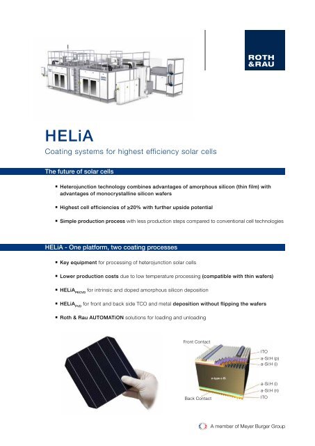
<strong>HELiA</strong><br />
Coating systems for highest efficiency solar cells<br />
The future of solar cells<br />
Heterojunction technology combines advantages of amorphous silicon (thin film) with<br />
advantages of monocrystalline silicon wafers<br />
Highest cell efficiencies of ≥20% with further upside potential<br />
Simple production process with less production steps compared to conventional cell technologies<br />
<strong>HELiA</strong> - One platform, two coating processes<br />
Key equipment for processing of heterojunction solar cells<br />
Lower production costs due to low temperature processing (compatible with thin wafers)<br />
<strong>HELiA</strong> PECVD<br />
for intrinsic and doped amorphous silicon deposition<br />
<strong>HELiA</strong> PVD<br />
for front and back side TCO and metal deposition without flipping the wafers<br />
<strong>Roth</strong> & <strong>Rau</strong> AUTOMATiON solutions for loading and unloading<br />
Front Contact<br />
ITO<br />
a-Si:H (p)<br />
a-Si:H (i)<br />
Back Contact<br />
a-Si:H (i)<br />
a-Si:H (n)<br />
ITO<br />
A member of Meyer Burger Group
Texturing<br />
PECVD 1<br />
Back Side i/n<br />
PECVD 2<br />
Front Side i/p<br />
PVD<br />
TCO Front/ Back Side<br />
Back Contact<br />
Screen<br />
Printing<br />
Curing<br />
Cell Tester<br />
& Sorter<br />
Heterojunction Technology process<br />
The Silicon heterojunction technology is an appealing<br />
concept that combines thin amorphous silicon layers with<br />
monocrystalline silicon wafers to realize cell efficiencies<br />
above 20%. The simple structure of the HJT cells needs<br />
less processing steps compared to conventional cell<br />
designs. The excellent surface passivation of the a-Si:H<br />
layer results in high cell efficiency potential.<br />
The superior temperature coefficient of T C<br />
= -0.27%/K<br />
results in a higher energy yield at operating conditions.<br />
Low temperature processing (
Texturing<br />
PECVD 1<br />
Back Side i/n<br />
PECVD 2<br />
Front Side i/p<br />
PVD<br />
TCO Front/ Back Side<br />
Back Contact<br />
Screen<br />
Printing<br />
Curing<br />
Cell Tester<br />
& Sorter<br />
Heterojunction Technology process<br />
Applications<br />
Heterojunction technology applying intrinsic, p- and n-doped a-Si:H layers using PECVD techniques. TCO and<br />
metal layers are sputtered in a PVD process.<br />
Platform<br />
The <strong>Roth</strong> & <strong>Rau</strong> <strong>HELiA</strong> platforms (PECVD and PVD) represent the key devices for processing of heterojunction<br />
solar cells. The PECVD system is capable of depositing uniform, well controlled, thin layers of intrinsic and doped<br />
a-Si:H onto a textured Si-wafer surface. The PVD system provides for front- and backside deposition without<br />
flipping the wafer. Both systems are designed for a throughput of 2400 w/h. The <strong>HELiA</strong> system platform is based<br />
on a modular design, similar to the well known SiNA ® and MAiA ® systems by <strong>Roth</strong> & <strong>Rau</strong>.<br />
<strong>HELiA</strong> PECVD<br />
- High quality a-Si:H and p/n-Si:H deposition<br />
This system is based on a modular design and,<br />
therefore, it can be configured to the specific customer<br />
needs. The layers are deposited with a PECVD process,<br />
powered by a direct RF-plasma.<br />
The high quality of the amorphous silicon layers enables<br />
the tool also for processing advanced high efficiency<br />
cells such as cells with a heterojunction rear emitter in<br />
combination with a diffused front surface field on n-type<br />
silicon. It can also be used to realize amorphous silicon<br />
backside passivated cells with a diffused emitter on<br />
p-type silicon.<br />
<strong>HELiA</strong> PVD<br />
- Large area high throughput sputtering at lowest costs<br />
This system has been developed for deposition of TCO<br />
and metal layers by sputter deposition. The tool design<br />
provides for face-up and face-down deposition – front<br />
and back side can be coated without flipping the wafer.<br />
Rotary magnetrons are used for high target utilization,<br />
good uniformity and high throughput at simultaneously<br />
low production costs. Due to its modular concept<br />
various TCO layers, metal layers and layer stacks can<br />
be deposited and make the tool applicable for the<br />
production of different solar cell concepts.<br />
Front Side<br />
Back Side
Texturing<br />
PECVD 1<br />
Back Side i/n<br />
PECVD 2<br />
Front Side i/p<br />
PVD<br />
TCO Front/ Back Side<br />
Back Contact<br />
Screen<br />
Printing<br />
Curing<br />
Cell Tester<br />
& Sorter<br />
Heterojunction Technology process<br />
<strong>HELiA</strong> PECVD<br />
- Three tool options available<br />
High level tool<br />
Medium level tool<br />
Entry level tool<br />
Cross contamination free solution<br />
Cross contamination may occur<br />
(i-, p-, n-layers)<br />
2,400 w/h throughput (both sides)<br />
optional: 4,800 w/h throughput (both sides)<br />
2,400 w/h throughput<br />
(both sides)<br />
2,400 w/h<br />
throughput<br />
(one side)<br />
Back side processing Front side processing Back side Front side Single side<br />
PM<br />
(i)<br />
PM<br />
PM<br />
(i)<br />
PM<br />
(p)<br />
PM<br />
(i)<br />
PM<br />
(i)<br />
PM<br />
(i)<br />
Cassette Loader<br />
TM<br />
TM<br />
PM<br />
(i)<br />
Handling<br />
(n)<br />
TM TM<br />
TM<br />
Flip<br />
Handling<br />
TM TM TM<br />
(n) (i)<br />
(p)<br />
PM PM PM<br />
Cassette Loader<br />
Cassette Loader<br />
TM<br />
Handling<br />
TM<br />
PM<br />
(n)<br />
Flip<br />
TM<br />
Handling<br />
TM<br />
PM<br />
(p)<br />
Cassette Loader<br />
Cassette Loader<br />
TM<br />
Handling<br />
TM<br />
PM<br />
(p)<br />
Cassette Loader<br />
Option for higher throughput<br />
<strong>HELiA</strong> PVD<br />
Waferload LM TM Transfer BM<br />
Module (In)<br />
PM<br />
(TCO)<br />
BM<br />
(Out)<br />
TM<br />
BM<br />
(In)<br />
PM<br />
(Metal)<br />
BM<br />
(Out)<br />
TM<br />
Waferload<br />
LM - Load Module<br />
TM - Transfer Module<br />
BM - Buffer Module<br />
PM - Process Module<br />
Data sheet <strong>HELiA</strong><br />
Wafer size<br />
6“ wafer<br />
Wafer type<br />
Throughput<br />
n-, or p-type mono<br />
2,400 w/h (optional: 4,800 w/h)<br />
<strong>Roth</strong> & <strong>Rau</strong> <strong>AG</strong>, info@roth-rau.com, www.roth-rau.com