Features - Bodo's Power
Features - Bodo's Power
Features - Bodo's Power
You also want an ePaper? Increase the reach of your titles
YUMPU automatically turns print PDFs into web optimized ePapers that Google loves.
age-mode or PWM technique, and can deliver up to 88% efficiency<br />
along with providing a fast transient response. Output voltage regulation<br />
is achieved by dual over-lapping modulation using both peak primary<br />
current modulation and duty-cycle modulation.<br />
The differential operation of the DCM comparator allows the LT3751<br />
to accurately operate from high-voltage inputs of up to 400V, and<br />
higher. Furthermore, the VOUT comparator and DCM comparator are<br />
needed for lower input voltages down to 4.75V, with the use of a<br />
logic-level external MOSFET. This permits the user to accommodate<br />
an extremely wide range of power sources. Only five external resistors<br />
are needed to operate the LT3751 as a capacitor charger. The<br />
output voltage trip point (VOUT) can be adjusted from 50V to 450V<br />
by using the following equation:<br />
R9 =<br />
0.98 x N______<br />
� �<br />
VOUT + VDIODES<br />
where N is the turns ratio of the transformer and VDIODES is the<br />
voltage drop across D1 and D2.<br />
The LT3751 stops charging the output capacitor once the programmed<br />
output voltage trip point is reached. The charge cycle is<br />
repeated by toggling the CHARGE pin. The maximum charge/discharge<br />
rate in the output capacitor is limited by the temperature rise<br />
in the transformer and power dissipation in the external MOSFET.<br />
Limiting the transformer surface temperature in figure 1 to 40?C rise<br />
above the ambient temperature with no air flow requires the average<br />
output power to be less than or equal to 40W, as given by:<br />
PAVE = ½ • COUT • freq • ( 2 • VOUT • VRIPPLE - V 2 RIPPLE ) � 40W<br />
Where VOUT is the output trip voltage, VRIPPLE is the output ripple<br />
voltage, and freq is the charge/discharge frequency. The maximum<br />
available output power can be increased by making the transformer<br />
larger and providing force air cooling. For output voltages higher than<br />
450V, the transformer in Figure 1 must be replaced with one having a<br />
higher turns ratio and higher primary inductance. Figure 2 shows the<br />
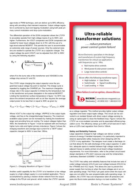
charging waveform and average input current for a 100?F output<br />
capacitor charged to 400V in less than 100ms.<br />
Figure 2 – Charging Waveform of Figure 1 Circuit<br />
X R8<br />
Another useful capability for the LT3751 is to transform a low voltage<br />
supply to a high-voltage supply in a non-isolated application. This is<br />
accomplished by placing a resistor divider network from the output<br />
voltage to the FB pin and ground, which makes the LT3751 operate<br />
POWER SUPPLY<br />
Ultra-reliable<br />
transformer solutions<br />
. . . reduce premature<br />
power control system failure!<br />
Bicron Electronics specializes in the design<br />
and manufacture of custom high frequency<br />
transformers for critical-use applications<br />
with frequencies up to 1 Mhz.<br />
Rail/marine drive controls<br />
Wind power & solar power controls<br />
Large motor drive controls<br />
High Isolation<br />
Switchmode<br />
Load Leveling<br />
Gate Drives<br />
Signal Conditioning<br />
Pulse<br />
as a voltage regulator. This method provides tighter output voltage<br />
regulation and lower output ripple voltage. This circuit can be converted<br />
to an isolated flyback with direct output voltage sensing by<br />
using an optocoupler to close the feedback loop. Figure 3 shows the<br />
LT3751 as a non-isolated converter and its associated efficiency/regulation<br />
curve. The efficiency ramps up to 88% at full load and it maintains<br />
a 0.25% load regulation from 5mA to 100mA.<br />
Safety and Reliability <strong>Features</strong><br />
Large capacitors charged to high voltages can deliver a lethal<br />
amount of energy if handled improperly. It is particularly important to<br />
observe appropriate safety measures when designing with the<br />
LT3751 in any application. The designer must create a discharge circuit<br />
that allows for the safe discharge of the output capacitor. In addition,<br />
adequate space is needed between high voltage nodes from<br />
adjacent traces to satisfy printed circuit board voltage breakdown<br />
requirements. For more information, refer to the printed circuit board<br />
design standards in IPC-2221 (www.ipc.org) and the Underwriters<br />
Laboratory Standard UL60950-1 2nd edition.<br />
The LT3751 has safety and reliability features that include two sets of<br />
under-voltage lockouts (UVLO) and over-voltage lockouts (OVLO) for<br />
the VTRANS and VCC inputs. This allows the user to prevent the<br />
power supply from turning on when the input voltages are in an unsafe<br />
operating range. The FAULT pin goes active when the input voltages<br />
are not within the user programmable safe operating range. In<br />
addition, the LT3751 has over temperature latch off protection and<br />
goes into Burst mode operation during a no load condition. The<br />
www.bodospower.com August 2009 Bodo´s <strong>Power</strong> Systems ®<br />
www.bodospower.com August 2009 Bodo´s <strong>Power</strong> Systems ®<br />
www.bodospower.com August 2009 Bodo´s <strong>Power</strong> Systems ®<br />
� �<br />
�<br />
Bicron offers the following transformer types:<br />
�<br />
�<br />
�<br />
�<br />
�<br />
�<br />
When failure is not an option, choose Bicron.<br />
BICRON<br />
Electronics<br />
www.bicron-magnetics.us<br />
+45.9858.1022 � 1.860.824.5125<br />
43


