

Probing Lead Free Solder Bumps in Final Wafer Test
Probing Lead Free Solder Bumps in Final Wafer Test
Probing Lead Free Solder Bumps in Final Wafer Test

You also want an ePaper? Increase the reach of your titles
YUMPU automatically turns print PDFs into web optimized ePapers that Google loves.
Microelectronics<br />
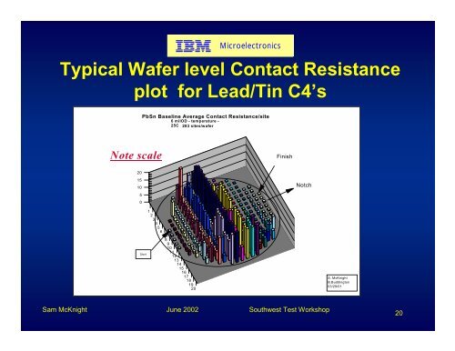
Typical <strong>Wafer</strong> level Contact Resistance<br />
plot for <strong>Lead</strong>/T<strong>in</strong> C4’s<br />
PbSn Basel<strong>in</strong>e Average Contact Resistance/site<br />
6 milOD - temperature -<br />
25C 283 sites/wafer<br />
Note scale<br />
F<strong>in</strong>ish<br />
20<br />
15<br />
10<br />
5<br />
0<br />
Notch<br />
Start<br />
1<br />
2<br />
3<br />
4<br />
5<br />
6<br />
7<br />
8<br />
9<br />
10<br />
11<br />
12<br />
13<br />
14<br />
15<br />
16<br />
17<br />
18<br />
19<br />
20<br />
S. McKnight<br />
B.Budd<strong>in</strong>gton<br />
03/29/01<br />
Sam McKnight June 2002 Southwest <strong>Test</strong> Workshop<br />
20


