

Probing Lead Free Solder Bumps in Final Wafer Test
Probing Lead Free Solder Bumps in Final Wafer Test
Probing Lead Free Solder Bumps in Final Wafer Test

You also want an ePaper? Increase the reach of your titles
YUMPU automatically turns print PDFs into web optimized ePapers that Google loves.
Microelectronics<br />
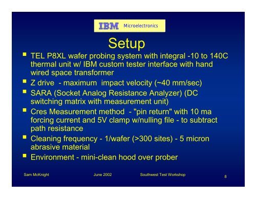
Setup<br />
TEL P8XL wafer prob<strong>in</strong>g system with <strong>in</strong>tegral -10 to 140C<br />
thermal unit w/ IBM custom tester <strong>in</strong>terface with hand<br />
wired space transformer<br />
Z drive - maximum impact velocity (~40 mm/sec)<br />
SARA (Socket Analog Resistance Analyzer) (DC<br />
switch<strong>in</strong>g matrix with measurement unit)<br />
Cres Measurement method - "p<strong>in</strong> return" with 10 ma<br />
forc<strong>in</strong>g current and 5V clamp w/null<strong>in</strong>g file - to subtract<br />
path resistance<br />
Clean<strong>in</strong>g frequency - 1/wafer (>300 sites) - 5 micron<br />
abrasive material<br />
Environment - m<strong>in</strong>i-clean hood over prober<br />
Sam McKnight June 2002 Southwest <strong>Test</strong> Workshop<br />
8


