F35-XXL Hardware description - Falcom
F35-XXL Hardware description - Falcom
F35-XXL Hardware description - Falcom

Create successful ePaper yourself
Turn your PDF publications into a flip-book with our unique Google optimized e-Paper software.
<strong>F35</strong>-<strong>XXL</strong> HARDWARE DESCRIPTION VERSION 1.10<br />
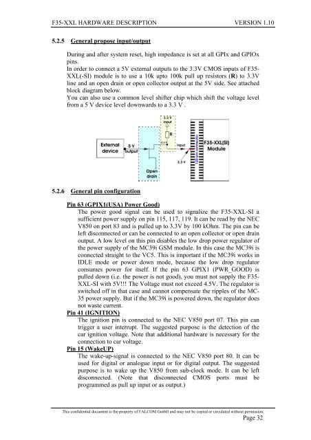
5.2.5 General propose input/output<br />
During and after system reset, high impedance is set at all GPIx and GPIOx<br />
pins.<br />
In order to connect a 5V external outputs to the 3.3V CMOS inputs of <strong>F35</strong>-<br />
<strong>XXL</strong>(-SI) module is to use a 10k upto 100k pull up resistors (R) to 3.3V<br />
line and an open drain or open collector output at the 5V side. See attached<br />
block diagram below.<br />
You can also use a common level shifter chip which shift the voltage level<br />
from a 5 V device level downwards to a 3.3 V .<br />
5.2.6 General pin configuration<br />
Pin 63 (GPIX1(USA) Power Good)<br />
The power good signal can be used to signalize the <strong>F35</strong>-<strong>XXL</strong>-SI a<br />
sufficient power supply on pin 115, 117, 119. It can be read by the NEC<br />
V850 on port 83 and is pulled up to 3.3V by 100 kOhm. The pin can be<br />
left disconnected or can be connected to an open collector or open drain<br />
output. A low level on this pin disables the low drop power regulator of<br />
the power supply of the MC39i GSM module. In this case the MC39i is<br />
connected straight to the VC5. This is important if the MC39i works in<br />
IDLE mode or power down mode, because the low drop regulator<br />
consumes power for itself. If the pin 63 GPIX1 (PWR_GOOD) is<br />
pulled down (i.e. the power is not good), you must not supply the <strong>F35</strong>-<br />
<strong>XXL</strong>-SI with 5V!!! The Voltage must not exceed 4.5V. The regulator is<br />
switched off in that case and cannot compensate the ripples of the MC-<br />
35 power supply. But if the MC39i is powered down, the regulator does<br />
not waste current.<br />
Pin 41 (IGNITION)<br />
The ignition pin is connected to the NEC V850 port 07. This pin can<br />
trigger a user interrupt. The suggested purpose is the detection of the<br />
car ignition voltage. Note that additional hardware is necessary for the<br />
connection to car voltage.<br />
Pin 15 (WakeUP)<br />
The wake-up-signal is connected to the NEC V850 port 80. It can be<br />
used for digital or analogue input or for digital output. The suggested<br />
purpose is to wake up the V850 from sub-clock mode. It can be left<br />
disconnected. (Note that disconnected CMOS ports must be<br />
programmed as pull up input or as output.)<br />
This confidential document is the property of FALCOM GmbH and may not be copied or circulated without permission.<br />
Page 32